EEL 4768 Computer Architecture Lecture 9 MultiCycle Datapath
- Slides: 37

EEL 4768 Computer Architecture Lecture 9: Multi-Cycle Datapath

Outline • Five Stages • Multi-Cycle Control • Clock Cycle Time

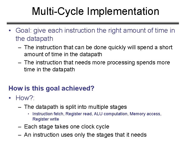
Multi-Cycle Implementation • Goal: give each instruction the right amount of time in the datapath – The instruction that can be done quickly will spend a short amount of time in the datapath – The instruction that needs more processing spends more time in the datapath How is this goal achieved? • How? : – The datapath is split into multiple stages • Instruction fetch, Register read, ALU computation, Memory access, Register write – Each stage takes one clock cycle – An instruction uses only the stages that it needs

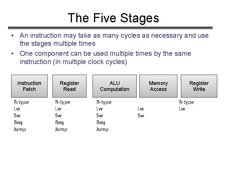
The Five Stages • An instruction may take as many cycles as necessary and use the stages multiple times • One component can be used multiple times by the same instruction (in multiple clock cycles) Instruction Fetch R-type Lw Sw Beq Jump Register Read R-type Lw Sw Beq Jump ALU Computation R-type Lw Sw Beq Jump Memory Access Lw Sw Register Write R-type Lw

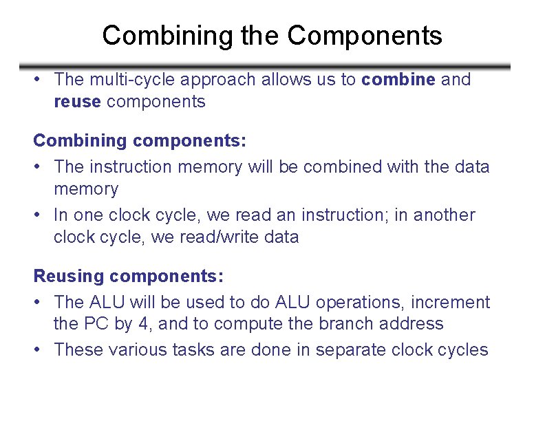
Combining the Components • The multi-cycle approach allows us to combine and reuse components Combining components: • The instruction memory will be combined with the data memory • In one clock cycle, we read an instruction; in another clock cycle, we read/write data Reusing components: • The ALU will be used to do ALU operations, increment the PC by 4, and to compute the branch address • These various tasks are done in separate clock cycles

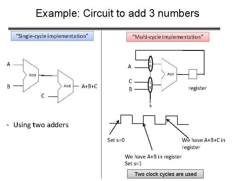
Example: Circuit to add 3 numbers “Single-cycle implementation” “Multi-cycle implementation” A A B C B A+B+C C 1 0 register s - Using two adders Set s=0 We have A+B+C in register We have A+B in register Set s=1 Two clock cycles are used

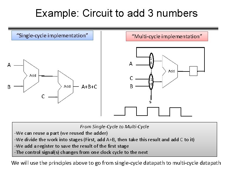
Example: Circuit to add 3 numbers “Single-cycle implementation” “Multi-cycle implementation” A A B C B A+B+C C 1 0 s From Single-Cycle to Multi-Cycle -We can reuse a part (we reused the adder) -We divide the work into stages (First, add A+B, then take this result and add C to it) -We add a register to save the result of the first stage -The control signal(s) changes from one clock cycle to the next We will use the principles above to go from single-cycle datapath to multi-cycle datapath

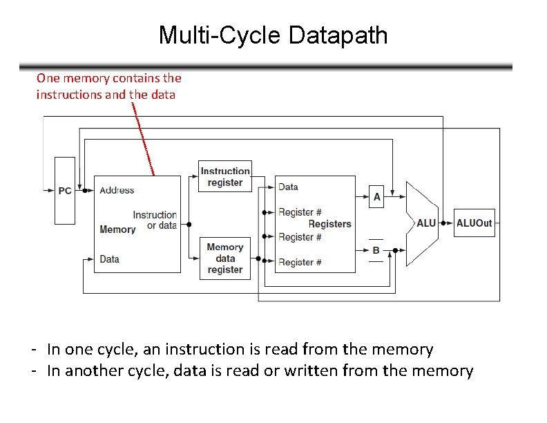
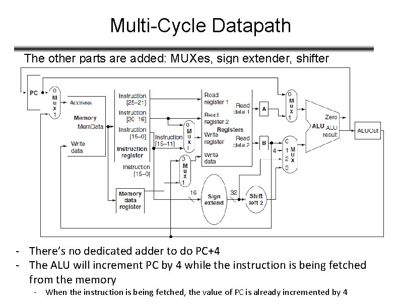
Multi-Cycle Datapath One memory contains the instructions and the data - In one cycle, an instruction is read from the memory - In another cycle, data is read or written from the memory

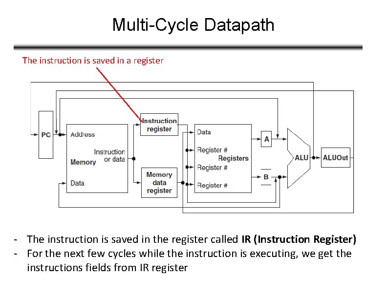
Multi-Cycle Datapath The instruction is saved in a register - The instruction is saved in the register called IR (Instruction Register) - For the next few cycles while the instruction is executing, we get the instructions fields from IR register

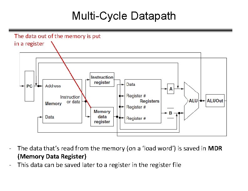
Multi-Cycle Datapath The data out of the memory is put in a register - The data that’s read from the memory (on a ‘load word’) is saved in MDR (Memory Data Register) - This data can be saved later to a register in the register file

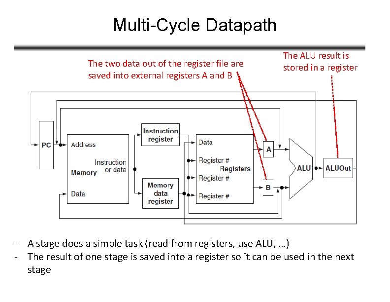
Multi-Cycle Datapath The two data out of the register file are saved into external registers A and B The ALU result is stored in a register - A stage does a simple task (read from registers, use ALU, …) - The result of one stage is saved into a register so it can be used in the next stage

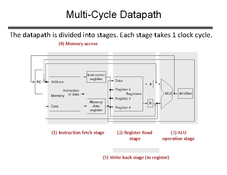
Multi-Cycle Datapath The datapath is divided into stages. Each stage takes 1 clock cycle. (4) Memory access (1) Instruction fetch stage (2) Register Read stage (3) ALU operation stage (5) Write back stage (to register)

Multi-Cycle Datapath The other parts are added: MUXes, sign extender, shifter - There’s no dedicated adder to do PC+4 - The ALU will increment PC by 4 while the instruction is being fetched from the memory - When the instruction is being fetched, the value of PC is already incremented by 4

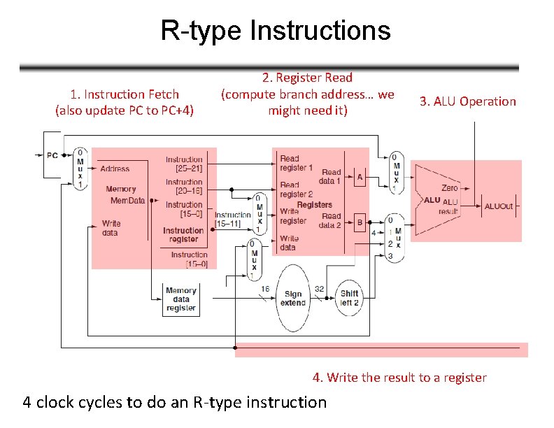
R-type Instructions 1. Instruction Fetch (also update PC to PC+4) 2. Register Read (compute branch address… we might need it) 3. ALU Operation 4. Write the result to a register 4 clock cycles to do an R-type instruction

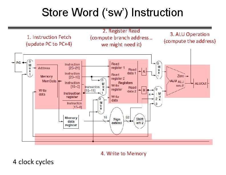
Store Word (‘sw’) Instruction 1. Instruction Fetch (update PC to PC+4) 2. Register Read (compute branch address… we might need it) 4. Write to Memory 4 clock cycles 3. ALU Operation (compute the address)

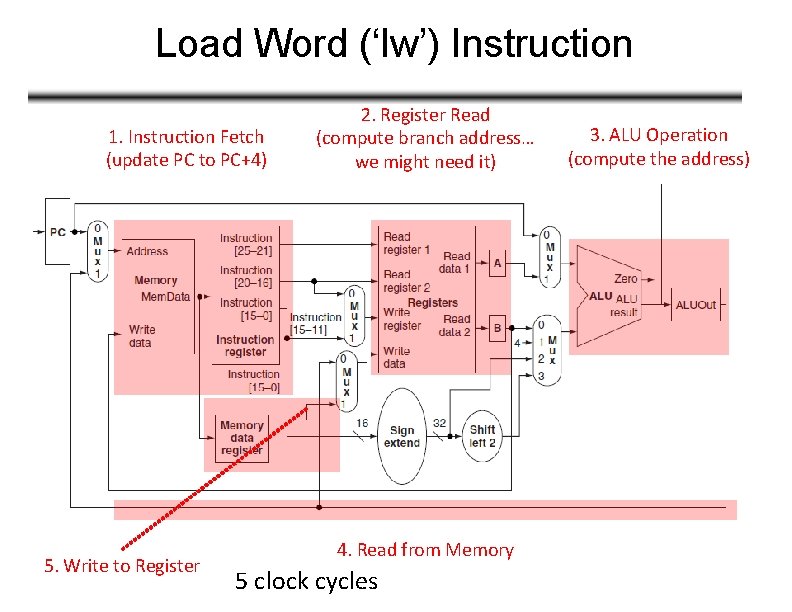
Load Word (‘lw’) Instruction 1. Instruction Fetch (update PC to PC+4) 5. Write to Register 2. Register Read (compute branch address… we might need it) 4. Read from Memory 5 clock cycles 3. ALU Operation (compute the address)

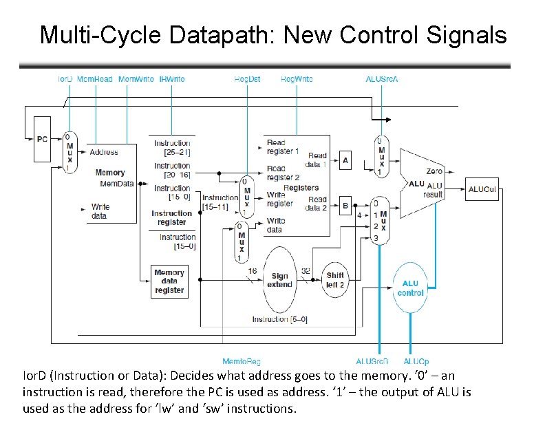
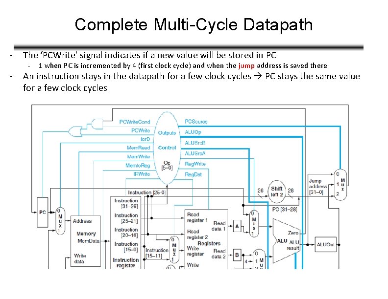
Multi-Cycle Datapath: New Control Signals Ior. D (Instruction or Data): Decides what address goes to the memory. ‘ 0’ – an instruction is read, therefore the PC is used as address. ‘ 1’ – the output of ALU is used as the address for ‘lw’ and ‘sw’ instructions.

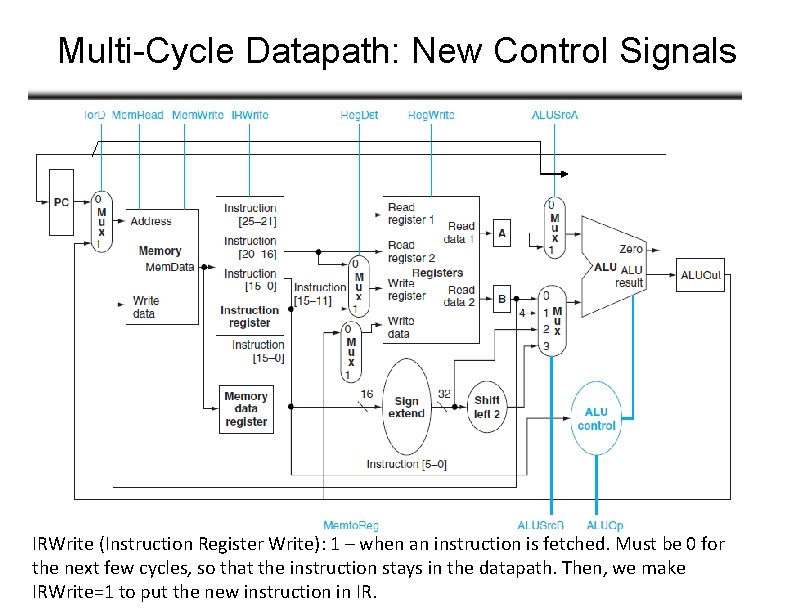
Multi-Cycle Datapath: New Control Signals IRWrite (Instruction Register Write): 1 – when an instruction is fetched. Must be 0 for the next few cycles, so that the instruction stays in the datapath. Then, we make IRWrite=1 to put the new instruction in IR.

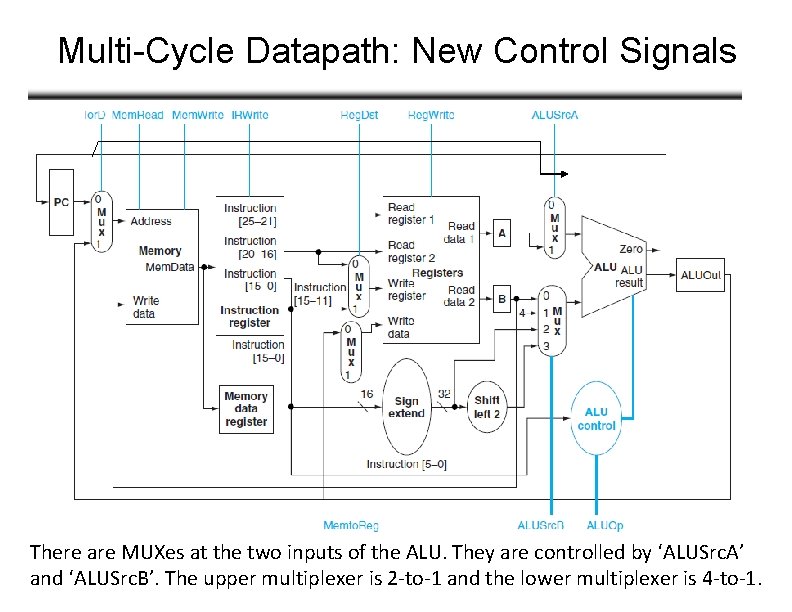
Multi-Cycle Datapath: New Control Signals There are MUXes at the two inputs of the ALU. They are controlled by ‘ALUSrc. A’ and ‘ALUSrc. B’. The upper multiplexer is 2 -to-1 and the lower multiplexer is 4 -to-1.

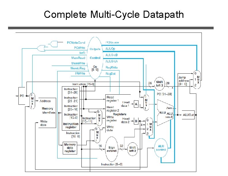
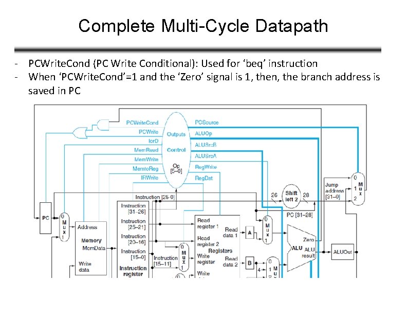
Complete Multi-Cycle Datapath

Complete Multi-Cycle Datapath - The ‘PCWrite’ signal indicates if a new value will be stored in PC - An instruction stays in the datapath for a few clock cycles PC stays the same value for a few clock cycles - 1 when PC is incremented by 4 (first clock cycle) and when the jump address is saved there

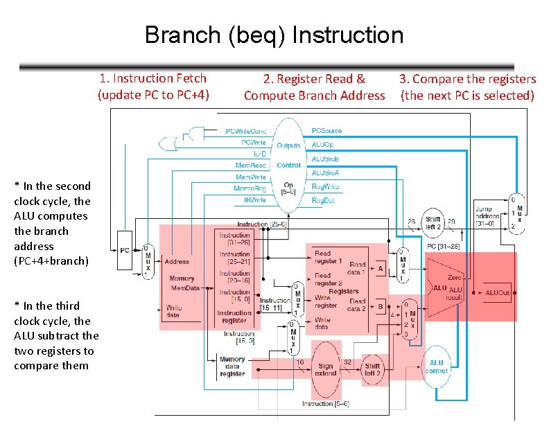
Complete Multi-Cycle Datapath - PCWrite. Cond (PC Write Conditional): Used for ‘beq’ instruction - When ‘PCWrite. Cond’=1 and the ‘Zero’ signal is 1, then, the branch address is saved in PC

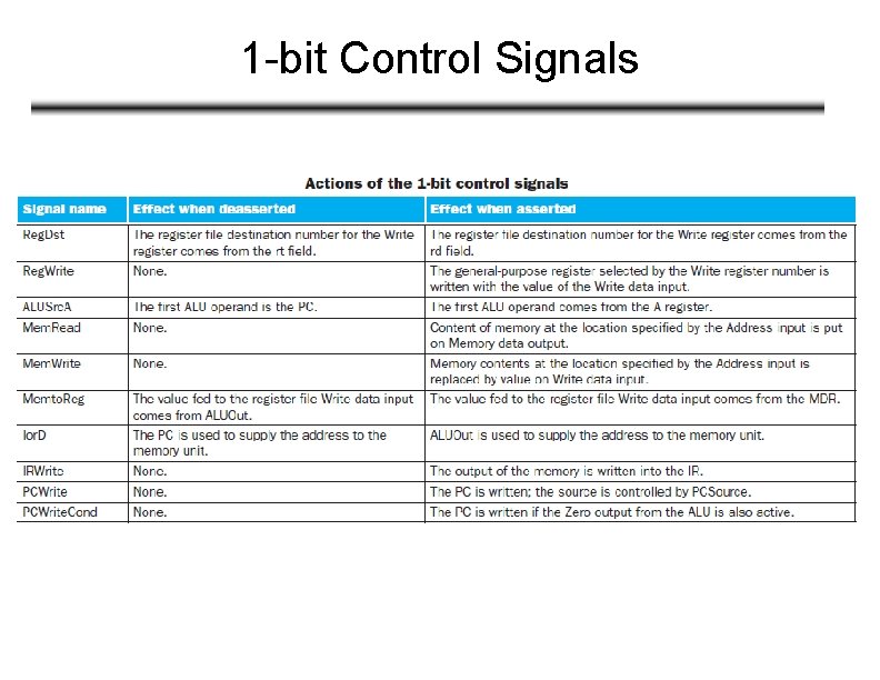
1 -bit Control Signals

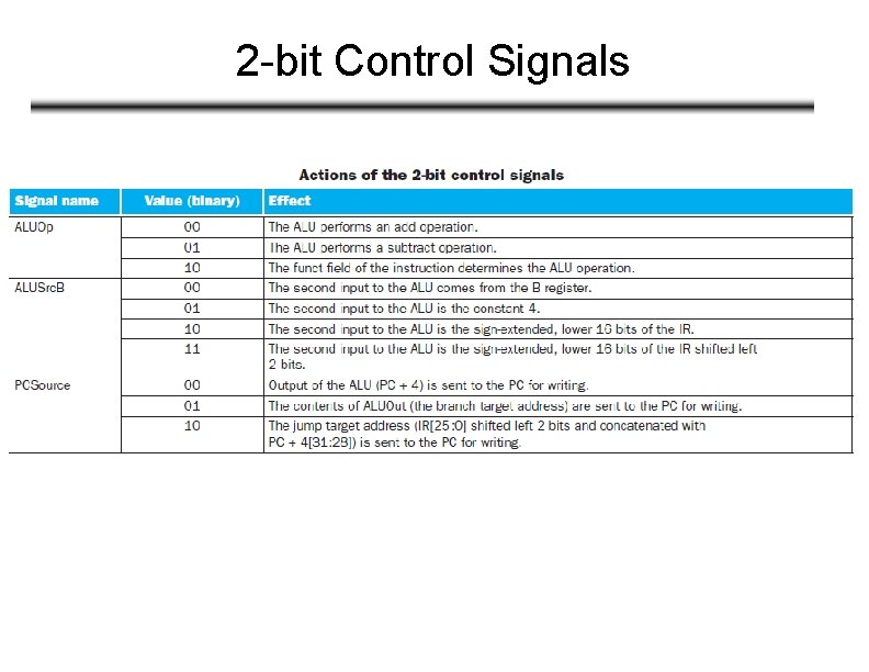
2 -bit Control Signals

Branch (beq) Instruction 1. Instruction Fetch (update PC to PC+4) * In the second clock cycle, the ALU computes the branch address (PC+4+branch) * In the third clock cycle, the ALU subtract the two registers to compare them 2. Register Read & Compute Branch Address 3. Compare the registers (the next PC is selected)

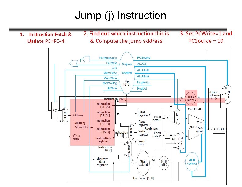
Jump (j) Instruction 1. Instruction Fetch & Update PC=PC+4 2. Find out which instruction this is & Compute the jump address 3. Set PCWrite=1 and PCSource = 10

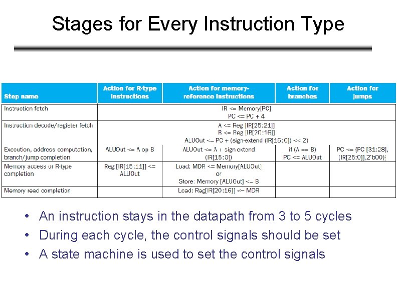
Stages for Every Instruction Type • An instruction stays in the datapath from 3 to 5 cycles • During each cycle, the control signals should be set • A state machine is used to set the control signals

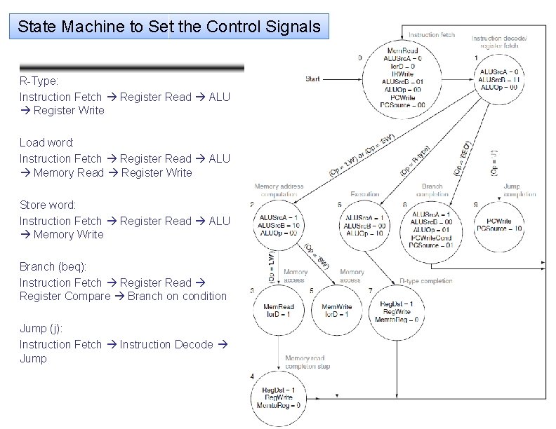
State Machine to Set the Control Signals R-Type: Instruction Fetch Register Read ALU Register Write Load word: Instruction Fetch Register Read ALU Memory Read Register Write Store word: Instruction Fetch Register Read ALU Memory Write Branch (beq): Instruction Fetch Register Read Register Compare Branch on condition Jump (j): Instruction Fetch Instruction Decode Jump

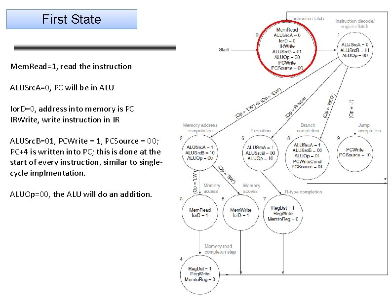
First State Mem. Read=1, read the instruction ALUSrc. A=0, PC will be in ALU Ior. D=0, address into memory is PC IRWrite, write instruction in IR ALUSrc. B=01, PCWrite = 1, PCSource = 00; PC+4 is written into PC; this is done at the start of every instruction, similar to singlecycle implmentation. ALUOp=00, the ALU will do an addition.

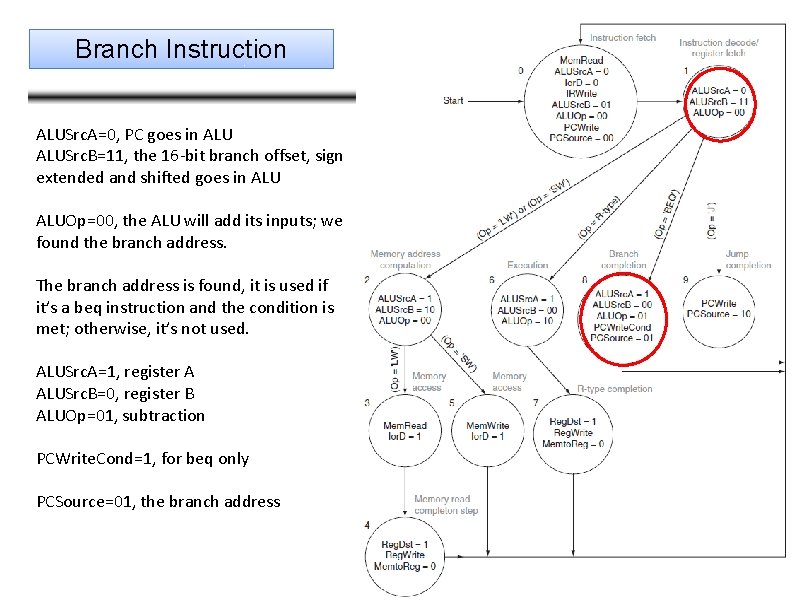
Branch Instruction ALUSrc. A=0, PC goes in ALUSrc. B=11, the 16 -bit branch offset, sign extended and shifted goes in ALUOp=00, the ALU will add its inputs; we found the branch address. The branch address is found, it is used if it’s a beq instruction and the condition is met; otherwise, it’s not used. ALUSrc. A=1, register A ALUSrc. B=0, register B ALUOp=01, subtraction PCWrite. Cond=1, for beq only PCSource=01, the branch address

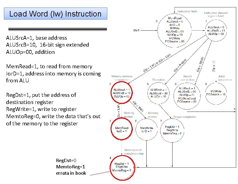
Load Word (lw) Instruction ALUSrc. A=1, base address ALUSrc. B=10, 16 -bit sign extended ALUOp=00, addition Mem. Read=1, to read from memory Ior. D=1, address into memory is coming from ALU Reg. Dst=1, put the address of destination register Reg. Write=1, write to register Memto. Reg=0, write the data that’s out of the memory to the register Reg. Dst=0 Memto. Reg=1 errata in book

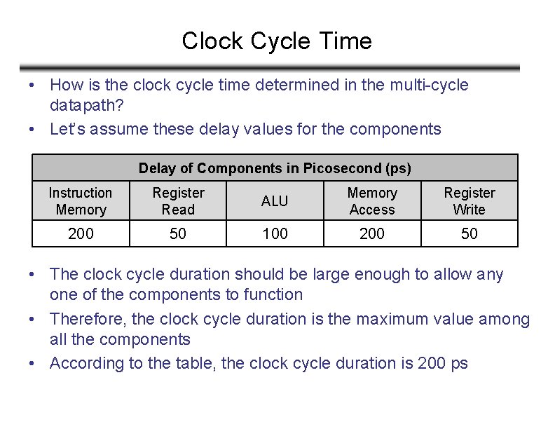
Clock Cycle Time • How is the clock cycle time determined in the multi-cycle datapath? • Let’s assume these delay values for the components Delay of Components in Picosecond (ps) Instruction Memory Register Read ALU Memory Access Register Write 200 50 100 200 50 • The clock cycle duration should be large enough to allow any one of the components to function • Therefore, the clock cycle duration is the maximum value among all the components • According to the table, the clock cycle duration is 200 ps

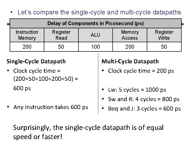
• Let’s compare the single-cycle and multi-cycle datapaths Delay of Components in Picosecond (ps) Instruction Memory Register Read ALU Memory Access Register Write 200 50 100 200 50 Single-Cycle Datapath • Clock cycle time = (200+50+100+200+50) = 600 ps • Any instruction takes 600 ps Multi-Cycle Datapath • Clock cycle time = 200 ps • Lw: 5 cycles = 1000 ps • Sw and R: 4 cycles = 800 ps • Beq and J: 3 cycles = 600 ps Surprisingly, the single-cycle datapath is of equal speed or faster!

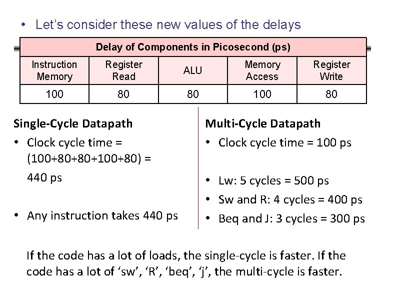
• Let’s consider these new values of the delays Delay of Components in Picosecond (ps) Instruction Memory Register Read ALU Memory Access Register Write 100 80 80 100 80 Single-Cycle Datapath • Clock cycle time = (100+80+80+100+80) = 440 ps • Any instruction takes 440 ps Multi-Cycle Datapath • Clock cycle time = 100 ps • Lw: 5 cycles = 500 ps • Sw and R: 4 cycles = 400 ps • Beq and J: 3 cycles = 300 ps If the code has a lot of loads, the single-cycle is faster. If the code has a lot of ‘sw’, ‘R’, ‘beq’, ‘j’, the multi-cycle is faster.

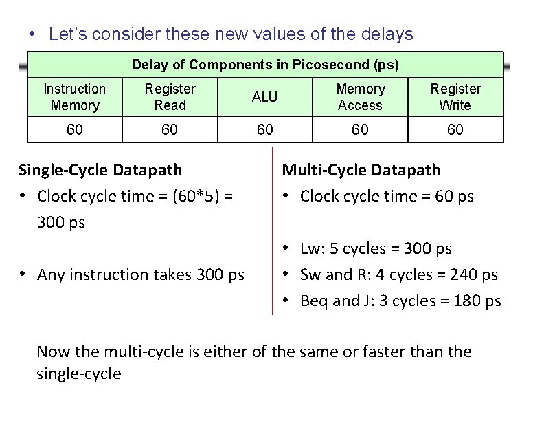
• Let’s consider these new values of the delays Delay of Components in Picosecond (ps) Instruction Memory Register Read ALU Memory Access Register Write 60 60 60 Single-Cycle Datapath • Clock cycle time = (60*5) = 300 ps • Any instruction takes 300 ps Multi-Cycle Datapath • Clock cycle time = 60 ps • Lw: 5 cycles = 300 ps • Sw and R: 4 cycles = 240 ps • Beq and J: 3 cycles = 180 ps Now the multi-cycle is either of the same or faster than the single-cycle

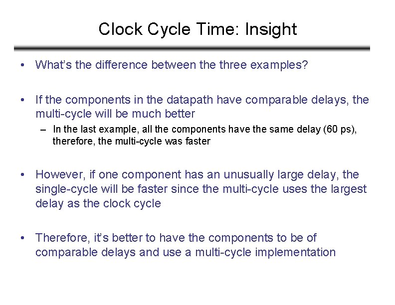
Clock Cycle Time: Insight • What’s the difference between the three examples? • If the components in the datapath have comparable delays, the multi-cycle will be much better – In the last example, all the components have the same delay (60 ps), therefore, the multi-cycle was faster • However, if one component has an unusually large delay, the single-cycle will be faster since the multi-cycle uses the largest delay as the clock cycle • Therefore, it’s better to have the components to be of comparable delays and use a multi-cycle implementation

Readings • H&P COD – Chapter 4