EEL 4744 Microprocessor Applications Serial Communication Interface Presented

- Slides: 28

EEL 4744 Microprocessor Applications Serial Communication Interface Presented by: Damian Szmulewicz University of Florida

Sources • TI SPRS 439 F: Data Manual • TI SPRUFZ 5 A: 2823 x Serial Communications Interface (SCI) Reference Guide. – Pages: 12 -16, 21 -22, 26 -35 • TI SPRUB 0 C: System Control and Interrupt Reference Guide. – Pages: 122, 123, 139 -142

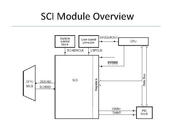
SCI Module Overview

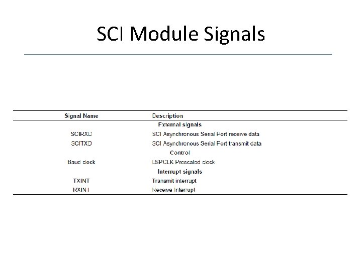
SCI Module Signals

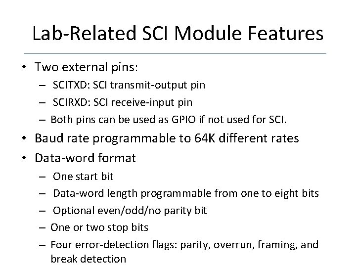
Lab-Related SCI Module Features • Two external pins: – SCITXD: SCI transmit-output pin – SCIRXD: SCI receive-input pin – Both pins can be used as GPIO if not used for SCI. • Baud rate programmable to 64 K different rates • Data-word format – – – One start bit Data-word length programmable from one to eight bits Optional even/odd/no parity bit One or two stop bits Four error-detection flags: parity, overrun, framing, and break detection

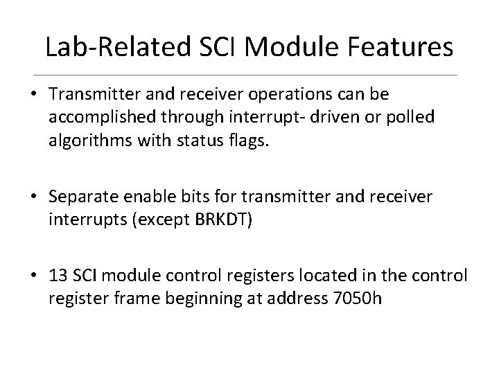
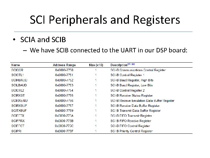
Lab-Related SCI Module Features • Transmitter and receiver operations can be accomplished through interrupt- driven or polled algorithms with status flags. • Separate enable bits for transmitter and receiver interrupts (except BRKDT) • 13 SCI module control registers located in the control register frame beginning at address 7050 h

SCI Peripherals and Registers • SCIA and SCIB – We have SCIB connected to the UART in our DSP board:

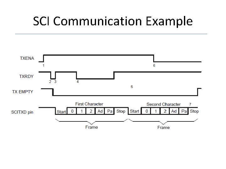
SCI Communication Example

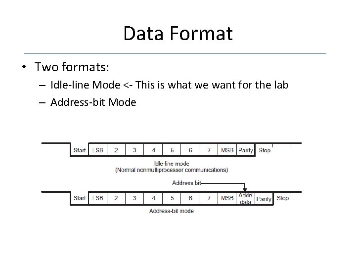
Data Format • Two formats: – Idle-line Mode <- This is what we want for the lab – Address-bit Mode

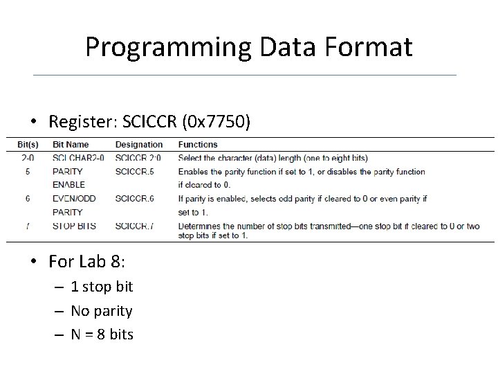
Programming Data Format • Register: SCICCR (0 x 7750) • For Lab 8: – 1 stop bit – No parity – N = 8 bits

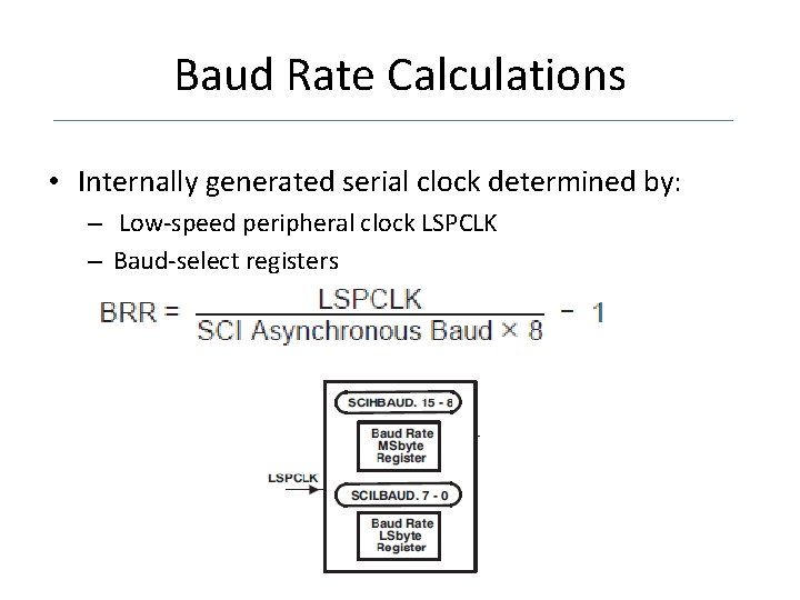
Baud Rate Calculations • Internally generated serial clock determined by: – Low-speed peripheral clock LSPCLK – Baud-select registers

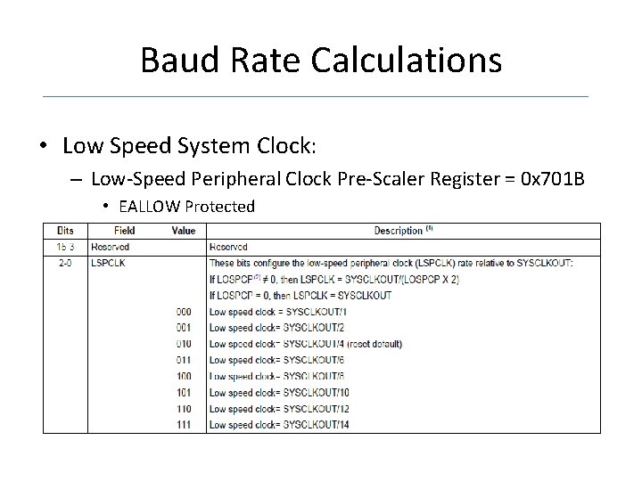
Baud Rate Calculations • Low Speed System Clock: – Low-Speed Peripheral Clock Pre-Scaler Register = 0 x 701 B • EALLOW Protected

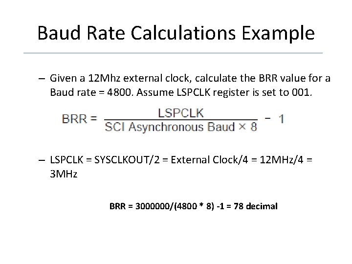
Baud Rate Calculations Example – Given a 12 Mhz external clock, calculate the BRR value for a Baud rate = 4800. Assume LSPCLK register is set to 001. – LSPCLK = SYSCLKOUT/2 = External Clock/4 = 12 MHz/4 = 3 MHz BRR = 3000000/(4800 * 8) -1 = 78 decimal

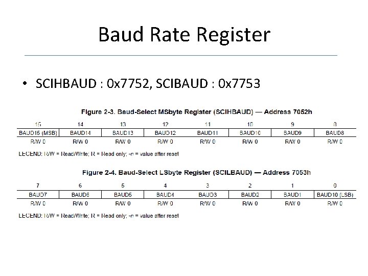
Baud Rate Register • SCIHBAUD : 0 x 7752, SCIBAUD : 0 x 7753

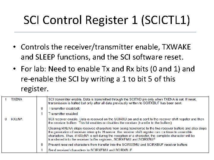
SCI Control Register 1 (SCICTL 1) • Controls the receiver/transmitter enable, TXWAKE and SLEEP functions, and the SCI software reset. • For lab: Need to enable Tx and Rx bits (0 and 1) and re-enable the SCI by writing a 1 to bit 5 of this register.

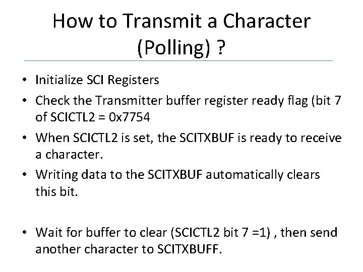
How to Transmit a Character (Polling) ? • Initialize SCI Registers • Check the Transmitter buffer register ready flag (bit 7 of SCICTL 2 = 0 x 7754 • When SCICTL 2 is set, the SCITXBUF is ready to receive a character. • Writing data to the SCITXBUF automatically clears this bit. • Wait for buffer to clear (SCICTL 2 bit 7 =1) , then send another character to SCITXBUFF.

SCI Interrupt Controlled • The SCICTL 2 register has one flag bit (TXRDY) that indicates active interrupt conditions, and the SCIRXST register has two interrupt flag bits (RXRDY and BRKDT) • The transmitter and receiver have separate interrupt -enable bits

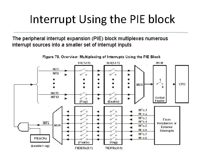
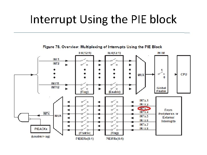
Interrupt Using the PIE block The peripheral interrupt expansion (PIE) block multiplexes numerous interrupt sources into a smaller set of interrupt inputs

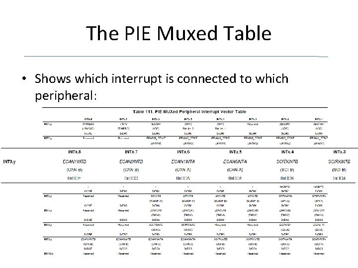
The PIE Muxed Table • Shows which interrupt is connected to which peripheral:

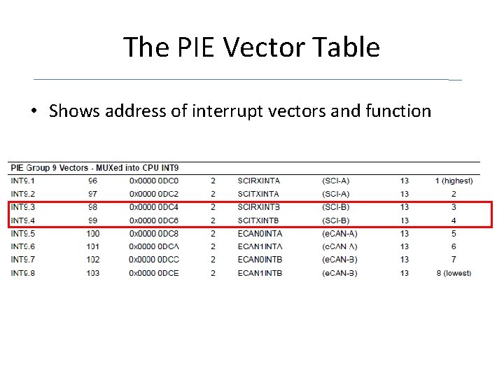
The PIE Vector Table • Shows address of interrupt vectors and function

Interrupt Using the PIE block

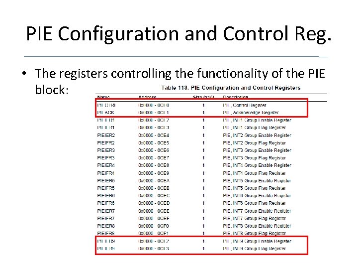
PIE Configuration and Control Reg. • The registers controlling the functionality of the PIE block:

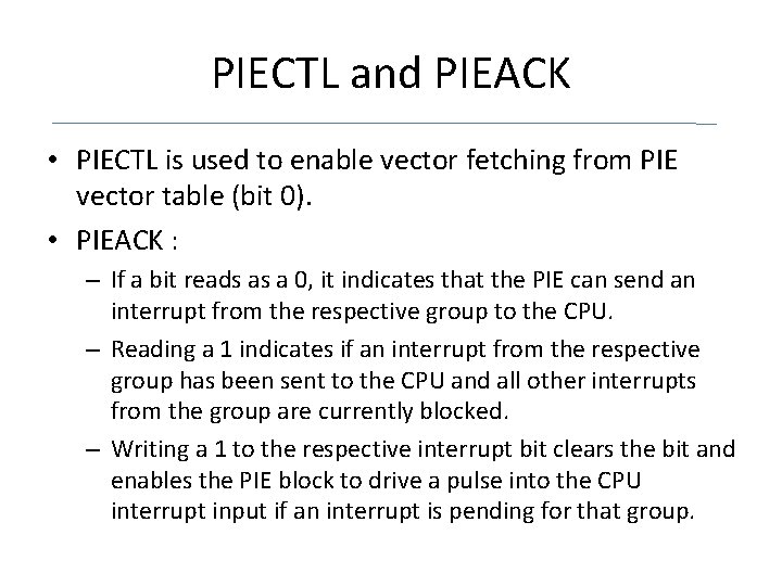
PIECTL and PIEACK • PIECTL is used to enable vector fetching from PIE vector table (bit 0). • PIEACK : – If a bit reads as a 0, it indicates that the PIE can send an interrupt from the respective group to the CPU. – Reading a 1 indicates if an interrupt from the respective group has been sent to the CPU and all other interrupts from the group are currently blocked. – Writing a 1 to the respective interrupt bit clears the bit and enables the PIE block to drive a pulse into the CPU interrupt input if an interrupt is pending for that group.

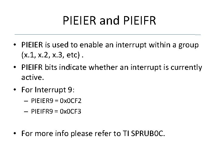
PIEIER and PIEIFR • PIEIER is used to enable an interrupt within a group (x. 1, x. 2, x. 3, etc). • PIEIFR bits indicate whether an interrupt is currently active. • For Interrupt 9: – PIEIER 9 = 0 x 0 CF 2 – PIEIFR 9 = 0 x 0 CF 3 • For more info please refer to TI SPRUB 0 C.

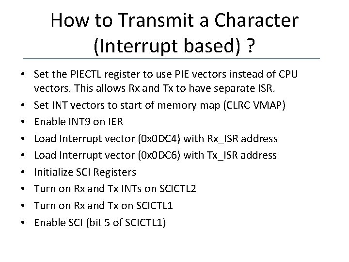
How to Transmit a Character (Interrupt based) ? • Set the PIECTL register to use PIE vectors instead of CPU vectors. This allows Rx and Tx to have separate ISR. • Set INT vectors to start of memory map (CLRC VMAP) • Enable INT 9 on IER • Load Interrupt vector (0 x 0 DC 4) with Rx_ISR address • Load Interrupt vector (0 x 0 DC 6) with Tx_ISR address • Initialize SCI Registers • Turn on Rx and Tx INTs on SCICTL 2 • Turn on Rx and Tx on SCICTL 1 • Enable SCI (bit 5 of SCICTL 1)

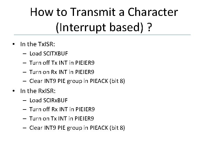
How to Transmit a Character (Interrupt based) ? • In the Tx. ISR: – – Load SCITXBUF Turn off Tx INT in PIEIER 9 Turn on Rx INT in PIEIER 9 Clear INT 9 PIE group in PIEACK (bit 8) • In the Rx. ISR: – – Load SCIRx. BUF Turn off Rx INT in PIEIER 9 Turn on Tx INT in PIEIER 9 Clear INT 9 PIE group in PIEACK (bit 8)

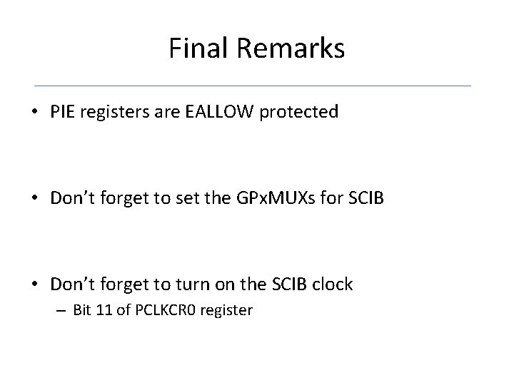
Final Remarks • PIE registers are EALLOW protected • Don’t forget to set the GPx. MUXs for SCIB • Don’t forget to turn on the SCIB clock – Bit 11 of PCLKCR 0 register

Questions? ? ?