EEE 4084 F Digital Systems Lecture 21 More




- Slides: 39

EEE 4084 F Digital Systems Lecture 21 More Verilog. Configuration Architectures. RC Building Blocks (IP Cores), basic handshaking, latches and other interface ingredients Lecturer: Simon Winberg Attribution-Share. Alike 4. 0 International (CC BY-SA 4. 0)

Lecture Overview to use assign Blocking & non-blocking simulation and potential pitfalls The unconditional always Configuration architectures Digital signals, Interface basics, Using latches When

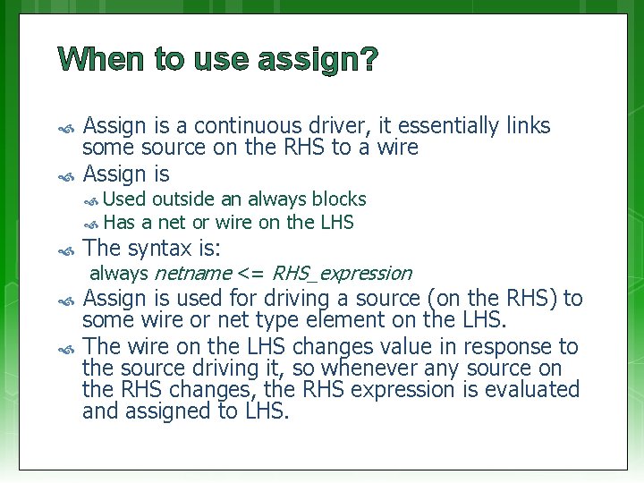
When to use assign? Assign is a continuous driver, it essentially links some source on the RHS to a wire Assign is Used outside an always blocks Has a net or wire on the LHS The syntax is: Assign is used for driving a source (on the RHS) to some wire or net type element on the LHS. The wire on the LHS changes value in response to the source driving it, so whenever any source on the RHS changes, the RHS expression is evaluated and assigned to LHS. always netname <= RHS_expression

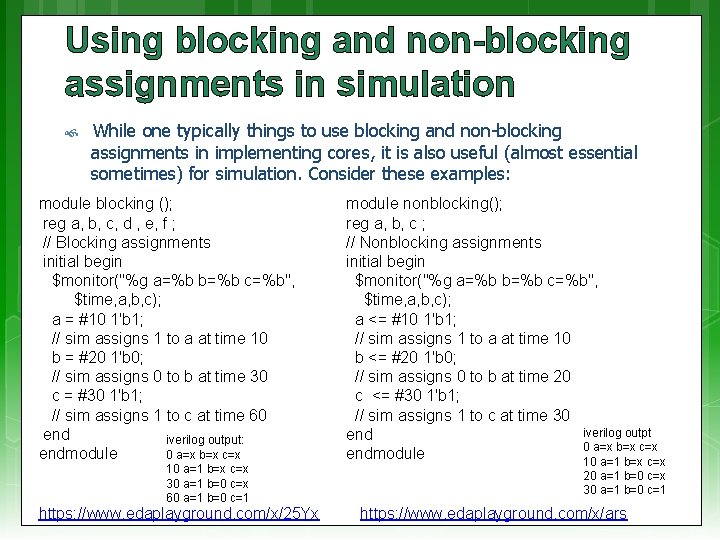
Using blocking and non-blocking assignments in simulation While one typically things to use blocking and non-blocking assignments in implementing cores, it is also useful (almost essential sometimes) for simulation. Consider these examples: module blocking (); reg a, b, c, d , e, f ; // Blocking assignments initial begin $monitor("%g a=%b b=%b c=%b", $time, a, b, c); a = #10 1'b 1; // sim assigns 1 to a at time 10 b = #20 1'b 0; // sim assigns 0 to b at time 30 c = #30 1'b 1; // sim assigns 1 to c at time 60 end iverilog output: 0 a=x b=x c=x endmodule 10 a=1 b=x c=x 30 a=1 b=0 c=x 60 a=1 b=0 c=1 https: //www. edaplayground. com/x/25 Yx module nonblocking(); reg a, b, c ; // Nonblocking assignments initial begin $monitor("%g a=%b b=%b c=%b", $time, a, b, c); a <= #10 1'b 1; // sim assigns 1 to a at time 10 b <= #20 1'b 0; // sim assigns 0 to b at time 20 c <= #30 1'b 1; // sim assigns 1 to c at time 30 iverilog outpt end 0 a=x b=x c=x endmodule 10 a=1 b=x c=x 20 a=1 b=0 c=x 30 a=1 b=0 c=1 https: //www. edaplayground. com/x/ars

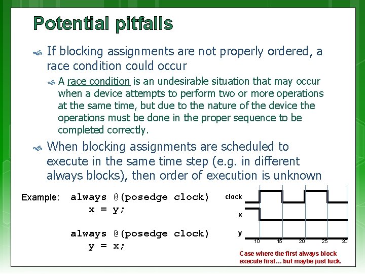
Potential pitfalls If blocking assignments are not properly ordered, a race condition could occur A race condition is an undesirable situation that may occur when a device attempts to perform two or more operations at the same time, but due to the nature of the device the operations must be done in the proper sequence to be completed correctly. When blocking assignments are scheduled to execute in the same time step (e. g. in different always blocks), then order of execution is unknown Example: always @(posedge clock) x = y; clock always @(posedge clock) y = x; y x 10 15 20 25 Case where the first always block execute first… but maybe just luck. 30

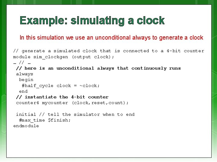
The unconditional always The always block does not necessarily need to have a sensitivity list. In such a case the always block is activated continuously This is commonly used for simulation, e. g. to generate a clock… let’s see a quick example

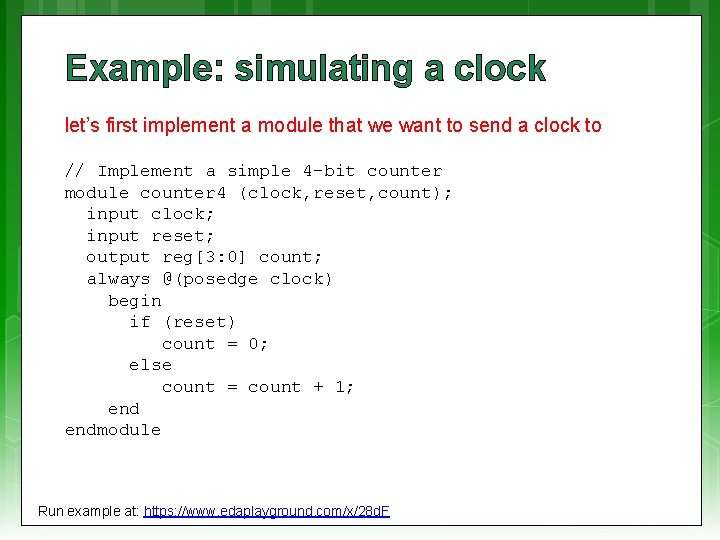
Example: simulating a clock let’s first implement a module that we want to send a clock to // Implement a simple 4 -bit counter module counter 4 (clock, reset, count); input clock; input reset; output reg[3: 0] count; always @(posedge clock) begin if (reset) count = 0; else count = count + 1; endmodule Run example at: https: //www. edaplayground. com/x/28 d. F

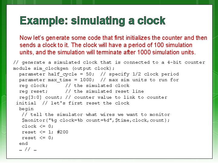
Example: simulating a clock Now let’s generate some code that first initializes the counter and then sends a clock to it. The clock will have a period of 100 simulation units, and the simulation will terminate after 1000 simulation units. // generate a simulated clock that is connected to a 4 -bit counter module sim_clockgen (output clock); parameter half_cycle = 50; // specify 1/2 clock period parameter max_time = 1000; // max sim units to run for reg clock; // the simulated clock reg reset; // the simulated reset line reg[3: 0] count; // counter value to link to counter initial // let's first reset the clock begin // tell the simulator what wires we want to monitor $monitor("%g clock=%b count=%d", $time, clock, count); clock <= 0; reset <= 1; #200 reset <= 0; end … // …

Example: simulating a clock In this simulation we use an unconditional always to generate a clock // generate a simulated clock that is connected to a 4 -bit counter module sim_clockgen (output clock); … // here is an unconditional always that continuously runs always begin #half_cycle clock = ~clock; end // instantiate the 4 -bit counter 4 mycounter (clock, reset, count); initial // tell the simulator when to end #max_time $finish; endmodule

Configuration Architectures RC Architecture

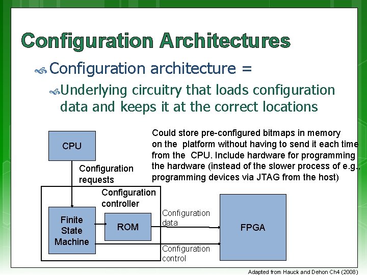
Configuration Architectures Configuration architecture = Underlying circuitry that loads configuration data and keeps it at the correct locations Could store pre-configured bitmaps in memory on the platform without having to send it each time from the CPU. Include hardware for programming the hardware (instead of the slower process of e. g. , programming devices via JTAG from the host) CPU Configuration requests Configuration controller Finite State Machine ROM Configuration data FPGA Configuration control Adapted from Hauck and Dehon Ch 4 (2008)

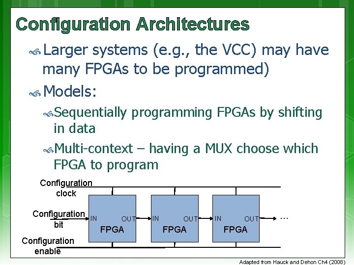
Configuration Architectures Larger systems (e. g. , the VCC) may have many FPGAs to be programmed) Models: Sequentially programming FPGAs by shifting in data Multi-context – having a MUX choose which FPGA to program Configuration clock Configuration bit IN OUT FPGA IN OUT … FPGA Configuration enable Adapted from Hauck and Dehon Ch 4 (2008)

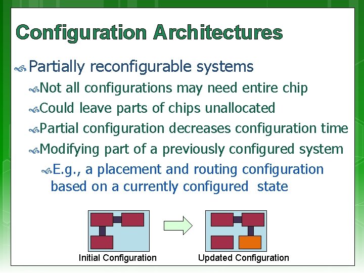
Configuration Architectures Partially reconfigurable systems Not all configurations may need entire chip Could leave parts of chips unallocated Partial configuration decreases configuration time Modifying part of a previously configured system E. g. , a placement and routing configuration based on a currently configured state Initial Configuration Updated Configuration

Configuration Architectures Block configurable architecture Not the same as “logical blocks” in an FPGA Relocating configurations to different blocks at run time also referred to as “swappable logic units” (SLUs) Example: SCORE* relocatable architecture in which configurable blocks are handled in the same way as a virtual memory system * Capsi & De. Hon and Wawrzynek. “A streaming multithreaded model” In Third workshop on media and stream processors. 2001

Additional Reading Hauck, Scott (1998). “The Roles of FPGAs in Reprogrammable Systems” In Proceedings of the IEEE. 86(4) pp. 615 -639.

RC Building Blocks: Digital Signals and Data Transfers Reconfigurable Computing Developing reusable gateware components / IP Cores

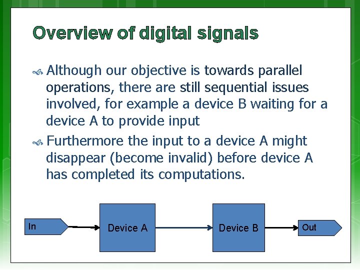
Overview of digital signals Although our objective is towards parallel operations, there are still sequential issues involved, for example a device B waiting for a device A to provide input Furthermore the input to a device A might disappear (become invalid) before device A has completed its computations. In Device A Device B Out

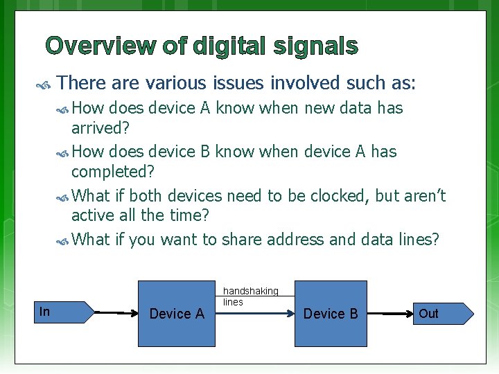
Overview of digital signals There are various issues involved such as: How does device A know when new data has arrived? How does device B know when device A has completed? What if both devices need to be clocked, but aren’t active all the time? What if you want to share address and data lines? In Device A handshaking lines Device B Out

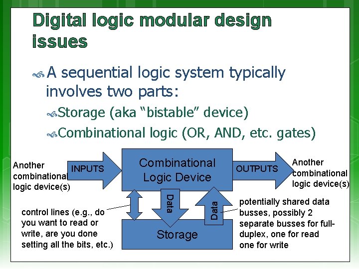
Digital logic modular design issues A sequential logic system typically involves two parts: Storage (aka “bistable” device) Combinational logic (OR, AND, etc. gates) Data control lines (e. g. , do you want to read or write, are you done setting all the bits, etc. ) Combinational Logic Device Storage Data Another INPUTS combinational logic device(s) OUTPUTS Another combinational logic device(s) potentially shared data busses, possibly 2 separate busses for fullduplex, one for read one for write

Handshaking – making sure the data gets there Reconfigurable Computing

Interface Handshaking basics Handshaking is a means to ensure reliable transfer of data and/or control between two devices that could be far apart (long latencies between pins) or could be operating at different clock frequencies. Essentially, handshaking provides additional pins to synchronize the transfer of data, so that data is sent when the receiver is ready.

Handshaking For effective data exchange: Sender needs to first know when receiver is able to receive data, and when the data has been successfully received. Receiver needs to know when the data is ready to be sent to it, and when the sender has determined that the receiver has acquired the data.

Handshaking There are many types of handshaking, but they are generally either: Explicit handshaking Implicit handshaking Information based on Digilent training resources available at: https: //reference. digilentinc. com/learn/courses/unit-3/start

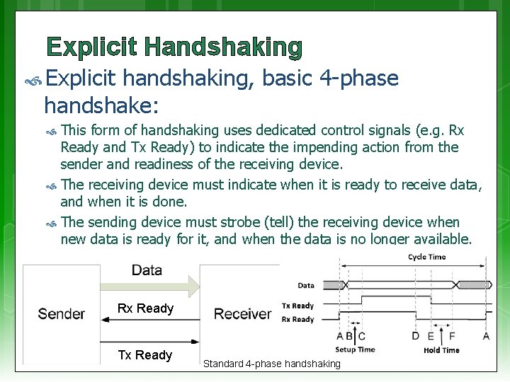
Explicit Handshaking Explicit handshaking, basic 4 -phase handshake: This form of handshaking uses dedicated control signals (e. g. Rx Ready and Tx Ready) to indicate the impending action from the sender and readiness of the receiving device. The receiving device must indicate when it is ready to receive data, and when it is done. The sending device must strobe (tell) the receiving device when new data is ready for it, and when the data is no longer available. Rx Ready Tx Ready Standard 4 -phase handshaking

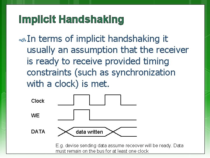
Implicit Handshaking In terms of implicit handshaking it usually an assumption that the receiver is ready to receive provided timing constraints (such as synchronization with a clock) is met. Clock WE DATA data written E. g. devise sending data assume receover will be ready. Data must remain on the bus for at least one clock

Digital Signal Interfaces Generally Address need the following bus Data bus Control lines Chip / Device select lines (CS) Write enable lines (WE) Read enable lines (RE)

Interface / Handshaking Standards Next lecture we look at a selection of interfacing standards for developing your own reusable IP cores. We also look at standard memory interfaces and DMA transfers For now though we continue on with some latching and signal capture which are essential ingredients in reliable gateware interfaces

RC Building Blocks: Latching (capturing Signals) Reconfigurable Computing

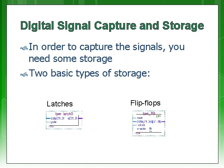
Digital Signal Capture and Storage In order to capture the signals, you need some storage Two basic types of storage: Latches Flip-flops

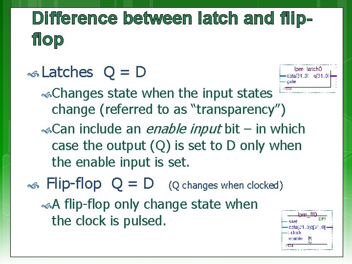
Difference between latch and flipflop Latches Q=D Changes state when the input states change (referred to as “transparency”) Can include an enable input bit – in which case the output (Q) is set to D only when the enable input is set. Flip-flop Q = D A (Q changes when clocked) flip-flop only change state when the clock is pulsed.

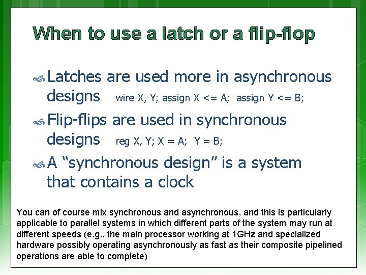
When to use a latch or a flip-flop Latches are used more in asynchronous designs wire X, Y; assign X <= A; assign Y <= B; Flip-flips are used in synchronous designs reg X, Y; X = A; Y = B; A “synchronous design” is a system that contains a clock You can of course mix synchronous and asynchronous, and this is particularly applicable to parallel systems in which different parts of the system may run at different speeds (e. g. , the main processor working at 1 GHz and specialized hardware possibly operating asynchronously as fast as their composite pipelined operations are able to complete)

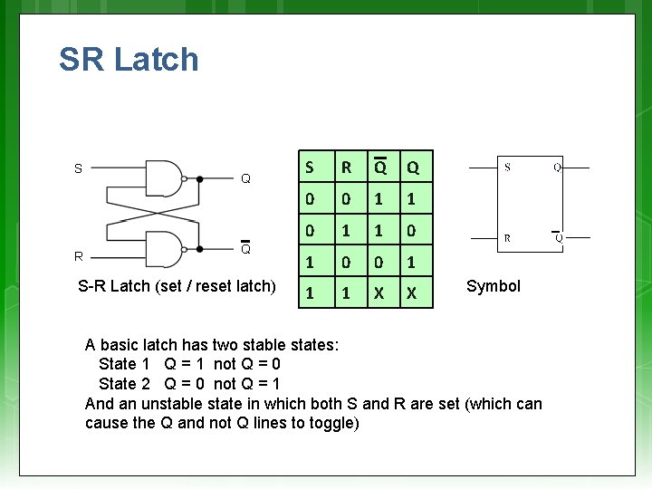
SR Latch S R Q Q S-R Latch (set / reset latch) S R Q Q 0 0 1 1 0 1 0 0 1 1 1 X X Symbol A basic latch has two stable states: State 1 Q = 1 not Q = 0 State 2 Q = 0 not Q = 1 And an unstable state in which both S and R are set (which can cause the Q and not Q lines to toggle)

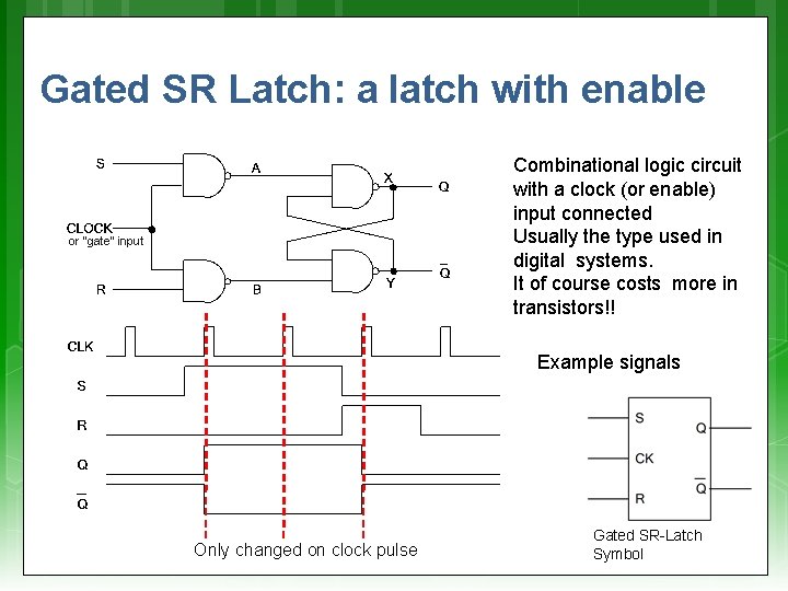
Gated SR Latch: a latch with enable Combinational logic circuit with a clock (or enable) input connected Usually the type used in digital systems. It of course costs more in transistors!! or “gate” input Example signals Only changed on clock pulse Gated SR-Latch Symbol

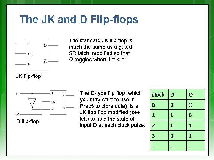
The JK and D Flip-flops The standard JK flip-flop is much the same as a gated SR latch, modified so that Q toggles when J = K = 1 JK flip-flop D flip-flop The D-type flip flop (which you may want to use in Prac 5 to store data) is a JK flop modified (see left) to hold the state of input D at each clock pulse. clock D Q 0 0 X 1 1 0 2 1 1 3 0 1 … … …

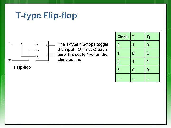
T-type Flip-flop The T-type flip-flops toggle the input. Q = not Q each time T is set to 1 when the clock pulses T flip-flop Clock T Q 0 1 0 1 2 1 1 3 0 0 … … …

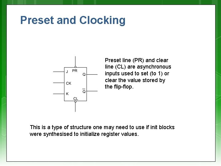
Preset and Clocking Preset line (PR) and clear line (CL) are asynchronous inputs used to set (to 1) or clear the value stored by the flip-flop. This is a type of structure one may need to use if init blocks were synthesised to initialize register values.

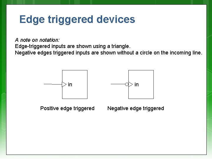
Edge triggered devices A note on notation: Edge-triggered inputs are shown using a triangle. Negative edges triggered inputs are shown without a circle on the incoming line. in Positive edge triggered in Negative edge triggered

End of Lecture Any Question? ?

Disclaimers and copyright/licensing details I have tried to follow the correct practices concerning copyright and licensing of material, particularly image sources that have been used in this presentation. I have put much effort into trying to make this material open access so that it can be of benefit to others in their teaching and learning practice. Any mistakes or omissions with regards to these issues I will correct when notified. To the best of my understanding the material in these slides can be shared according to the Creative Commons “Attribution-Share. Alike 4. 0 International (CC BY-SA 4. 0)” license, and that is why I selected that license to apply to this presentation (it’s not because I particularly want my slides referenced but more to acknowledge the sources and generosity of others who have provided free material such as the images I have used). Image sources: man working on laptop – flickr scroll, video reel, big question mark – Pixabay http: //pixabay. com/ (public domain) some diagrammatic elements are from Xilinx ISE screenshots References: Verilog code adapted from http: //www. asic-world. com/examples/verilog