EEE 132 Electronic Devices Prof Syed Idris Syed
- Slides: 57

EEE 132 Electronic Devices Prof Syed Idris Syed Hassan Mr Arjuna Marzuki Mrs Norlaili Mohd Noh

Course outcome 1 st topic o o o To understand the semiconductor materials that are suitable for electronic devices To study the properties of materials for electronic devices To understand the biasing of diode Able to design Diode circuit Able to apply some types of diodes

Assessments/Books o o o 3 Tests 15% Assignment/Tutorials 15% Examination 70% Text books: Electronic devices and circuit theory by Robert L. Boylestad and Louis Nashelsky

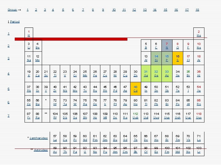
Semiconductor Material o o Semiconductors are a special class of elements having a conductivity between that of a good conductor and that of an insulator. They are fall into two classes : single crystal and compound Single crystal e. g Ge and Si Compound e. g Ga. As , Cd. S, Ga. N and Ga. As. P Ge-germanium; Si-silicon; Ga-gallium ; As –arsenide; Cd-cadmium; Ssulfide; N-nitride; P-phosphide

Group → 1 2 3 4 5 6 7 8 9 10 11 12 13 14 15 16 17 18 ↓ Period 1 1 H 2 He 2 3 Li 4 Be 5 B 6 C 7 N 8 O 9 F 10 Ne 3 11 Na 12 Mg 13 Al 14 Si 15 P 16 S 17 Cl 18 Ar 4 19 K 20 Ca 21 Sc 22 Ti 23 V 24 Cr 25 Mn 26 Fe 27 Co 28 Ni 29 Cu 30 Zn 31 Ga 32 Ge 33 As 34 Se 35 Br 36 Kr 5 37 Rb 38 Sr 39 Y 40 Zr 41 Nb 42 Mo 43 Tc 44 Ru 45 Rh 46 Pd 47 Ag 48 Cd 49 In 50 Sn 51 Sb 52 Te 53 I 54 Xe 6 55 Cs 56 Ba * 72 Hf 73 Ta 74 W 75 Re 76 Os 77 Ir 78 Pt 79 Au 80 Hg 81 Tl 82 Pb 83 Bi 84 Po 85 At 86 Rn 7 87 Fr 88 Ra ** 104 Rf 105 Db 106 Sg 107 Bh 108 Hs 109 Mt 110 Ds 111 Rg 112 Uub 113 Uut 114 Uuq 115 Uup 116 Uuh 117 Uus 118 Uuo * Lanthanides 57 La 58 Ce 59 Pr 60 Nd 61 Pm 62 Sm 63 Eu 64 Gd 65 Tb 66 Dy 67 Ho 68 Er 69 Tm 70 Yb 71 Lu ** Actinides 89 Ac 90 Th 91 Pa 92 U 93 Np 94 Pu 95 Am 96 Cm 97 Bk 98 Cf 99 Es 100 Fm 101 Md 102 No 103 Lr


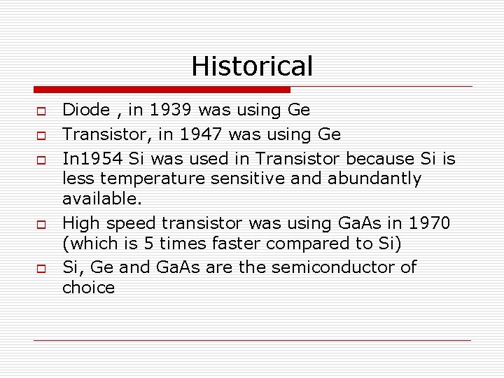
Historical o o o Diode , in 1939 was using Ge Transistor, in 1947 was using Ge In 1954 Si was used in Transistor because Si is less temperature sensitive and abundantly available. High speed transistor was using Ga. As in 1970 (which is 5 times faster compared to Si) Si, Ge and Ga. As are the semiconductor of choice

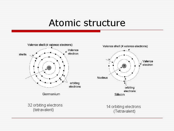
Atomic structure 32 orbiting electrons (tetravalent) 14 orbiting electrons (Tetravalent)

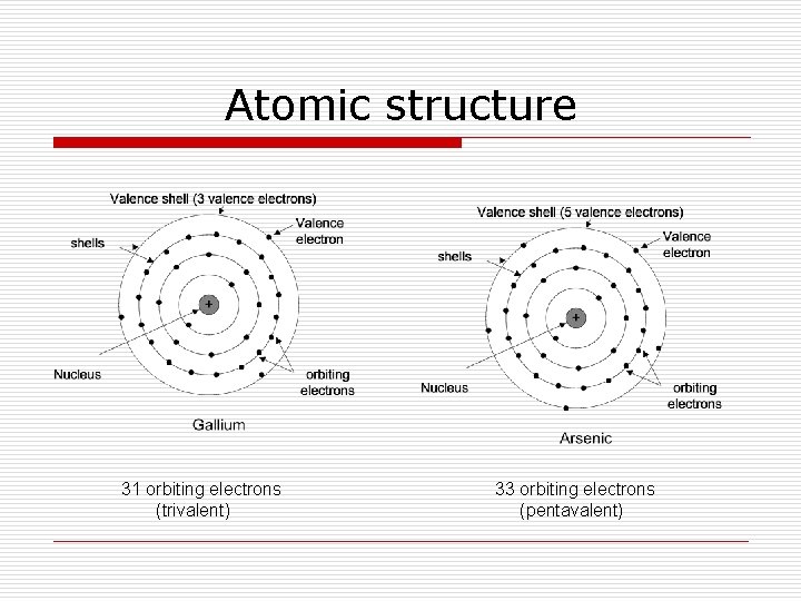
Atomic structure 31 orbiting electrons (trivalent) 33 orbiting electrons (pentavalent)

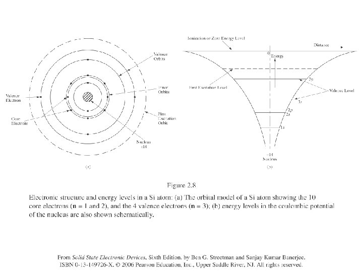
ENERGY LEVELS o o o Each and every isolated electron has a specific energy level associated with shell and orbiting electron. The farther an electron from the nucleus, the higher is the energy state. Electron left its parent atom has a higher energy state than any electron in the atomic structure.

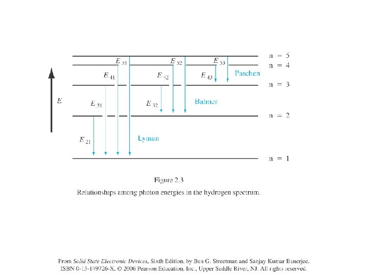
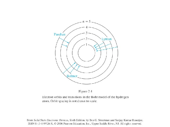
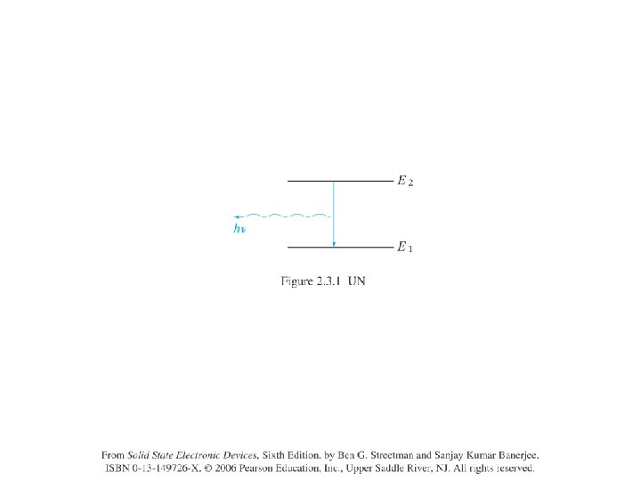
Band Theory o Analogy to atoms –From chemistry, we are familiar with the idea of “electron clouds” orbiting the nucleus. –The energy of the different clouds, or levels, is discrete. Adding energy can cause an electron to “jump” into a higher level. In the same way, an electron can lose energy and emit a specific wavelength of light when falling to a lower energy level. (Atomic spectra) –Pauli Exclusion Principle: no two electrons can occupy the same exact state at the same time. This is why electrons fill the energy levels in the way they do. –Valence electrons are the electrons bound farthest from the nucleus


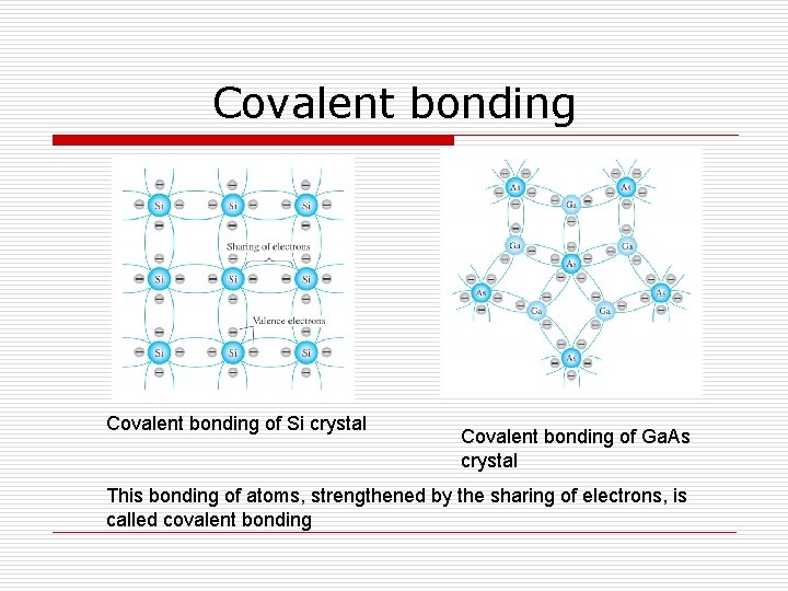
Covalent bonding of Si crystal Covalent bonding of Ga. As crystal This bonding of atoms, strengthened by the sharing of electrons, is called covalent bonding

Exercise 1 o o o Name the materials that suitable for electronic devices What are the advantages and disadvantages of each materials? What is a covalent bonding? Describe it.

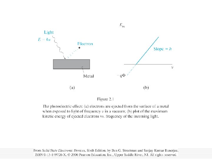
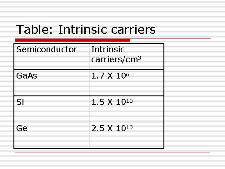
Free state Energy from external natural cause the valence electrons to absorb sufficient kinetic energy and break the covalent bond. This is assume to be free state. o Electron that has separated from the fixed lattice structure is called free carriers. o At room temperature, approximately 1. 5 X 10¹⁰ free carriers in 1 cm 3 of intrinsic silicon material *intrinsic means material has been refined to a very low level of impurities. o


Table: Intrinsic carriers Semiconductor Intrinsic carriers/cm 3 Ga. As 1. 7 X 10⁶ Si 1. 5 X 10¹⁰ Ge 2. 5 X 10¹³

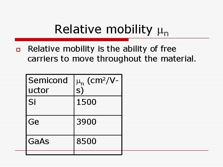
Relative mobility mn o Relative mobility is the ability of free carriers to move throughout the material. Semicond uctor Si mn (cm 2/Vs) 1500 Ge 3900 Ga. As 8500

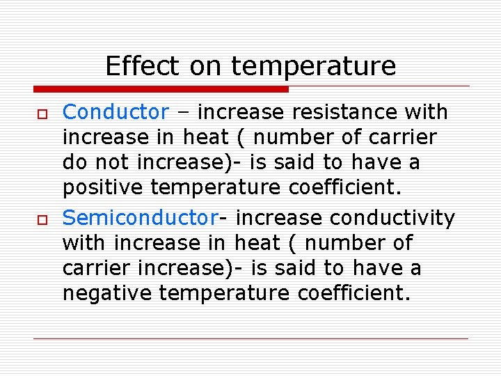
Effect on temperature o o Conductor – increase resistance with increase in heat ( number of carrier do not increase)- is said to have a positive temperature coefficient. Semiconductor- increase conductivity with increase in heat ( number of carrier increase)- is said to have a negative temperature coefficient.

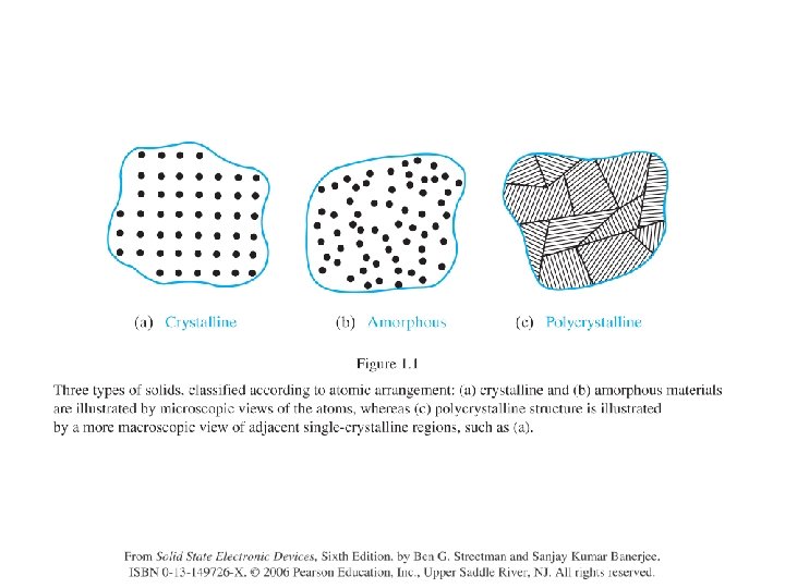
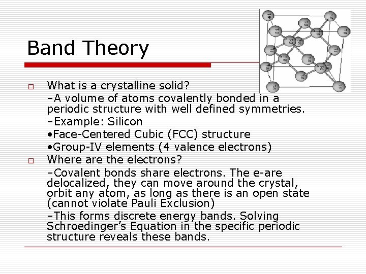
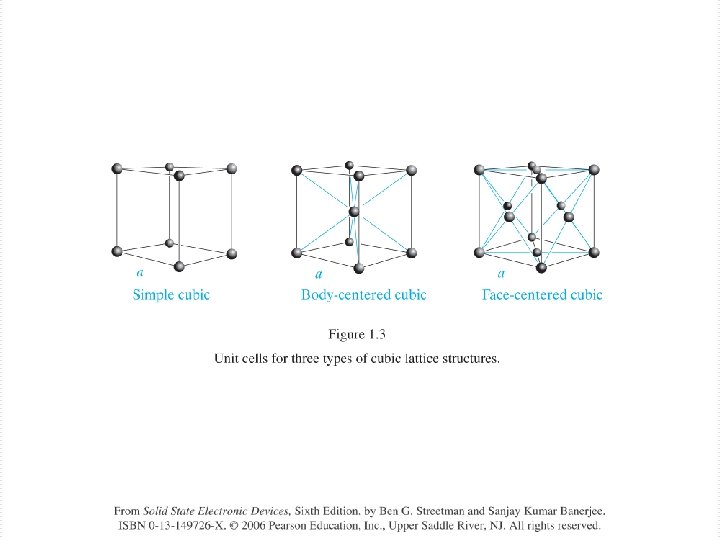
Band Theory o o What is a crystalline solid? –A volume of atoms covalently bonded in a periodic structure with well defined symmetries. –Example: Silicon • Face-Centered Cubic (FCC) structure • Group-IV elements (4 valence electrons) Where are the electrons? –Covalent bonds share electrons. The e-are delocalized, they can move around the crystal, orbit any atom, as long as there is an open state (cannot violate Pauli Exclusion) –This forms discrete energy bands. Solving Schroedinger’s Equation in the specific periodic structure reveals these bands.

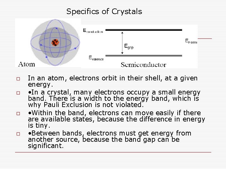
Specifics of Crystals o o In an atom, electrons orbit in their shell, at a given energy. • In a crystal, many electrons occupy a small energy band. There is a width to the energy band, which is why Pauli Exclusion is not violated. • Within the band, electrons can move easily if there available states, because the difference in energy is tiny. • Between bands, electrons must get energy from another source, because the band gap can be significant.


Fermi Energy o The highest energy an electron reached if you were to fill the solid with the intrinsic number of electrons at absolute zero. (No added thermal energy) • Meaningful! There is a sea of electrons sitting beneath this energy. –If you bring two solids together with different Fermi energies, the electrons will move around to reach an equilibrium. (Foreshadowing: PN junction) –If you try to put a lower energy electron into a solid (at absolute zero) with a higher Fermi energy, it won’t fit. It cannot be done due to Pauli Exclusion. • If the highest energy electron exactly fills a band, the Fermi Energy is near the center of the bands.


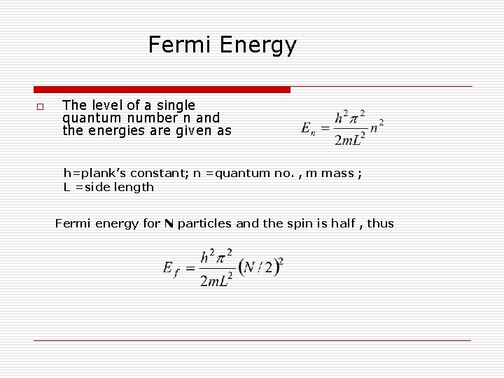
Fermi Energy o The level of a single quantum number n and the energies are given as h=plank’s constant; n =quantum no. , m mass ; L =side length Fermi energy for N particles and the spin is half , thus

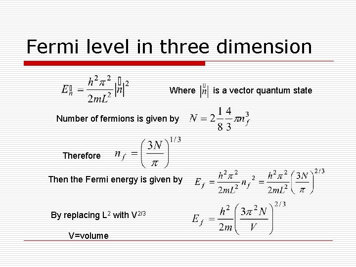
Fermi level in three dimension Where Number of fermions is given by Therefore Then the Fermi energy is given by By replacing L 2 with V 2/3 V=volume is a vector quantum state

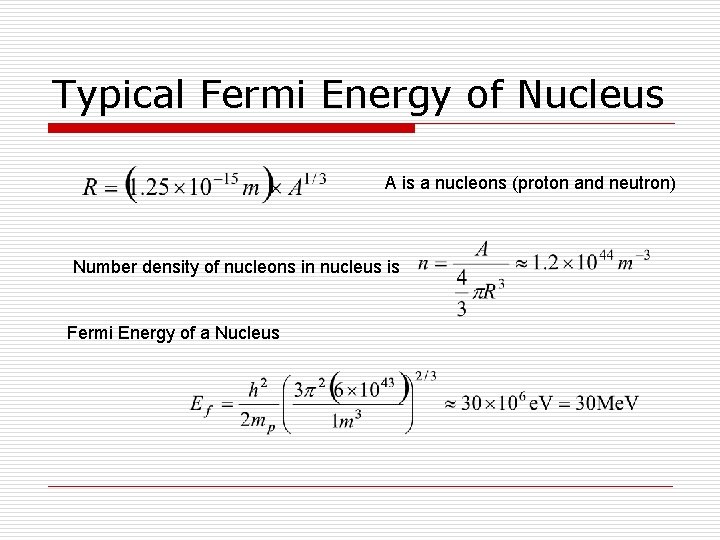
Typical Fermi Energy of Nucleus A is a nucleons (proton and neutron) Number density of nucleons in nucleus is Fermi Energy of a Nucleus

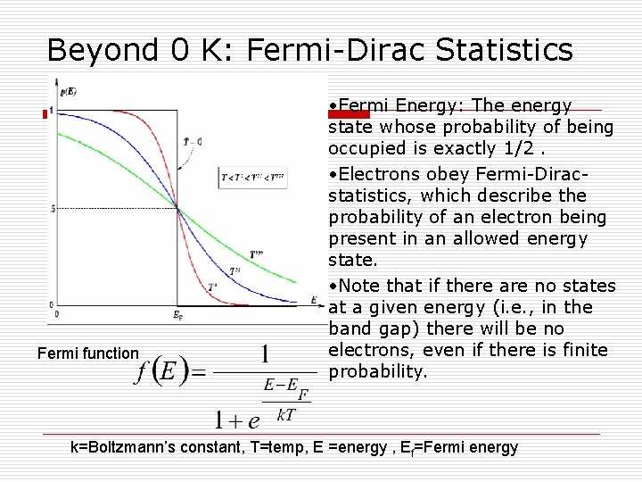
Beyond 0 K: Fermi-Dirac Statistics Fermi function • Fermi Energy: The energy state whose probability of being occupied is exactly 1/2. • Electrons obey Fermi-Diracstatistics, which describe the probability of an electron being present in an allowed energy state. • Note that if there are no states at a given energy (i. e. , in the band gap) there will be no electrons, even if there is finite probability. k=Boltzmann’s constant, T=temp, E =energy , Ef=Fermi energy

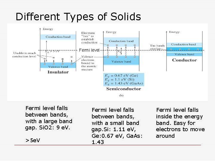
Different Types of Solids Fermi level falls between bands, with a large band gap. Si. O 2: 9 e. V. >5 e. V Fermi level falls between bands, with a small band gap. Si: 1. 11 e. V, Ge: 0. 67 e. V, Ga. As: 1. 43 Fermi level falls inside the energy band. Easy for electrons to move around

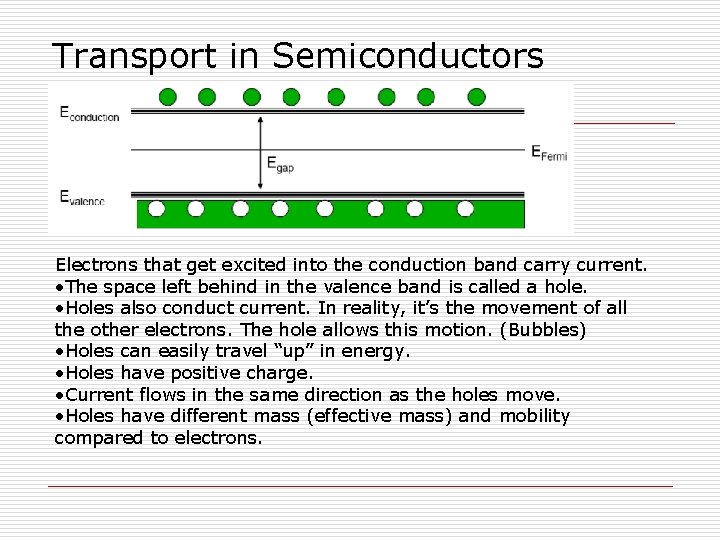
Transport in Semiconductors Electrons that get excited into the conduction band carry current. • The space left behind in the valence band is called a hole. • Holes also conduct current. In reality, it’s the movement of all the other electrons. The hole allows this motion. (Bubbles) • Holes can easily travel “up” in energy. • Holes have positive charge. • Current flows in the same direction as the holes move. • Holes have different mass (effective mass) and mobility compared to electrons.

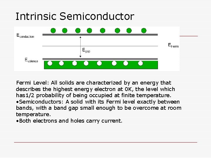
Intrinsic Semiconductor Fermi Level: All solids are characterized by an energy that describes the highest energy electron at 0 K, the level which has 1/2 probability of being occupied at finite temperature. • Semiconductors: A solid with its Fermi level exactly between bands, with a band gap small enough to be overcome at room temperature. • Both electrons and holes carry current.

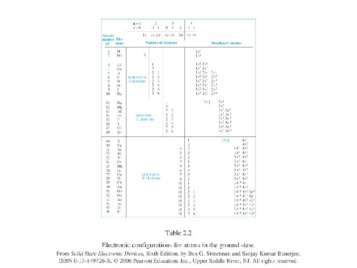
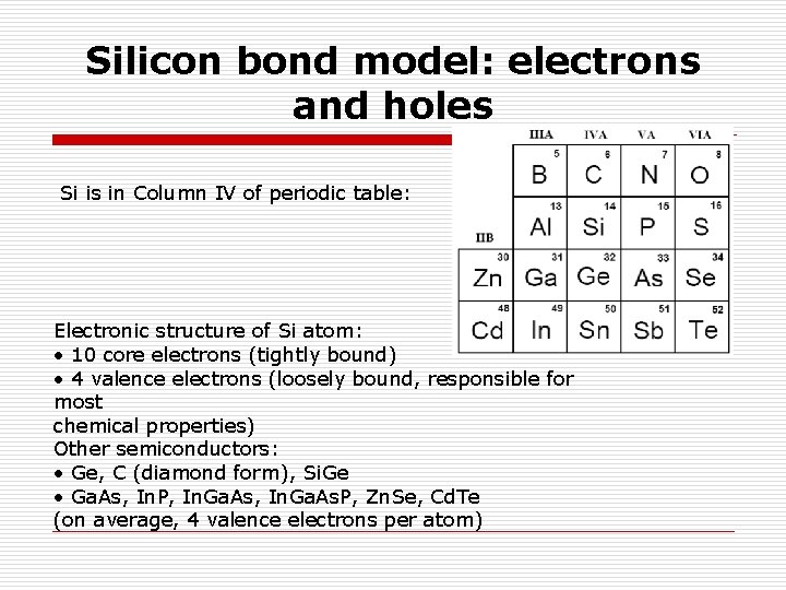
Silicon bond model: electrons and holes Si is in Column IV of periodic table: Electronic structure of Si atom: • 10 core electrons (tightly bound) • 4 valence electrons (loosely bound, responsible for most chemical properties) Other semiconductors: • Ge, C (diamond form), Si. Ge • Ga. As, In. P, In. Ga. As. P, Zn. Se, Cd. Te (on average, 4 valence electrons per atom)

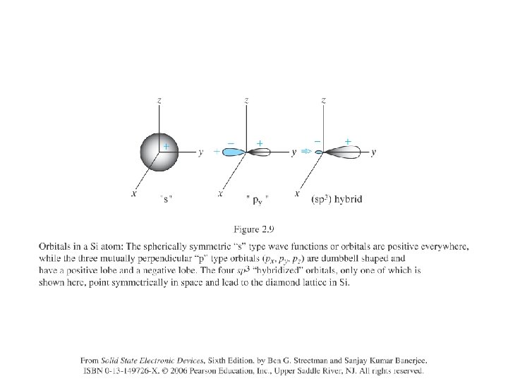
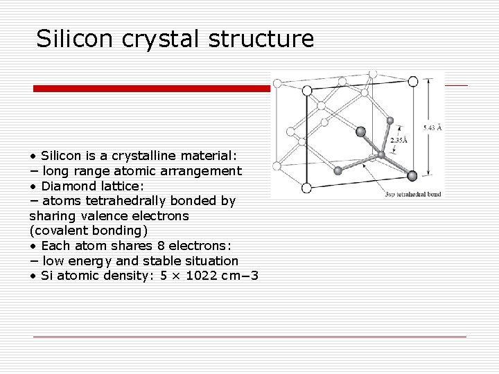
Silicon crystal structure • Silicon is a crystalline material: – long range atomic arrangement • Diamond lattice: – atoms tetrahedrally bonded by sharing valence electrons (covalent bonding) • Each atom shares 8 electrons: – low energy and stable situation • Si atomic density: 5 × 1022 cm− 3

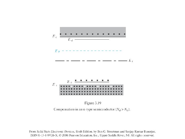
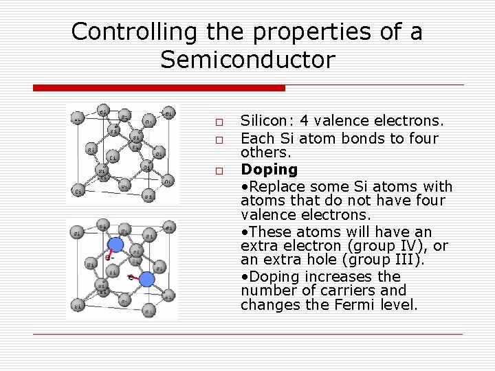
Controlling the properties of a Semiconductor o o o Silicon: 4 valence electrons. Each Si atom bonds to four others. Doping • Replace some Si atoms with atoms that do not have four valence electrons. • These atoms will have an extra electron (group IV), or an extra hole (group III). • Doping increases the number of carriers and changes the Fermi level.

Extrinsic materials o o A semiconductor material that has been subjected to the doping process is called an extrinsic material. Type of materials n n n-type p-type

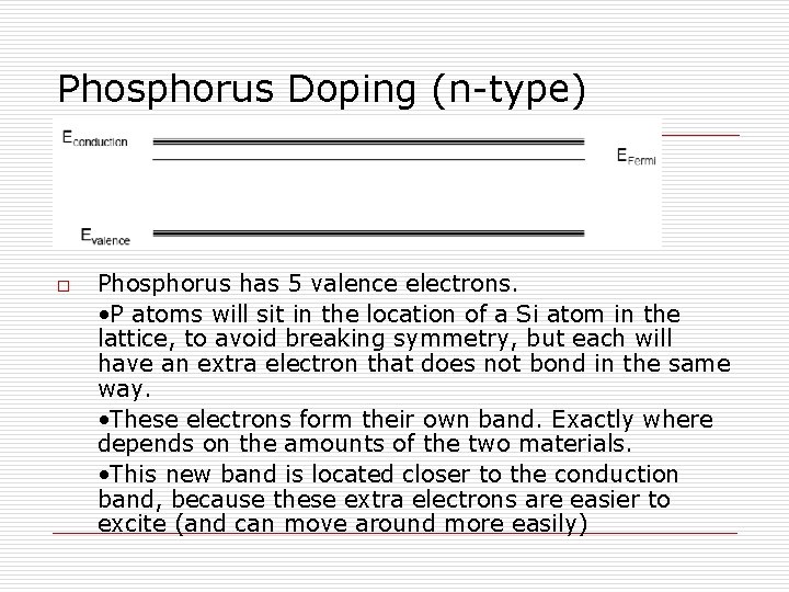
Phosphorus Doping (n-type) o Phosphorus has 5 valence electrons. • P atoms will sit in the location of a Si atom in the lattice, to avoid breaking symmetry, but each will have an extra electron that does not bond in the same way. • These electrons form their own band. Exactly where depends on the amounts of the two materials. • This new band is located closer to the conduction band, because these extra electrons are easier to excite (and can move around more easily)

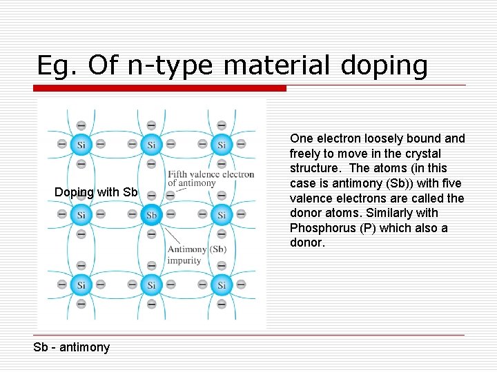
Eg. Of n-type material doping Doping with Sb Sb - antimony One electron loosely bound and freely to move in the crystal structure. The atoms (in this case is antimony (Sb)) with five valence electrons are called the donor atoms. Similarly with Phosphorus (P) which also a donor.

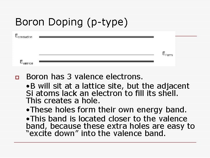
Boron Doping (p-type) o Boron has 3 valence electrons. • B will sit at a lattice site, but the adjacent Si atoms lack an electron to fill its shell. This creates a hole. • These holes form their own energy band. • This band is located closer to the valence band, because these extra holes are easy to “excite down” into the valence band.

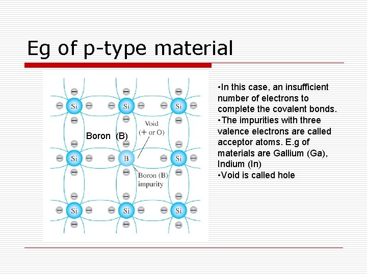
Eg of p-type material Boron (B) • In this case, an insufficient number of electrons to complete the covalent bonds. • The impurities with three valence electrons are called acceptor atoms. E. g of materials are Gallium (Ga), Indium (In) • Void is called hole

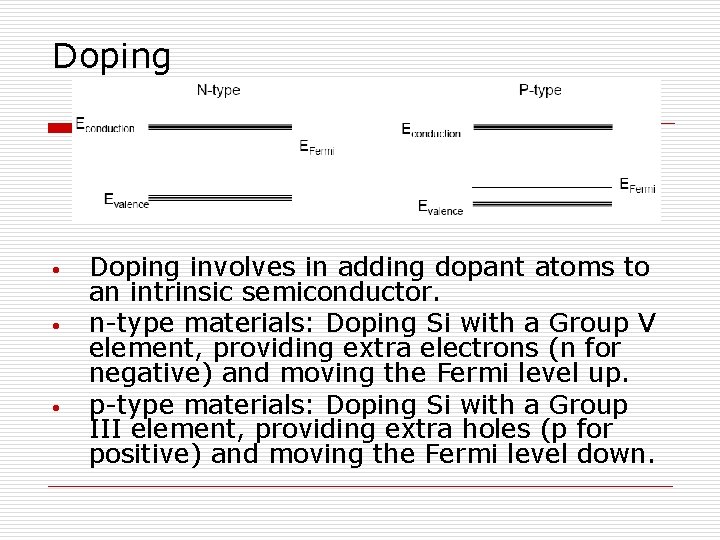
Doping • • • Doping involves in adding dopant atoms to an intrinsic semiconductor. n-type materials: Doping Si with a Group V element, providing extra electrons (n for negative) and moving the Fermi level up. p-type materials: Doping Si with a Group III element, providing extra holes (p for positive) and moving the Fermi level down.

Dopant o o Group V (n-type) –usually antimony(Sb), arsenic(A), phosphorus(P) Group III (p-type)-usually Boron(B) , Gallium (Ga) and Indium (In)

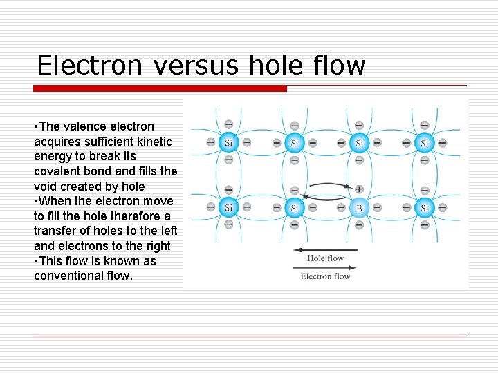
Electron versus hole flow • The valence electron acquires sufficient kinetic energy to break its covalent bond and fills the void created by hole • When the electron move to fill the hole therefore a transfer of holes to the left and electrons to the right • This flow is known as conventional flow.

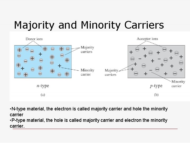
Majority and Minority Carriers • N-type material, the electron is called majority carrier and hole the minority carrier • P-type material, the hole is called majority carrier and electron the minority carrier.

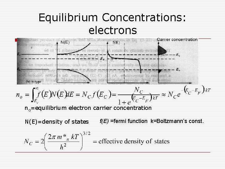
Equilibrium Concentrations: electrons no=equilibrium electron carrier concentration N(E)=density of states f(E) =fermi function k=Boltzmann’s const.

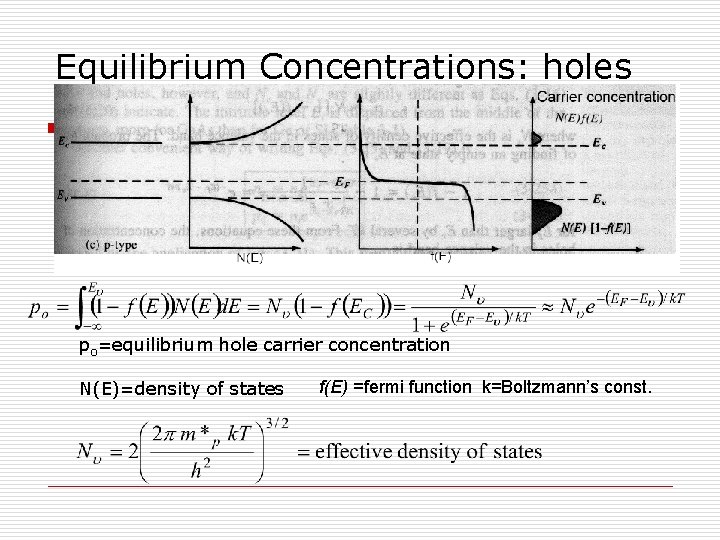
Equilibrium Concentrations: holes po=equilibrium hole carrier concentration N(E)=density of states f(E) =fermi function k=Boltzmann’s const.

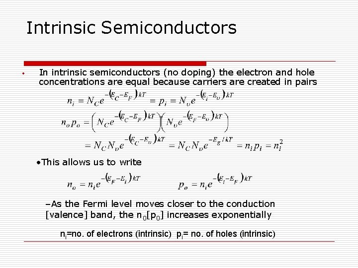
Intrinsic Semiconductors • In intrinsic semiconductors (no doping) the electron and hole concentrations are equal because carriers are created in pairs • This allows us to write –As the Fermi level moves closer to the conduction [valence] band, the n 0[p 0] increases exponentially ni=no. of electrons (intrinsic) pi= no. of holes (intrinsic)

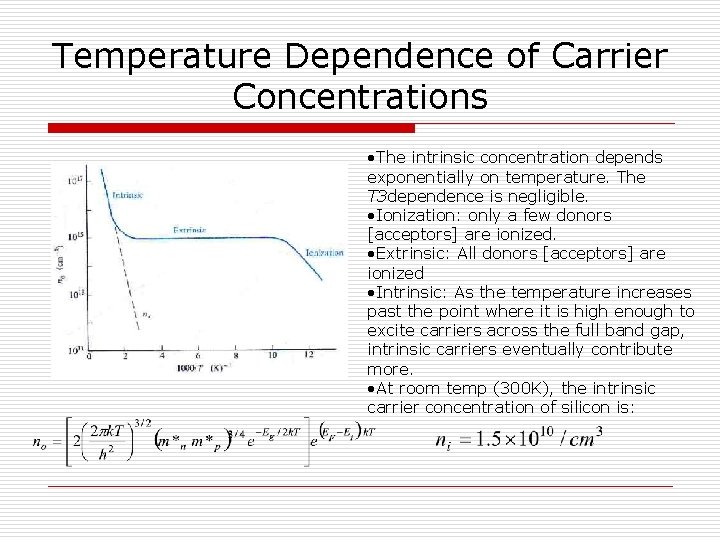
Temperature Dependence of Carrier Concentrations • The intrinsic concentration depends exponentially on temperature. The T 3 dependence is negligible. • Ionization: only a few donors [acceptors] are ionized. • Extrinsic: All donors [acceptors] are ionized • Intrinsic: As the temperature increases past the point where it is high enough to excite carriers across the full band gap, intrinsic carriers eventually contribute more. • At room temp (300 K), the intrinsic carrier concentration of silicon is:

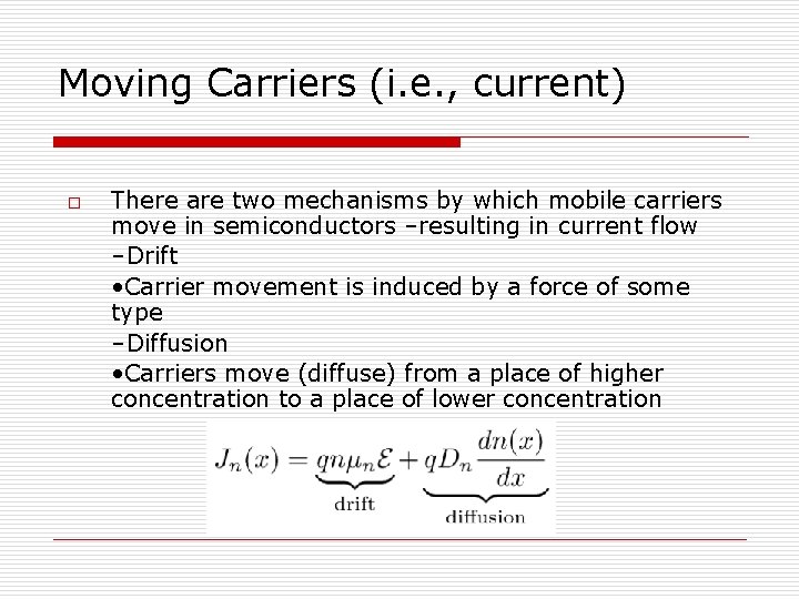
Moving Carriers (i. e. , current) o There are two mechanisms by which mobile carriers move in semiconductors –resulting in current flow –Drift • Carrier movement is induced by a force of some type –Diffusion • Carriers move (diffuse) from a place of higher concentration to a place of lower concentration

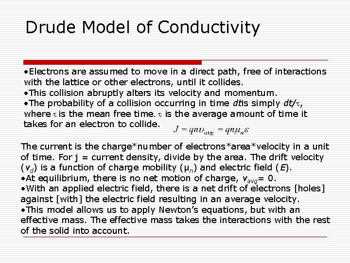
Drude Model of Conductivity • Electrons are assumed to move in a direct path, free of interactions with the lattice or other electrons, until it collides. • This collision abruptly alters its velocity and momentum. • The probability of a collision occurring in time dtis simply dt/t, where t is the mean free time. t is the average amount of time it takes for an electron to collide. The current is the charge*number of electrons*area*velocity in a unit of time. For j = current density, divide by the area. The drift velocity (vd) is a function of charge mobility (μn) and electric field (E). • At equilibrium, there is no net motion of charge, vavg= 0. • With an applied electric field, there is a net drift of electrons [holes] against [with] the electric field resulting in an average velocity. • This model allows us to apply Newton’s equations, but with an effective mass. The effective mass takes the interactions with the rest of the solid into account.

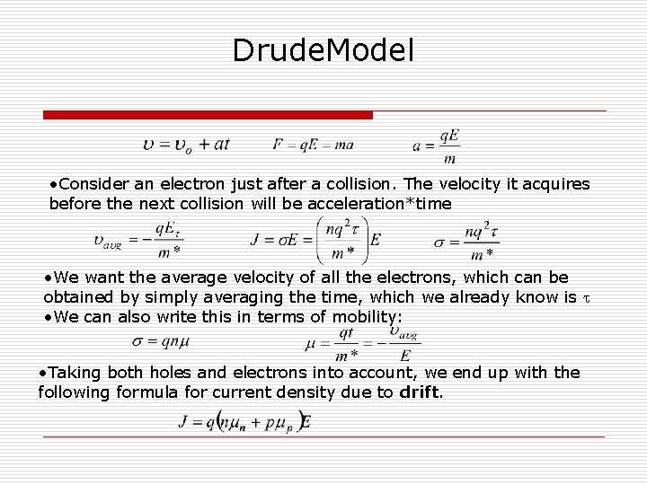
Drude. Model • Consider an electron just after a collision. The velocity it acquires before the next collision will be acceleration*time • We want the average velocity of all the electrons, which can be obtained by simply averaging the time, which we already know is t • We can also write this in terms of mobility: • Taking both holes and electrons into account, we end up with the following formula for current density due to drift.

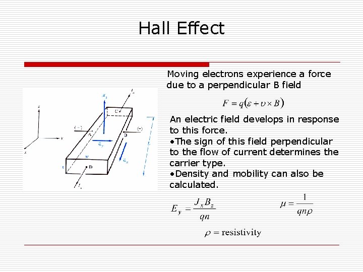
Hall Effect Moving electrons experience a force due to a perpendicular B field An electric field develops in response to this force. • The sign of this field perpendicular to the flow of current determines the carrier type. • Density and mobility can also be calculated.

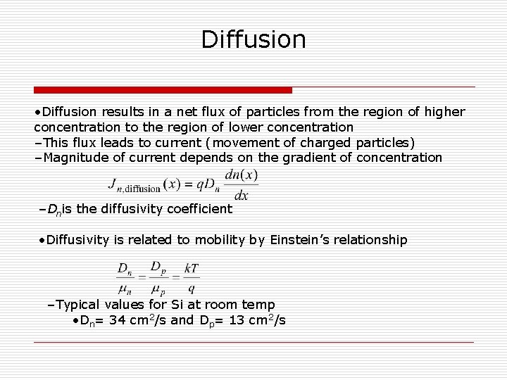
Diffusion • Diffusion results in a net flux of particles from the region of higher concentration to the region of lower concentration –This flux leads to current (movement of charged particles) –Magnitude of current depends on the gradient of concentration –Dnis the diffusivity coefficient • Diffusivity is related to mobility by Einstein’s relationship –Typical values for Si at room temp • Dn= 34 cm 2/s and Dp= 13 cm 2/s