EECS 252 Graduate Computer Architecture Lec 23 Storage

![Avoiding Bank Conflicts • Lots of banks int x[256][512]; for (j = 0; j Avoiding Bank Conflicts • Lots of banks int x[256][512]; for (j = 0; j](https://slidetodoc.com/presentation_image/00b7b9b17cd884decf9abcda4f6114f7/image-11.jpg)


- Slides: 81

EECS 252 Graduate Computer Architecture Lec 23 – Storage Technology David Culler Electrical Engineering and Computer Sciences University of California, Berkeley http: //www. eecs. berkeley. edu/~culler http: //www inst. eecs. berkeley. edu/~cs 252

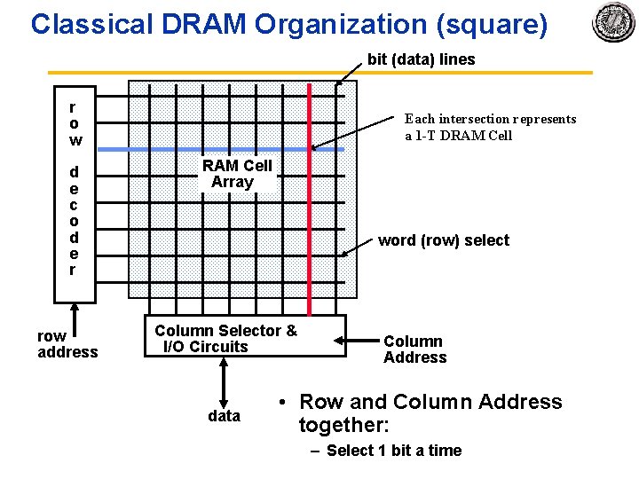
Classical DRAM Organization (square) bit (data) lines r o w d e c o d e r row address Each intersection represents a 1 -T DRAM Cell Array word (row) select Column Selector & I/O Circuits data Column Address • Row and Column Address together: – Select 1 bit a time

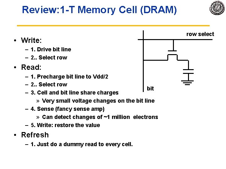
Review: 1 T Memory Cell (DRAM) • Write: – 1. Drive bit line – 2. . Select row • Read: – 1. Precharge bit line to Vdd/2 – 2. . Select row bit – 3. Cell and bit line share charges » Very small voltage changes on the bit line – 4. Sense (fancy sense amp) » Can detect changes of ~1 million electrons – 5. Write: restore the value • Refresh – 1. Just do a dummy read to every cell. row select

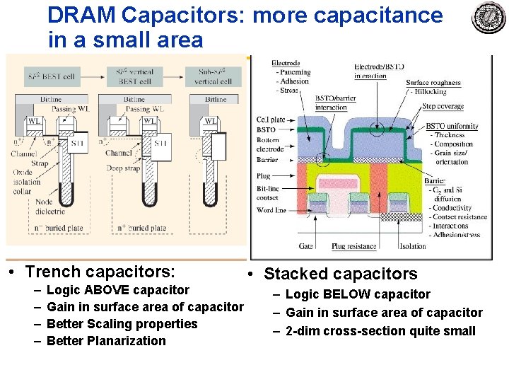
DRAM Capacitors: more capacitance in a small area • Trench capacitors: – – Logic ABOVE capacitor Gain in surface area of capacitor Better Scaling properties Better Planarization • Stacked capacitors – Logic BELOW capacitor – Gain in surface area of capacitor – 2 dim cross section quite small

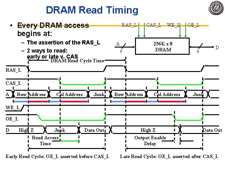
DRAM Read Timing • Every DRAM access begins at: RAS_L – The assertion of the RAS_L – 2 ways to read: early or late v. CAS A CAS_L WE_L 256 K x 8 DRAM 9 OE_L D 8 DRAM Read Cycle Time RAS_L CAS_L A Row Address Col Address Junk WE_L OE_L D High Z Junk Read Access Time Data Out Early Read Cycle: OE_L asserted before CAS_L High Z Output Enable Delay Data Out Late Read Cycle: OE_L asserted after CAS_L

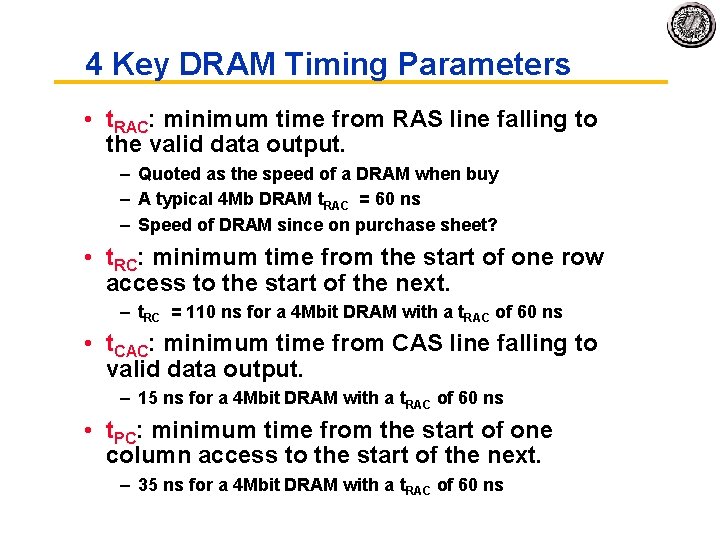
4 Key DRAM Timing Parameters • t. RAC: minimum time from RAS line falling to the valid data output. – Quoted as the speed of a DRAM when buy – A typical 4 Mb DRAM t. RAC = 60 ns – Speed of DRAM since on purchase sheet? • t. RC: minimum time from the start of one row access to the start of the next. – t. RC = 110 ns for a 4 Mbit DRAM with a t. RAC of 60 ns • t. CAC: minimum time from CAS line falling to valid data output. – 15 ns for a 4 Mbit DRAM with a t. RAC of 60 ns • t. PC: minimum time from the start of one column access to the start of the next. – 35 ns for a 4 Mbit DRAM with a t. RAC of 60 ns

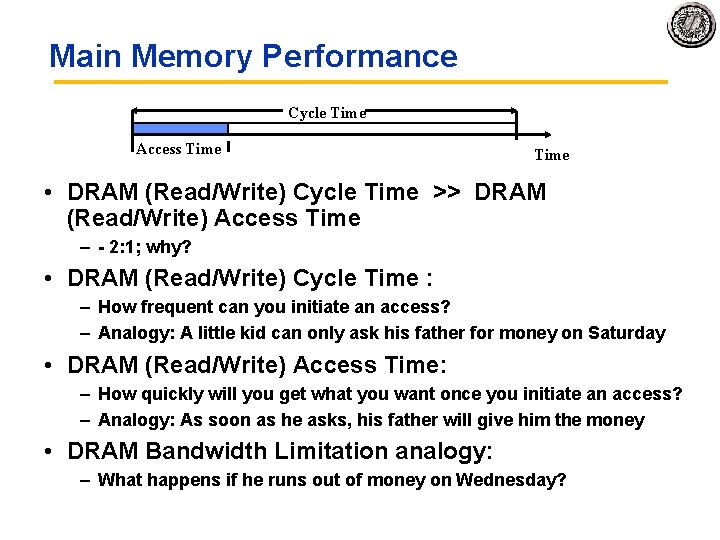
Main Memory Performance Cycle Time Access Time • DRAM (Read/Write) Cycle Time >> DRAM (Read/Write) Access Time – 2: 1; why? • DRAM (Read/Write) Cycle Time : – How frequent can you initiate an access? – Analogy: A little kid can only ask his father for money on Saturday • DRAM (Read/Write) Access Time: – How quickly will you get what you want once you initiate an access? – Analogy: As soon as he asks, his father will give him the money • DRAM Bandwidth Limitation analogy: – What happens if he runs out of money on Wednesday?

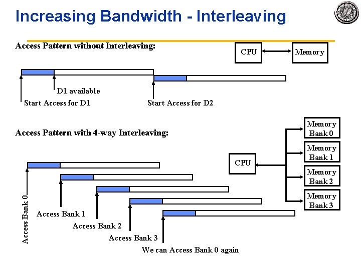
Increasing Bandwidth Interleaving Access Pattern without Interleaving: D 1 available Start Access for D 1 CPU Memory Start Access for D 2 Memory Bank 0 Access Pattern with 4 -way Interleaving: CPU Memory Bank 1 Access Bank 0 Memory Bank 2 Access Bank 1 Access Bank 2 Access Bank 3 We can Access Bank 0 again Memory Bank 3

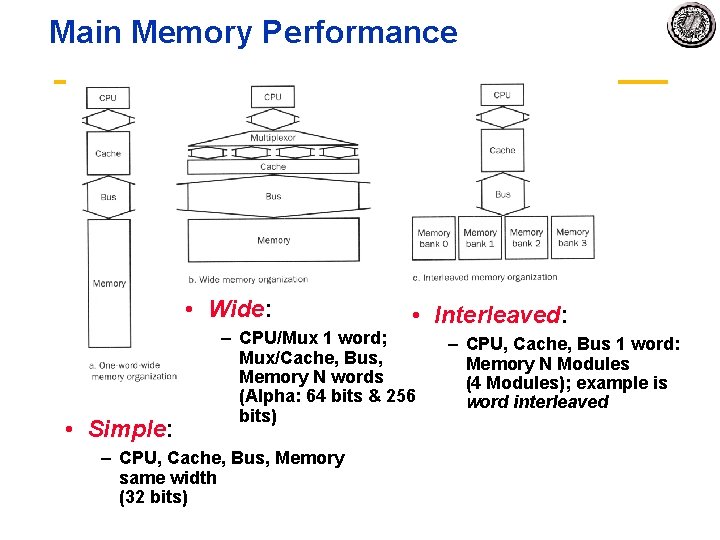
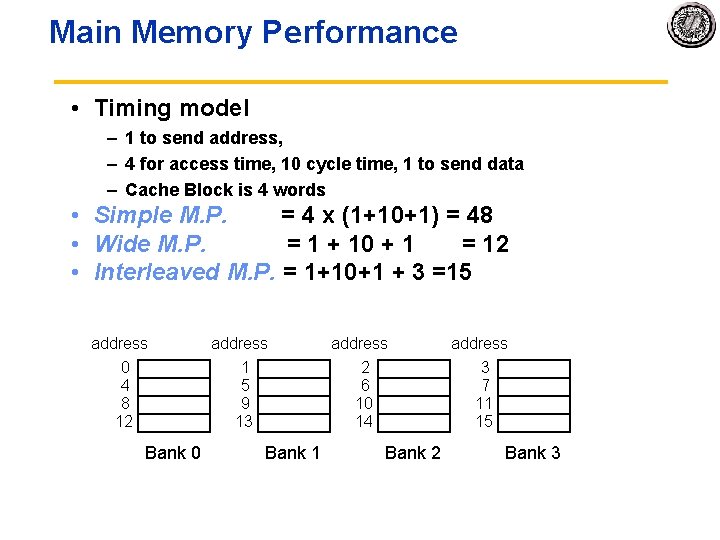
Main Memory Performance • Wide: • Simple: • Interleaved: – CPU/Mux 1 word; Mux/Cache, Bus, Memory N words (Alpha: 64 bits & 256 bits) – CPU, Cache, Bus, Memory same width (32 bits) – CPU, Cache, Bus 1 word: Memory N Modules (4 Modules); example is word interleaved

Main Memory Performance • Timing model – 1 to send address, – 4 for access time, 10 cycle time, 1 to send data – Cache Block is 4 words • Simple M. P. = 4 x (1+10+1) = 48 • Wide M. P. = 1 + 10 + 1 = 12 • Interleaved M. P. = 1+10+1 + 3 =15 address 0 4 8 12 Bank 0 address 1 5 9 13 Bank 1 address 2 6 10 14 3 7 11 15 Bank 2 Bank 3
![Avoiding Bank Conflicts Lots of banks int x256512 for j 0 j Avoiding Bank Conflicts • Lots of banks int x[256][512]; for (j = 0; j](https://slidetodoc.com/presentation_image/00b7b9b17cd884decf9abcda4f6114f7/image-11.jpg)
Avoiding Bank Conflicts • Lots of banks int x[256][512]; for (j = 0; j < 512; j = j+1) for (i = 0; i < 256; i = i+1) x[i][j] = 2 * x[i][j]; • Even with 128 banks, since 512 is multiple of 128, conflict on word accesses • SW: loop interchange or declaring array not power of 2 (“array padding”) • HW: Prime number of banks – – bank number = address mod number of banks address within bank = address / number of words in bank modulo & divide per memory access with prime no. banks?

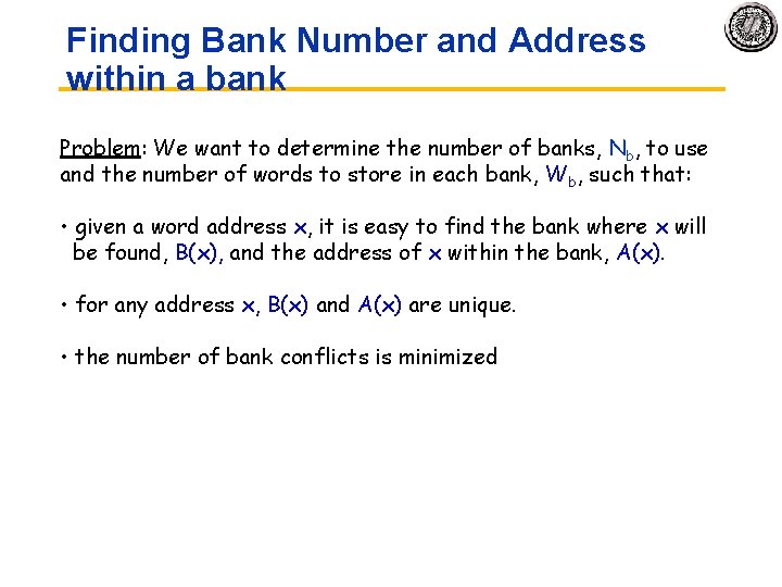
Finding Bank Number and Address within a bank Problem: We want to determine the number of banks, Nb, to use and the number of words to store in each bank, Wb, such that: • given a word address x, it is easy to find the bank where x will be found, B(x), and the address of x within the bank, A(x). • for any address x, B(x) and A(x) are unique. • the number of bank conflicts is minimized

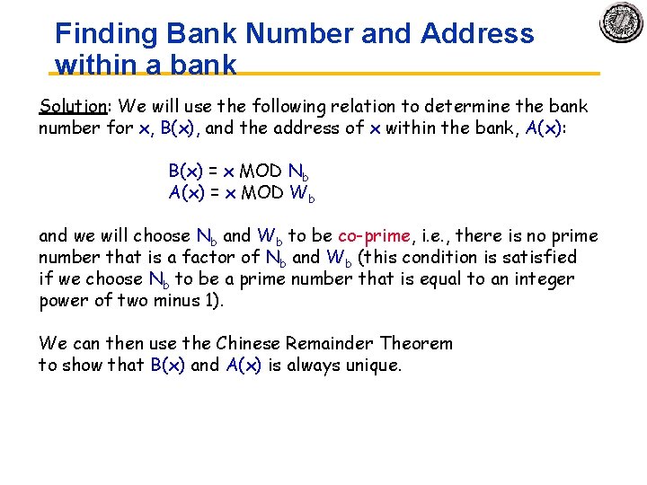
Finding Bank Number and Address within a bank Solution: We will use the following relation to determine the bank number for x, B(x), and the address of x within the bank, A(x): B(x) = x MOD Nb A(x) = x MOD Wb and we will choose Nb and Wb to be co-prime, i. e. , there is no prime number that is a factor of Nb and Wb (this condition is satisfied if we choose Nb to be a prime number that is equal to an integer power of two minus 1). We can then use the Chinese Remainder Theorem to show that B(x) and A(x) is always unique.

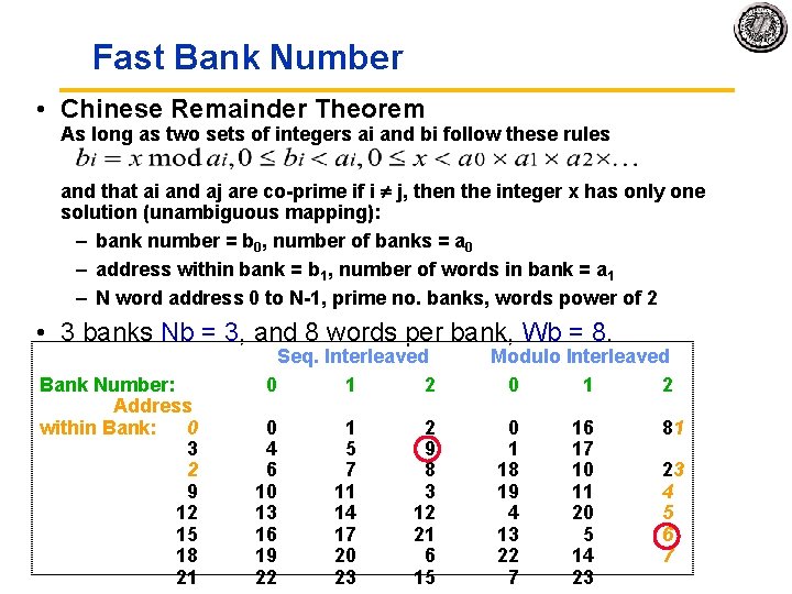
Fast Bank Number • Chinese Remainder Theorem As long as two sets of integers ai and bi follow these rules and that ai and aj are co prime if i j, then the integer x has only one solution (unambiguous mapping): – bank number = b 0, number of banks = a 0 – address within bank = b 1, number of words in bank = a 1 – N word address 0 to N 1, prime no. banks, words power of 2 • 3 banks Nb = 3, and 8 words per bank, Wb = 8. Bank Number: Address within Bank: 0 3 2 9 12 15 18 21 Seq. Interleaved Modulo Interleaved 0 1 2 0 4 6 10 13 16 19 22 1 5 7 11 14 17 20 23 2 9 8 3 12 21 6 15 0 1 18 19 4 13 22 7 16 17 10 11 20 5 14 23 81 23 4 5 6 7

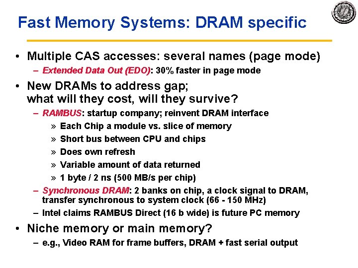
Fast Memory Systems: DRAM specific • Multiple CAS accesses: several names (page mode) – Extended Data Out (EDO): 30% faster in page mode • New DRAMs to address gap; what will they cost, will they survive? – RAMBUS: startup company; reinvent DRAM interface » Each Chip a module vs. slice of memory » Short bus between CPU and chips » Does own refresh » Variable amount of data returned » 1 byte / 2 ns (500 MB/s per chip) – Synchronous DRAM: 2 banks on chip, a clock signal to DRAM, transfer synchronous to system clock (66 150 MHz) – Intel claims RAMBUS Direct (16 b wide) is future PC memory • Niche memory or main memory? – e. g. , Video RAM for frame buffers, DRAM + fast serial output

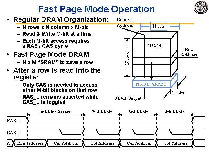
Fast Page Mode Operation • Regular DRAM Organization: – N rows x N column x M bit – Read & Write M bit at a time – Each M bit access requires a RAS / CAS cycle Column Address N cols DRAM – N x M “SRAM” to save a row N rows • Fast Page Mode DRAM Row Address • After a row is read into the register – Only CAS is needed to access other M bit blocks on that row – RAS_L remains asserted while CAS_L is toggled 1 st M-bit Access N x M “SRAM” M bits M-bit Output 2 nd M-bit 3 rd M-bit 4 th M-bit Col Address RAS_L CAS_L A Row Address Col Address

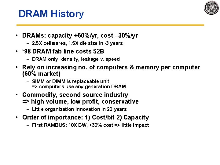
DRAM History • DRAMs: capacity +60%/yr, cost – 30%/yr – 2. 5 X cells/area, 1. 5 X die size in 3 years • ‘ 98 DRAM fab line costs $2 B – DRAM only: density, leakage v. speed • Rely on increasing no. of computers & memory per computer (60% market) – SIMM or DIMM is replaceable unit => computers use any generation DRAM • Commodity, second source industry => high volume, low profit, conservative – Little organization innovation in 20 years • Order of importance: 1) Cost/bit 2) Capacity – First RAMBUS: 10 X BW, +30% cost => little impact

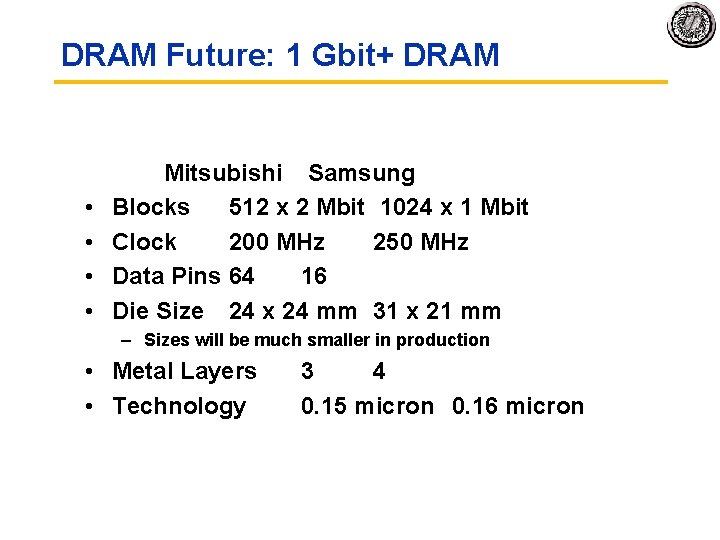
DRAM Future: 1 Gbit+ DRAM • • Mitsubishi Samsung Blocks 512 x 2 Mbit 1024 x 1 Mbit Clock 200 MHz 250 MHz Data Pins 64 16 Die Size 24 x 24 mm 31 x 21 mm – Sizes will be much smaller in production • Metal Layers • Technology 3 4 0. 15 micron 0. 16 micron

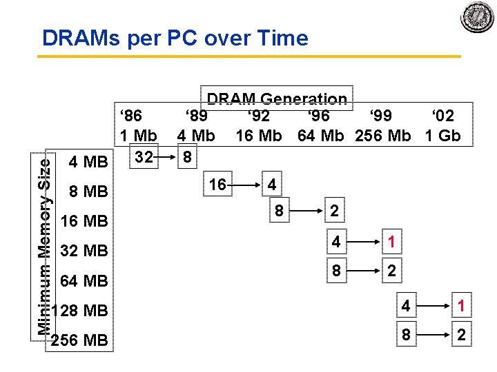
Minimum Memory Size DRAMs per PC over Time DRAM Generation ‘ 86 ‘ 89 ‘ 92 ‘ 96 ‘ 99 ‘ 02 1 Mb 4 Mb 16 Mb 64 Mb 256 Mb 1 Gb 32 8 4 MB 16 4 8 MB 16 MB 32 MB 64 MB 8 2 4 1 8 2 128 MB 4 1 256 MB 8 2

Potential DRAM Crossroads? • After 20 years of 4 X every 3 years, running into wall? (64 Mb 1 Gb) • How can keep $1 B fab lines full if buy fewer DRAMs per computer? • Cost/bit – 30%/yr if stop 4 X/3 yr? • What will happen to $40 B/yr DRAM industry?

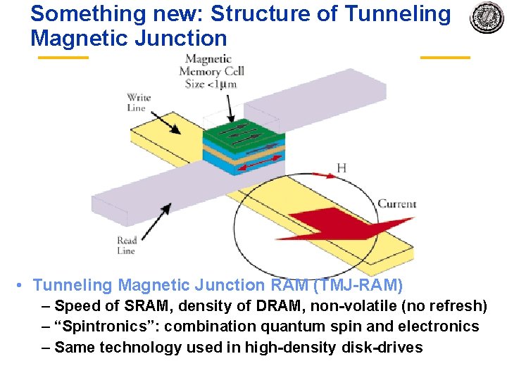
Something new: Structure of Tunneling Magnetic Junction • Tunneling Magnetic Junction RAM (TMJ RAM) – Speed of SRAM, density of DRAM, non volatile (no refresh) – “Spintronics”: combination quantum spin and electronics – Same technology used in high density disk drives

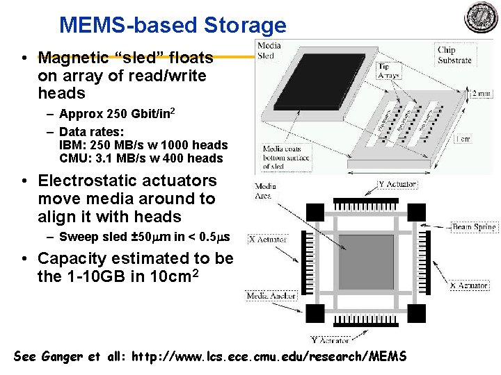
MEMS based Storage • Magnetic “sled” floats on array of read/write heads – Approx 250 Gbit/in 2 – Data rates: IBM: 250 MB/s w 1000 heads CMU: 3. 1 MB/s w 400 heads • Electrostatic actuators move media around to align it with heads – Sweep sled ± 50 m in < 0. 5 s • Capacity estimated to be in the 1 10 GB in 10 cm 2 See Ganger et all: http: //www. lcs. ece. cmu. edu/research/MEMS

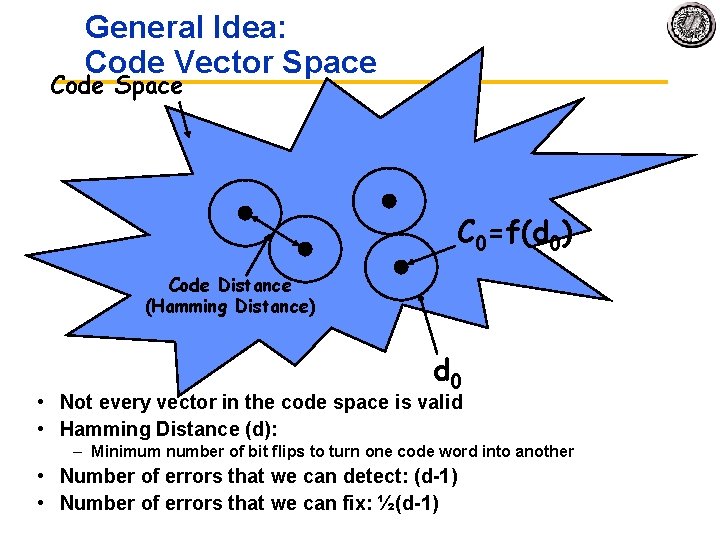
Big storage (such as DRAM/DISK): Potential for Errors! • Motivation: – DRAM is dense Signals are easily disturbed – High Capacity higher probability of failure • Approach: Redundancy – Add extra information so that we can recover from errors – Can we do better than just create complete copies? • Block Codes: Data Coded in blocks – – k data bits coded into n encoded bits Measure of overhead: Rate of Code: K/N Often called an (n, k) code Consider data as vectors in GF(2) [ i. e. vectors of bits ] • Code Space is set of all 2 n vectors, Data space set of 2 k vectors – Encoding function: C=f(d) – Decoding function: d=f(C’) – Not all possible code vectors, C, are valid!

General Idea: Code Vector Space Code Space C 0=f(d 0) Code Distance (Hamming Distance) d 0 • Not every vector in the code space is valid • Hamming Distance (d): – Minimum number of bit flips to turn one code word into another • Number of errors that we can detect: (d 1) • Number of errors that we can fix: ½(d 1)

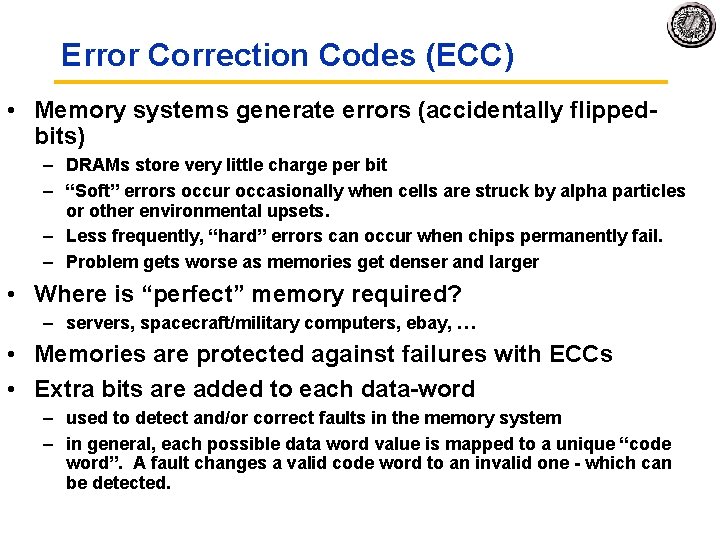
Error Correction Codes (ECC) • Memory systems generate errors (accidentally flipped bits) – DRAMs store very little charge per bit – “Soft” errors occur occasionally when cells are struck by alpha particles or other environmental upsets. – Less frequently, “hard” errors can occur when chips permanently fail. – Problem gets worse as memories get denser and larger • Where is “perfect” memory required? – servers, spacecraft/military computers, ebay, … • Memories are protected against failures with ECCs • Extra bits are added to each data word – used to detect and/or correct faults in the memory system – in general, each possible data word value is mapped to a unique “code word”. A fault changes a valid code word to an invalid one which can be detected.

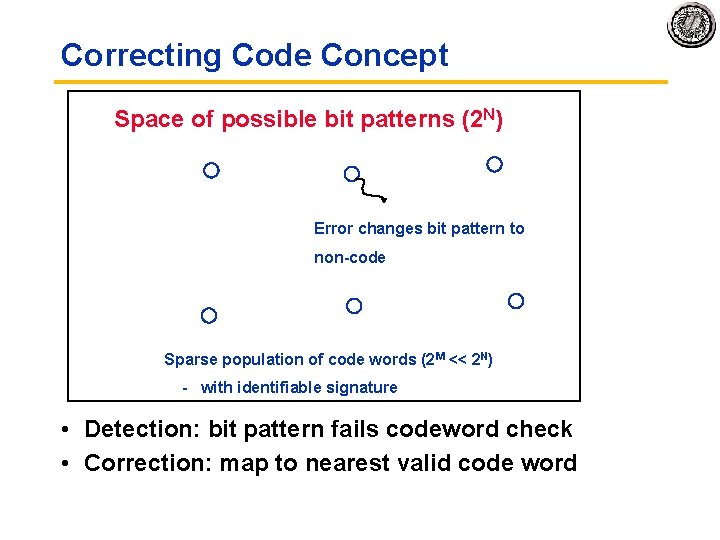
Correcting Code Concept Space of possible bit patterns (2 N) Error changes bit pattern to non code Sparse population of code words (2 M << 2 N) with identifiable signature • Detection: bit pattern fails codeword check • Correction: map to nearest valid code word

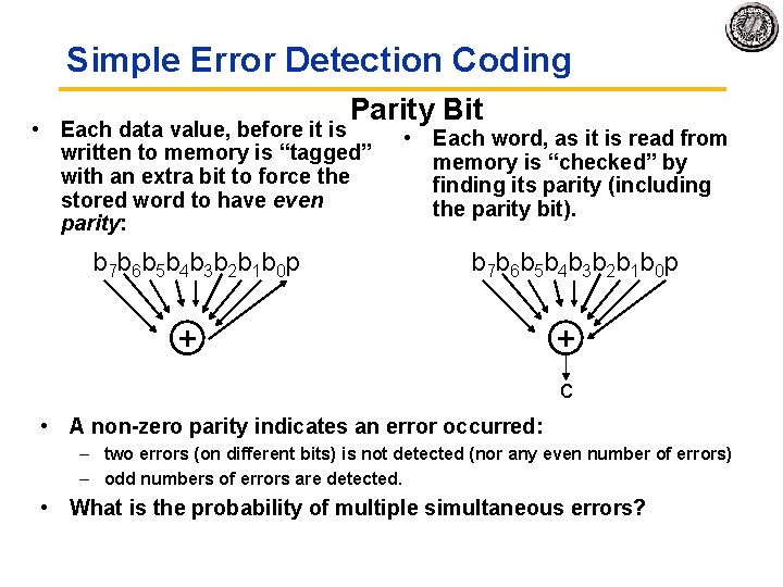
Simple Error Detection Coding Parity Bit • Each data value, before it is written to memory is “tagged” with an extra bit to force the stored word to have even parity: b 7 b 6 b 5 b 4 b 3 b 2 b 1 b 0 p • Each word, as it is read from memory is “checked” by finding its parity (including the parity bit). b 7 b 6 b 5 b 4 b 3 b 2 b 1 b 0 p + + c • A non zero parity indicates an error occurred: – two errors (on different bits) is not detected (nor any even number of errors) – odd numbers of errors are detected. • What is the probability of multiple simultaneous errors?

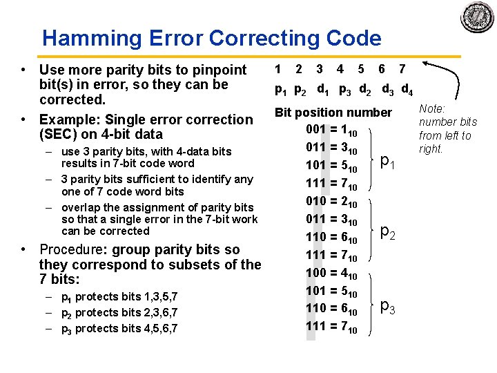
Hamming Error Correcting Code • Use more parity bits to pinpoint bit(s) in error, so they can be corrected. • Example: Single error correction (SEC) on 4 bit data • 1 2 3 4 5 6 7 p 1 p 2 d 1 p 3 d 2 d 3 d 4 Bit position number 001 = 110 011 = 310 – use 3 parity bits, with 4 data bits p 1 results in 7 bit code word 101 = 510 – 3 parity bits sufficient to identify any 111 = 710 one of 7 code word bits 010 = 210 – overlap the assignment of parity bits so that a single error in the 7 bit work 011 = 310 can be corrected p 2 110 = 610 Procedure: group parity bits so 111 = 710 they correspond to subsets of the 100 = 410 7 bits: 101 = 510 – p 1 protects bits 1, 3, 5, 7 p 3 110 = 610 – p 2 protects bits 2, 3, 6, 7 111 = 710 – p 3 protects bits 4, 5, 6, 7 Note: number bits from left to right.

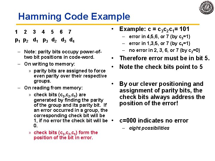
Hamming Code Example 1 2 3 4 5 6 7 p 1 p 2 d 1 p 3 d 2 d 3 d 4 – Note: parity bits occupy power of two bit positions in code word. – On writing to memory: » parity bits are assigned to force even parity over their respective groups. – On reading from memory: » check bits (c 3, c 2, c 1) are generated by finding the parity of the group and its parity bit. If an error occurred in a group, the corresponding check bit will be 1, if no error the check bit will be 0. » check bits (c 3, c 2, c 1) form the position of the bit in error. • Example: c = c 3 c 2 c 1= 101 – error in 4, 5, 6, or 7 (by c 3=1) – error in 1, 3, 5, or 7 (by c 1=1) – no error in 2, 3, 6, or 7 (by c 2=0) • Therefore error must be in bit 5. • Note the check bits point to 5 • By our clever positioning and assignment of parity bits, the check bits always address the position of the error! • c=000 indicates no error – eight possibilities

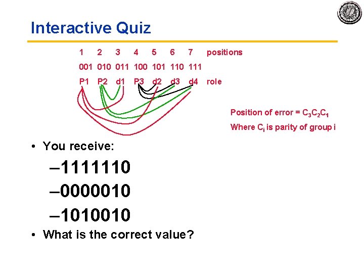
Interactive Quiz 1 2 3 4 5 6 7 positions 001 010 011 100 101 110 111 P 2 d 1 P 3 d 2 d 3 d 4 role Position of error = C 3 C 2 C 1 Where Ci is parity of group i • You receive: – 1111110 – 0000010 – 1010010 • What is the correct value?

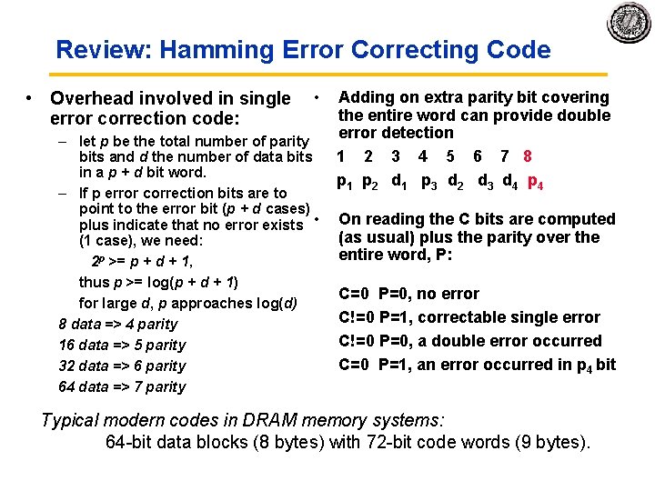
Review: Hamming Error Correcting Code • Overhead involved in single • error correction code: Adding on extra parity bit covering the entire word can provide double error detection – let p be the total number of parity bits and d the number of data bits 1 2 3 4 5 6 7 8 in a p + d bit word. p 1 p 2 d 1 p 3 d 2 d 3 d 4 p 4 – If p error correction bits are to point to the error bit (p + d cases) plus indicate that no error exists • (1 case), we need: 2 p >= p + d + 1, thus p >= log(p + d + 1) for large d, p approaches log(d) 8 data => 4 parity 16 data => 5 parity 32 data => 6 parity 64 data => 7 parity On reading the C bits are computed (as usual) plus the parity over the entire word, P: C=0 P=0, no error C!=0 P=1, correctable single error C!=0 P=0, a double error occurred C=0 P=1, an error occurred in p 4 bit Typical modern codes in DRAM memory systems: 64 -bit data blocks (8 bytes) with 72 -bit code words (9 bytes).

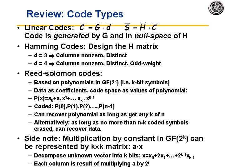
Review: Code Types • Linear Codes: Code is generated by G and in null-space of H • Hamming Codes: Design the H matrix – d = 3 Columns nonzero, Distinct – d = 4 Columns nonzero, Distinct, Odd weight • Reed solomon codes: – – – Based on polynomials in GF(2 k) (I. e. k bit symbols) Data as coefficients, code space as values of polynomial: P(x)=a 0+a 1 x 1+… ak 1 xk 1 Coded: P(0), P(1), P(2)…. , P(n 1) Can recover polynomial as long as get any k of n Alternatively: as long as no more than n k coded symbols erased, can recover data. • Side note: Multiplication by constant in GF(2 k) can be represented by k k matrix: a x – Decompose unknown vector into k bits: x=x 0+2 x 1+…+2 k 1 xk 1 – Each column is result of multiplying a by 2 i

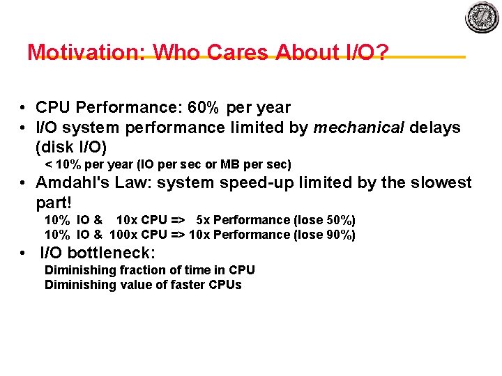
Motivation: Who Cares About I/O? • CPU Performance: 60% per year • I/O system performance limited by mechanical delays (disk I/O) < 10% per year (IO per sec or MB per sec) • Amdahl's Law: system speed up limited by the slowest part! 10% IO & 10 x CPU => 5 x Performance (lose 50%) 10% IO & 100 x CPU => 10 x Performance (lose 90%) • I/O bottleneck: Diminishing fraction of time in CPU Diminishing value of faster CPUs

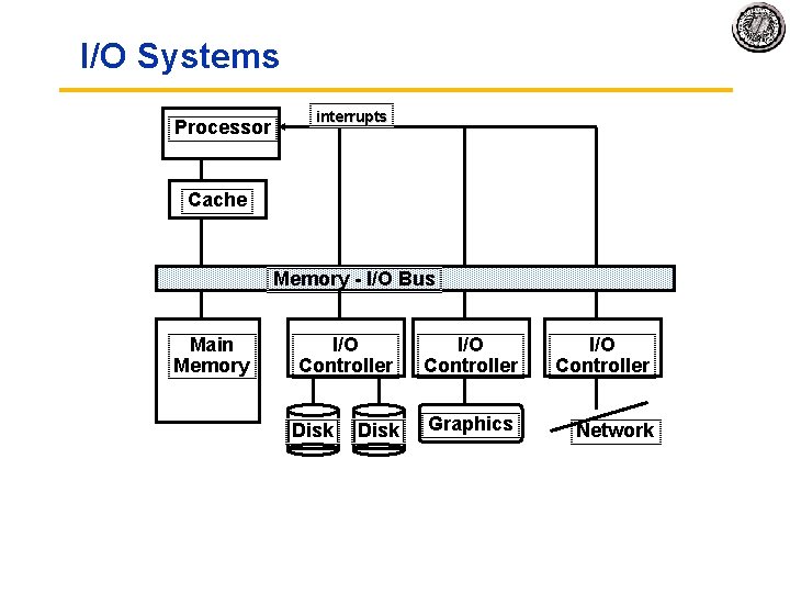
I/O Systems Processor interrupts Cache Memory I/O Bus Main Memory I/O Controller Disk I/O Controller Graphics Network

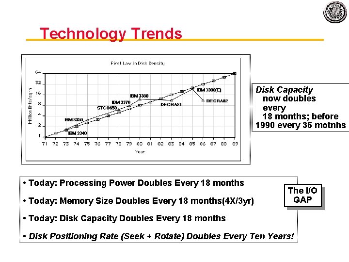
Technology Trends Disk Capacity now doubles every 18 months; before 1990 every 36 motnhs • Today: Processing Power Doubles Every 18 months • Today: Memory Size Doubles Every 18 months(4 X/3 yr) The I/O GAP • Today: Disk Capacity Doubles Every 18 months • Disk Positioning Rate (Seek + Rotate) Doubles Every Ten Years!

Storage Technology Drivers • Driven by the prevailing computing paradigm – 1950 s: migration from batch to on line processing – 1990 s: migration to ubiquitous computing » computers in phones, books, cars, video cameras, … » nationwide fiber optical network with wireless tails • Effects on storage industry: – Embedded storage » smaller, cheaper, more reliable, lower power – Data utilities » high capacity, hierarchically managed storage

Historical Perspective • 1956 IBM Ramac — early 1970 s Winchester – Developed for mainframe computers, proprietary interfaces – Steady shrink in form factor: 27 in. to 14 in. • 1970 s developments – 5. 25 inch floppy disk formfactor (microcode into mainframe) – early emergence of industry standard disk interfaces » ST 506, SASI, SMD, ESDI • Early 1980 s – PCs and first generation workstations • Mid 1980 s – Client/server computing – Centralized storage on file server » accelerates disk downsizing: 8 inch to 5. 25 inch – Mass market disk drives become a reality » industry standards: SCSI, IPI, IDE » 5. 25 inch drives for standalone PCs, End of proprietary interfaces

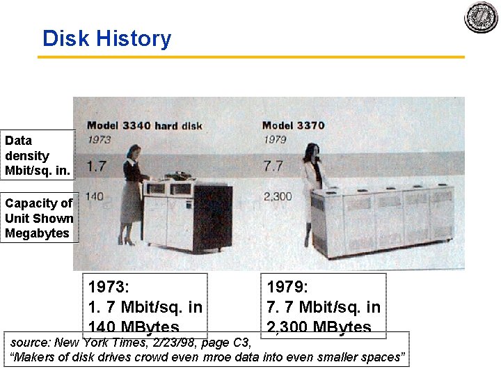
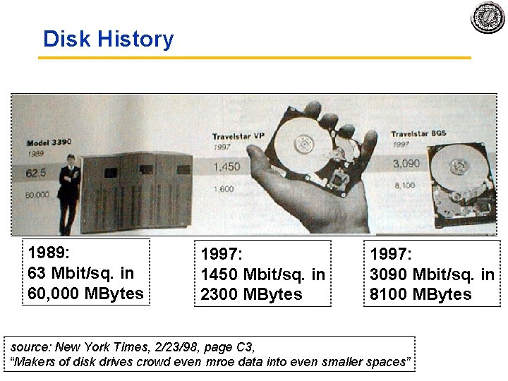
Disk History Data density Mbit/sq. in. Capacity of Unit Shown Megabytes 1973: 1. 7 Mbit/sq. in 140 MBytes 1979: 7. 7 Mbit/sq. in 2, 300 MBytes source: New York Times, 2/23/98, page C 3, “Makers of disk drives crowd even mroe data into even smaller spaces”

Historical Perspective • Late 1980 s/Early 1990 s: – Laptops, notebooks, (palmtops) – 3. 5 inch, 2. 5 inch, (1. 8 inch formfactors) – Formfactor plus capacity drives market, not so much performance » Recently Bandwidth improving at 40%/ year – Challenged by DRAM, flash RAM in PCMCIA cards » still expensive, Intel promises but doesn’t deliver » unattractive MBytes per cubic inch – Optical disk fails on performace (e. g. , NEXT) but finds niche (CD ROM)

Disk History 1989: 63 Mbit/sq. in 60, 000 MBytes 1997: 1450 Mbit/sq. in 2300 MBytes 1997: 3090 Mbit/sq. in 8100 MBytes source: New York Times, 2/23/98, page C 3, “Makers of disk drives crowd even mroe data into even smaller spaces”

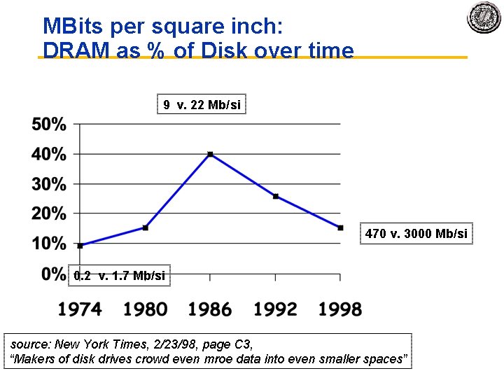
MBits per square inch: DRAM as % of Disk over time 9 v. 22 Mb/si 470 v. 3000 Mb/si 0. 2 v. 1. 7 Mb/si source: New York Times, 2/23/98, page C 3, “Makers of disk drives crowd even mroe data into even smaller spaces”

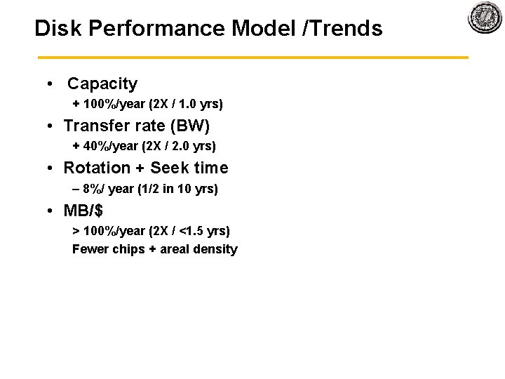
Disk Performance Model /Trends • Capacity + 100%/year (2 X / 1. 0 yrs) • Transfer rate (BW) + 40%/year (2 X / 2. 0 yrs) • Rotation + Seek time – 8%/ year (1/2 in 10 yrs) • MB/$ > 100%/year (2 X / <1. 5 yrs) Fewer chips + areal density

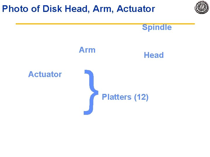
Photo of Disk Head, Arm, Actuator Spindle Arm { Actuator Head Platters (12)

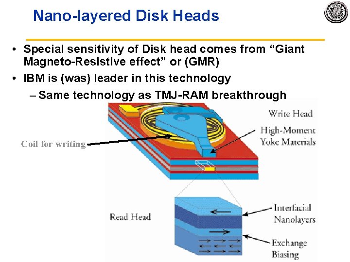
Nano layered Disk Heads • Special sensitivity of Disk head comes from “Giant Magneto Resistive effect” or (GMR) • IBM is (was) leader in this technology – Same technology as TMJ RAM breakthrough Coil for writing

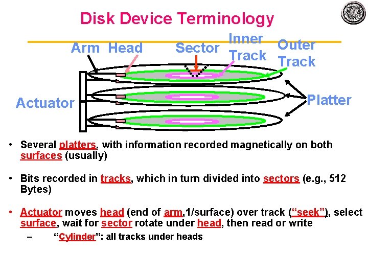
Disk Device Terminology Arm Head Inner Outer Sector Track Actuator Platter • Several platters, with information recorded magnetically on both surfaces (usually) • Bits recorded in tracks, which in turn divided into sectors (e. g. , 512 Bytes) • Actuator moves head (end of arm, 1/surface) over track (“seek”), select surface, wait for sector rotate under head, then read or write – “Cylinder”: all tracks under heads

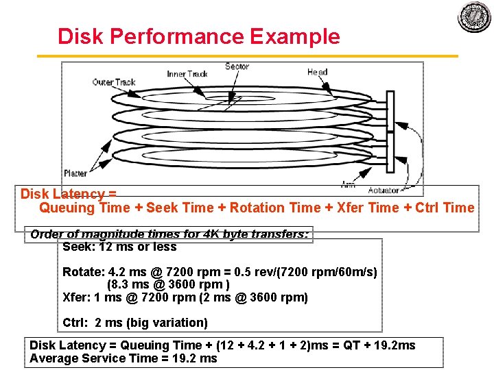
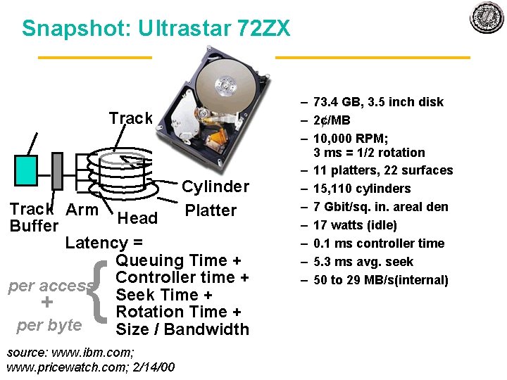
Disk Performance Example Disk Latency = Queuing Time + Seek Time + Rotation Time + Xfer Time + Ctrl Time Order of magnitude times for 4 K byte transfers: Seek: 12 ms or less Rotate: 4. 2 ms @ 7200 rpm = 0. 5 rev/(7200 rpm/60 m/s) (8. 3 ms @ 3600 rpm ) Xfer: 1 ms @ 7200 rpm (2 ms @ 3600 rpm) Ctrl: 2 ms (big variation) Disk Latency = Queuing Time + (12 + 4. 2 + 1 + 2)ms = QT + 19. 2 ms Average Service Time = 19. 2 ms

Disk Time Example • Disk Parameters: – – Transfer size is 8 K bytes Advertised average seek is 12 ms Disk spins at 7200 RPM Transfer rate is 4 MB/sec • Controller overhead is 2 ms • Assume that disk is idle so no queuing delay • What is Average Disk Access Time for a Sector? – Ave seek + ave rot delay + transfer time + controller overhead – 12 ms + 0. 5/(7200 RPM/60) + 8 KB/4 MB/s + 2 ms – 12 + 4. 15 + 2 = 20 ms • Advertised seek time assumes no locality: typically 1/4 to 1/3 advertised seek time: 20 ms => 12 ms

Snapshot: Ultrastar 72 ZX Track Sector Cylinder Track Arm Platter Head Buffer Latency = Queuing Time + Controller time + per access Seek Time + + Rotation Time + per byte Size / Bandwidth { source: www. ibm. com; www. pricewatch. com; 2/14/00 – 73. 4 GB, 3. 5 inch disk – 2¢/MB – 10, 000 RPM; 3 ms = 1/2 rotation – 11 platters, 22 surfaces – 15, 110 cylinders – 7 Gbit/sq. in. areal den – 17 watts (idle) – 0. 1 ms controller time – 5. 3 ms avg. seek – 50 to 29 MB/s(internal)

What Kind of Errors • • • In Memory In Disks? In networks? On Tapes? In distributed storage systems?

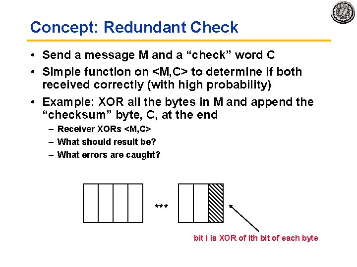
Concept: Redundant Check • Send a message M and a “check” word C • Simple function on <M, C> to determine if both received correctly (with high probability) • Example: XOR all the bytes in M and append the “checksum” byte, C, at the end – Receiver XORs <M, C> – What should result be? – What errors are caught? *** bit i is XOR of ith bit of each byte

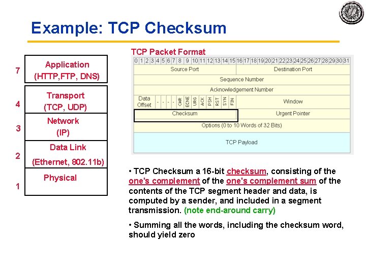
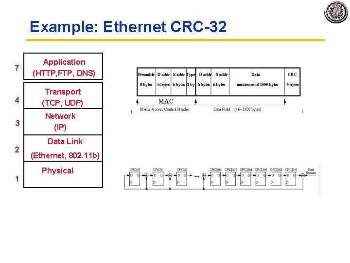
Example: TCP Checksum TCP Packet Format 7 Application (HTTP, FTP, DNS) 4 Transport (TCP, UDP) 3 2 1 Network (IP) Data Link (Ethernet, 802. 11 b) Physical • TCP Checksum a 16 bit checksum, consisting of the one's complement sum of the contents of the TCP segment header and data, is computed by a sender, and included in a segment transmission. (note end around carry) • Summing all the words, including the checksum word, should yield zero

Example: Ethernet CRC 32 7 Application (HTTP, FTP, DNS) 4 Transport (TCP, UDP) 3 2 1 Network (IP) Data Link (Ethernet, 802. 11 b) Physical

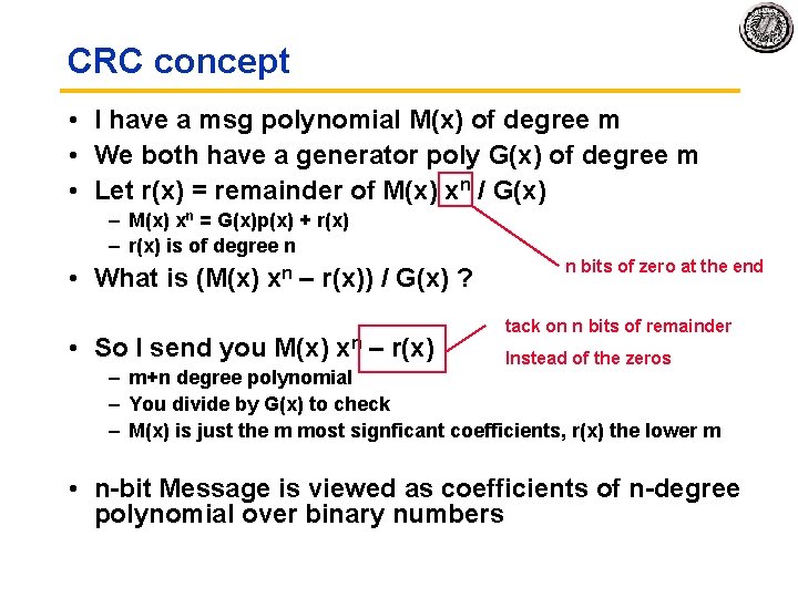
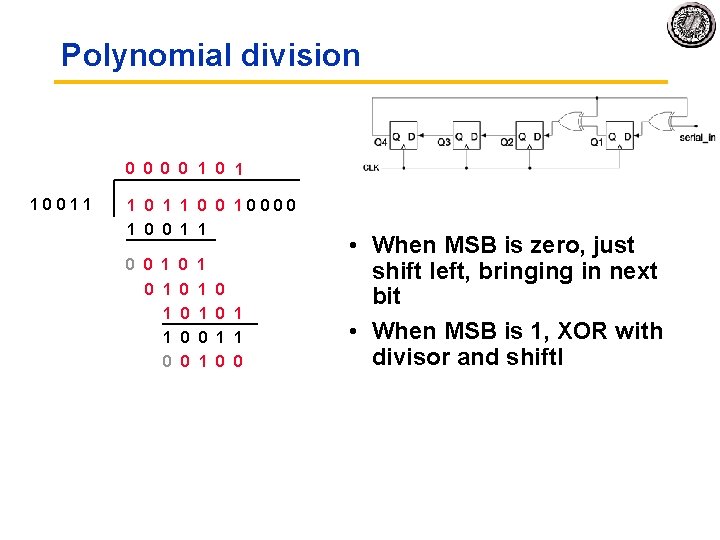
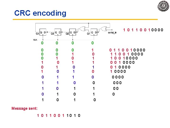
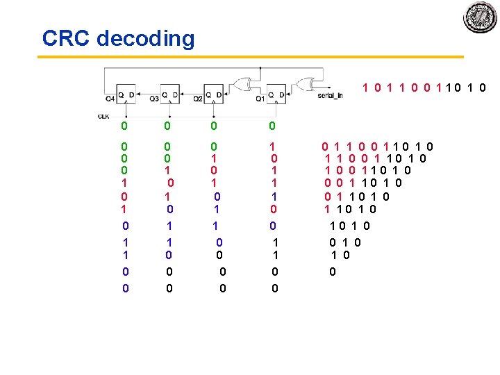
CRC concept • I have a msg polynomial M(x) of degree m • We both have a generator poly G(x) of degree m • Let r(x) = remainder of M(x) xn / G(x) – M(x) xn = G(x)p(x) + r(x) – r(x) is of degree n • What is (M(x) xn – r(x)) / G(x) ? • So I send you M(x) xn – r(x) n bits of zero at the end tack on n bits of remainder Instead of the zeros – m+n degree polynomial – You divide by G(x) to check – M(x) is just the m most signficant coefficients, r(x) the lower m • n bit Message is viewed as coefficients of n degree polynomial over binary numbers

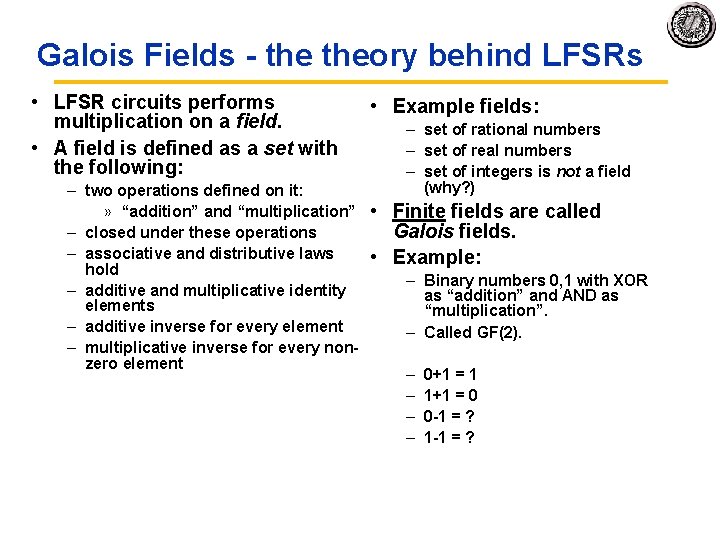
Galois Fields theory behind LFSRs • LFSR circuits performs multiplication on a field. • A field is defined as a set with the following: – two operations defined on it: » “addition” and “multiplication” – closed under these operations – associative and distributive laws hold – additive and multiplicative identity elements – additive inverse for every element – multiplicative inverse for every non zero element • Example fields: – set of rational numbers – set of real numbers – set of integers is not a field (why? ) • Finite fields are called Galois fields. • Example: – Binary numbers 0, 1 with XOR as “addition” and AND as “multiplication”. – Called GF(2). – – 0+1 = 1 1+1 = 0 0 1 = ? 1 1 = ?

Galois Fields The theory behind LFSRs • Consider polynomials whose coefficients come from GF(2). • Each term of the form xn is either present or absent. • Examples: 0, 1, x, x 2, and x 7 + x 6 + 1 = 1·x 7 + 1· x 6 + 0 · x 5 + 0 · x 4 + 0 · x 3 + 0 · x 2 + 0 · x 1 + 1· x 0 • With addition and multiplication these form a field: • “Add”: XOR each element individually with no carry: x 4 + x 3 + +x+1 + x 4 + + x 2 + x x 3 + x 2 +1 • “Multiply”: multiplying by xn is like shifting to the left. x 2 + x + 1 x+1 x 2 + x + 1 x 3 + x 2 + x x 3 +1

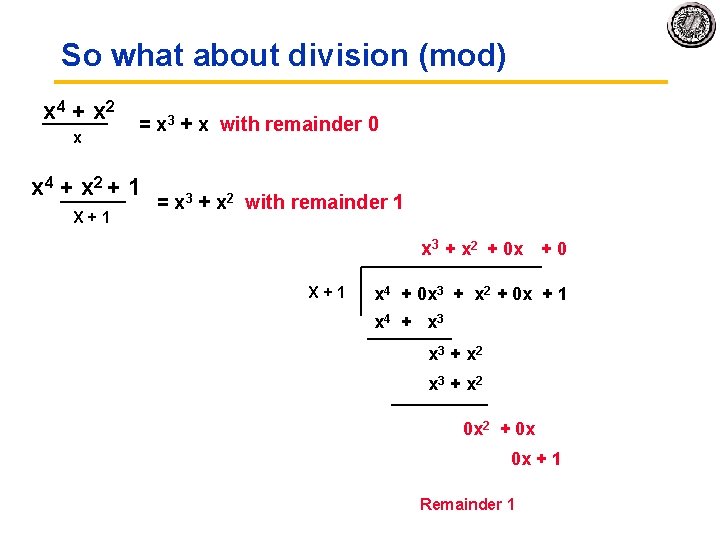
So what about division (mod) x 4 + x 2 = x 3 + x with remainder 0 x x 4 + x 2 + 1 X + 1 = x 3 + x 2 with remainder 1 x 3 + x 2 + 0 x + 0 X + 1 x 4 + 0 x 3 + x 2 + 0 x + 1 x 4 + x 3 + x 2 0 x 2 + 0 x 0 x + 1 Remainder 1

Polynomial division 0 0 1 0 1 1 0 0 1 0 0 1 0 1 0 1 0 1 1 0 0 • When MSB is zero, just shift left, bringing in next bit • When MSB is 1, XOR with divisor and shiftl

CRC encoding 1 0 1 1 0 0 0 0 0 0 0 1 0 1 1 0 0 0 0 0 0 1 0 1 1 0 0 0 0 0 1 1 0 0 0 0 1 0 1 1 0 0 1 0 0 0 1 0 1 0 0 1 0 1 0 1 0 0 1 0 0 0 1 1 0 0 0 0 1 0 1 0 0 1 0 1 0 1 0 Message sent: 1 0 1 0

CRC decoding 1 0 1 0 0 0 0 1 0 1 1 0 1 0 0 0 1 0 1 1 0 1 0 0 1 1 0 0 1 1 0 1 0 1 1 0 0 1 1 0 0 1 0 1 1 0 1 0 1 0 1 1 0 1 0 1 0 1 1 0 1 0 1 0 0 0

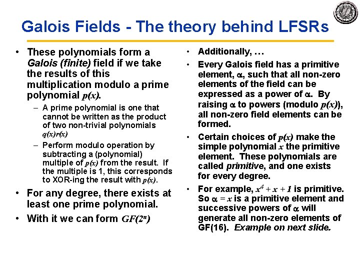
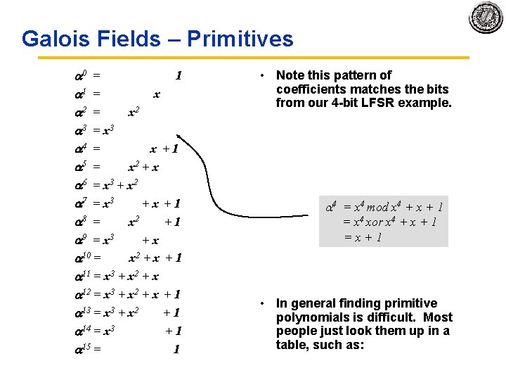
Galois Fields The theory behind LFSRs • These polynomials form a Galois (finite) field if we take the results of this multiplication modulo a prime polynomial p(x). – A prime polynomial is one that cannot be written as the product of two non trivial polynomials q(x)r(x) – Perform modulo operation by subtracting a (polynomial) multiple of p(x) from the result. If the multiple is 1, this corresponds to XOR ing the result with p(x). • For any degree, there exists at least one prime polynomial. • With it we can form GF(2 n) • Additionally, … • Every Galois field has a primitive element, , such that all non zero elements of the field can be expressed as a power of . By raising to powers (modulo p(x)), all non zero field elements can be formed. • Certain choices of p(x) make the simple polynomial x the primitive element. These polynomials are called primitive, and one exists for every degree. • For example, x 4 + x + 1 is primitive. So = x is a primitive element and successive powers of will generate all non zero elements of GF(16). Example on next slide.

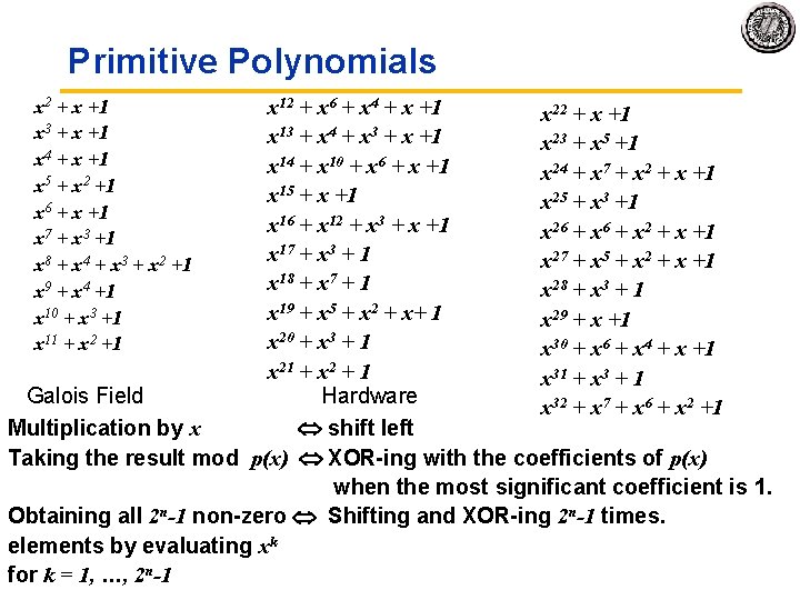
Galois Fields – Primitives 0 = 1 1 = x 2 3 = x 3 4 = x +1 5 = x 2 + x 6 = x 3 + x 2 7 = x 3 +x +1 8 = x 2 +1 9 = x 3 +x 10 = x 2 + x + 1 11 = x 3 + x 2 + x 12 = x 3 + x 2 + x + 1 13 = x 3 + x 2 +1 14 = x 3 +1 15 = 1 • Note this pattern of coefficients matches the bits from our 4 bit LFSR example. 4 = x 4 mod x 4 + x + 1 = x 4 xor x 4 + x + 1 =x+1 • In general finding primitive polynomials is difficult. Most people just look them up in a table, such as:

Primitive Polynomials x 12 + x 6 + x 4 + x +1 x 22 + x +1 x 13 + x 4 + x 3 + x +1 x 23 + x 5 +1 x 14 + x 10 + x 6 + x +1 x 24 + x 7 + x 2 + x +1 x 15 + x +1 x 25 + x 3 +1 x 16 + x 12 + x 3 + x +1 x 26 + x 2 + x +1 x 17 + x 3 + 1 x 27 + x 5 + x 2 + x +1 x 18 + x 7 + 1 x 28 + x 3 + 1 x 19 + x 5 + x 2 + x+ 1 x 29 + x +1 x 20 + x 3 + 1 x 30 + x 6 + x 4 + x +1 x 21 + x 2 + 1 x 31 + x 3 + 1 Galois Field Hardware x 32 + x 7 + x 6 + x 2 +1 Multiplication by x shift left Taking the result mod p(x) XOR ing with the coefficients of p(x) when the most significant coefficient is 1. Obtaining all 2 n-1 non zero Shifting and XOR ing 2 n-1 times. elements by evaluating xk for k = 1, …, 2 n-1 x 2 + x +1 x 3 + x +1 x 4 + x +1 x 5 + x 2 +1 x 6 + x +1 x 7 + x 3 +1 x 8 + x 4 + x 3 + x 2 +1 x 9 + x 4 +1 x 10 + x 3 +1 x 11 + x 2 +1

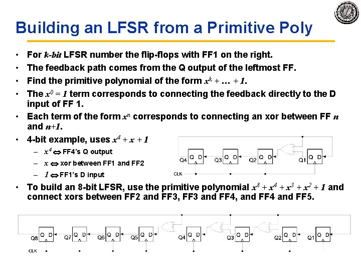
Building an LFSR from a Primitive Poly • • For k-bit LFSR number the flip flops with FF 1 on the right. The feedback path comes from the Q output of the leftmost FF. Find the primitive polynomial of the form xk + … + 1. The x 0 = 1 term corresponds to connecting the feedback directly to the D input of FF 1. • Each term of the form xn corresponds to connecting an xor between FF n and n+1. • 4 bit example, uses x 4 + x + 1 – x 4 FF 4’s Q output – x xor between FF 1 and FF 2 – 1 FF 1’s D input • To build an 8 bit LFSR, use the primitive polynomial x 8 + x 4 + x 3 + x 2 + 1 and connect xors between FF 2 and FF 3, FF 3 and FF 4, and FF 4 and FF 5.

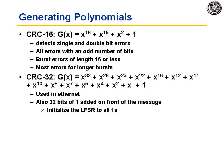
Generating Polynomials • CRC 16: G(x) = x 16 + x 15 + x 2 + 1 – – detects single and double bit errors All errors with an odd number of bits Burst errors of length 16 or less Most errors for longer bursts • CRC 32: G(x) = x 32 + x 26 + x 23 + x 22 + x 16 + x 12 + x 11 + x 10 + x 8 + x 7 + x 5 + x 4 + x 2 + x + 1 – Used in ethernet – Also 32 bits of 1 added on front of the message » Initialize the LFSR to all 1 s

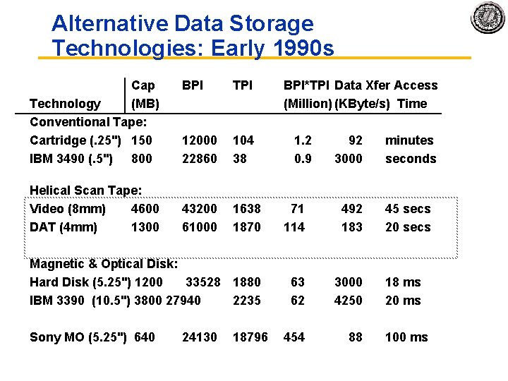
Alternative Data Storage Technologies: Early 1990 s Cap Technology (MB) Conventional Tape: Cartridge (. 25") 150 IBM 3490 (. 5") 800 BPI TPI BPI*TPI Data Xfer Access (Million) (KByte/s) Time 12000 22860 104 38 1. 2 0. 9 92 3000 minutes seconds 43200 61000 1638 1870 71 114 492 183 45 secs 20 secs Magnetic & Optical Disk: Hard Disk (5. 25") 1200 33528 1880 IBM 3390 (10. 5") 3800 27940 2235 63 62 3000 4250 18 ms 20 ms Sony MO (5. 25") 640 454 88 100 ms Helical Scan Tape: Video (8 mm) 4600 DAT (4 mm) 1300 24130 18796

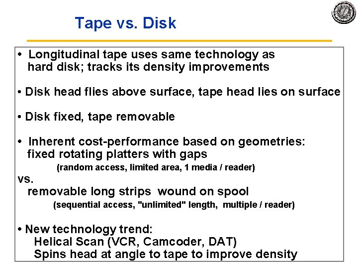
Tape vs. Disk • Longitudinal tape uses same technology as hard disk; tracks its density improvements • Disk head flies above surface, tape head lies on surface • Disk fixed, tape removable • Inherent cost performance based on geometries: fixed rotating platters with gaps (random access, limited area, 1 media / reader) vs. removable long strips wound on spool (sequential access, "unlimited" length, multiple / reader) • New technology trend: Helical Scan (VCR, Camcoder, DAT) Spins head at angle to tape to improve density

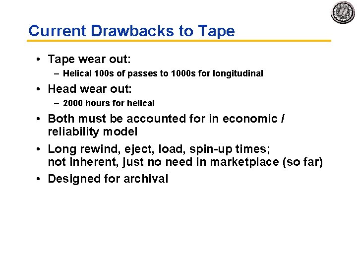
Current Drawbacks to Tape • Tape wear out: – Helical 100 s of passes to 1000 s for longitudinal • Head wear out: – 2000 hours for helical • Both must be accounted for in economic / reliability model • Long rewind, eject, load, spin up times; not inherent, just no need in marketplace (so far) • Designed for archival

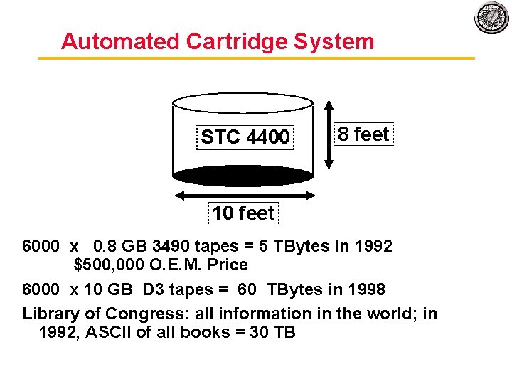
Automated Cartridge System STC 4400 8 feet 10 feet 6000 x 0. 8 GB 3490 tapes = 5 TBytes in 1992 $500, 000 O. E. M. Price 6000 x 10 GB D 3 tapes = 60 TBytes in 1998 Library of Congress: all information in the world; in 1992, ASCII of all books = 30 TB

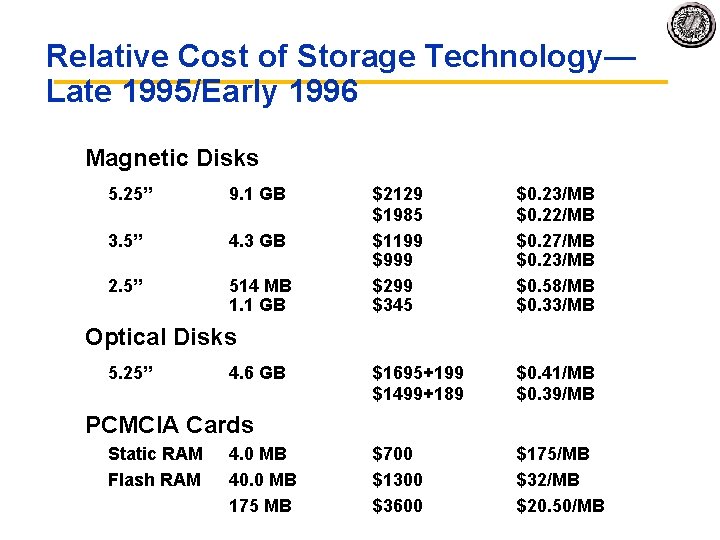
Relative Cost of Storage Technology— Late 1995/Early 1996 Magnetic Disks 5. 25” 9. 1 GB 3. 5” 4. 3 GB 2. 5” 514 MB 1. 1 GB $2129 $1985 $1199 $999 $299 $345 $0. 23/MB $0. 22/MB $0. 27/MB $0. 23/MB $0. 58/MB $0. 33/MB $1695+199 $1499+189 $0. 41/MB $0. 39/MB $700 $1300 $3600 $175/MB $32/MB $20. 50/MB Optical Disks 5. 25” 4. 6 GB PCMCIA Cards Static RAM Flash RAM 4. 0 MB 40. 0 MB 175 MB

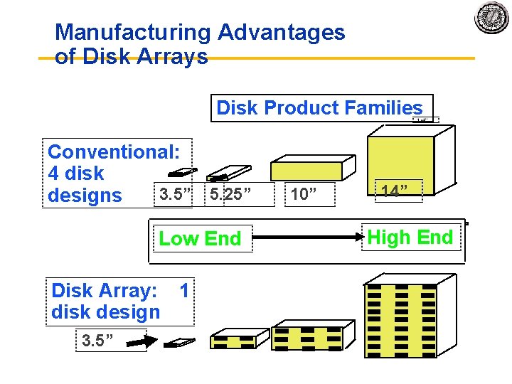
Manufacturing Advantages of Disk Arrays Disk Product Families Conventional: 4 disk 3. 5” 5. 25” 10” designs Low End Disk Array: 1 disk design 3. 5” 14” High End

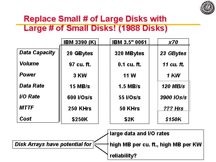
Replace Small # of Large Disks with Large # of Small Disks! (1988 Disks) IBM 3390 (K) IBM 3. 5" 0061 x 70 20 GBytes 320 MBytes 23 GBytes 97 cu. ft. 0. 1 cu. ft. 11 cu. ft. 3 KW 11 W 1 KW Data Rate 15 MB/s 120 MB/s I/O Rate 600 I/Os/s 55 I/Os/s 3900 IOs/s MTTF 250 KHrs ? ? ? Hrs Cost $250 K $2 K $150 K Data Capacity Volume Power large data and I/O rates Disk Arrays have potential for high MB per cu. ft. , high MB per KW reliability?

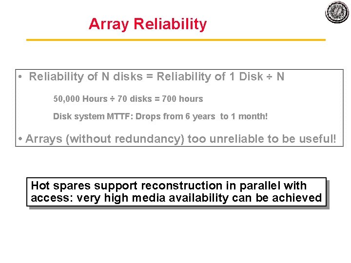
Array Reliability • Reliability of N disks = Reliability of 1 Disk ÷ N 50, 000 Hours ÷ 70 disks = 700 hours Disk system MTTF: Drops from 6 years to 1 month! • Arrays (without redundancy) too unreliable to be useful! Hot spares support reconstruction in parallel with access: very high media availability can be achieved

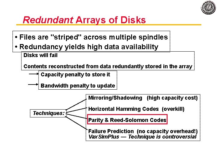
Redundant Arrays of Disks • Files are "striped" across multiple spindles • Redundancy yields high data availability Disks will fail Contents reconstructed from data redundantly stored in the array Capacity penalty to store it Bandwidth penalty to update Mirroring/Shadowing (high capacity cost) Techniques: Horizontal Hamming Codes (overkill) Parity & Reed Solomon Codes Failure Prediction (no capacity overhead!) Vax. Sim. Plus — Technique is controversial

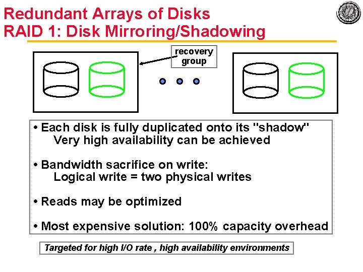
Redundant Arrays of Disks RAID 1: Disk Mirroring/Shadowing recovery group • Each disk is fully duplicated onto its "shadow" Very high availability can be achieved • Bandwidth sacrifice on write: Logical write = two physical writes • Reads may be optimized • Most expensive solution: 100% capacity overhead Targeted for high I/O rate , high availability environments

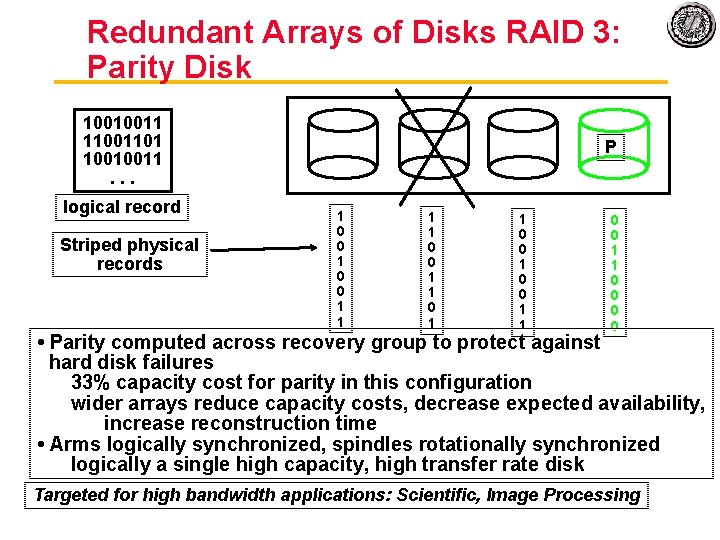
Redundant Arrays of Disks RAID 3: Parity Disk 10010011 11001101 10010011. . . logical record Striped physical records P 1 0 0 1 1 0 0 1 1 0 0 • Parity computed across recovery group to protect against hard disk failures 33% capacity cost for parity in this configuration wider arrays reduce capacity costs, decrease expected availability, increase reconstruction time • Arms logically synchronized, spindles rotationally synchronized logically a single high capacity, high transfer rate disk Targeted for high bandwidth applications: Scientific, Image Processing

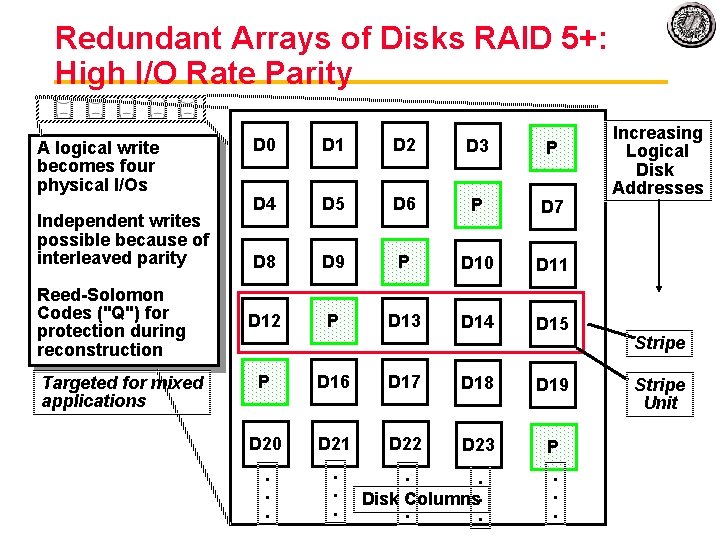
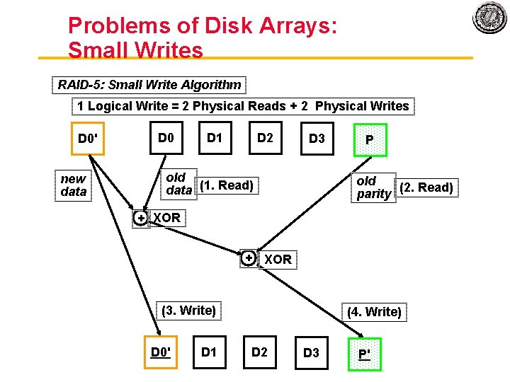
Redundant Arrays of Disks RAID 5+: High I/O Rate Parity A logical write becomes four physical I/Os Independent writes possible because of interleaved parity Reed Solomon Codes ("Q") for protection during reconstruction Targeted for mixed applications D 0 D 1 D 2 D 3 P D 4 D 5 D 6 P D 7 D 8 D 9 P D 10 D 11 D 12 P D 13 D 14 D 15 P D 16 D 17 D 18 D 19 D 20 D 21 D 22 D 23 P . . Disk Columns. . . Increasing Logical Disk Addresses Stripe Unit

Problems of Disk Arrays: Small Writes RAID-5: Small Write Algorithm 1 Logical Write = 2 Physical Reads + 2 Physical Writes D 0' new data D 0 D 1 D 2 D 3 old data (1. Read) P old (2. Read) parity + XOR (3. Write) D 0' D 1 (4. Write) D 2 D 3 P'

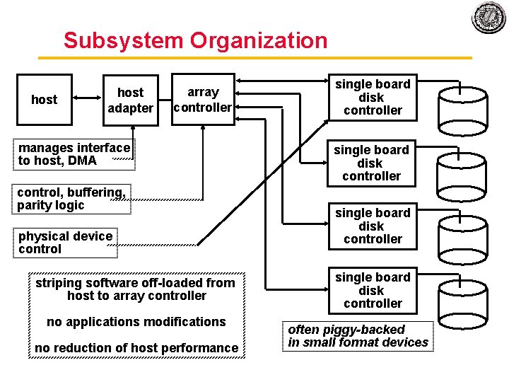
Subsystem Organization host adapter array controller manages interface to host, DMA control, buffering, parity logic physical device control striping software off loaded from host to array controller no applications modifications no reduction of host performance single board disk controller often piggy-backed in small format devices

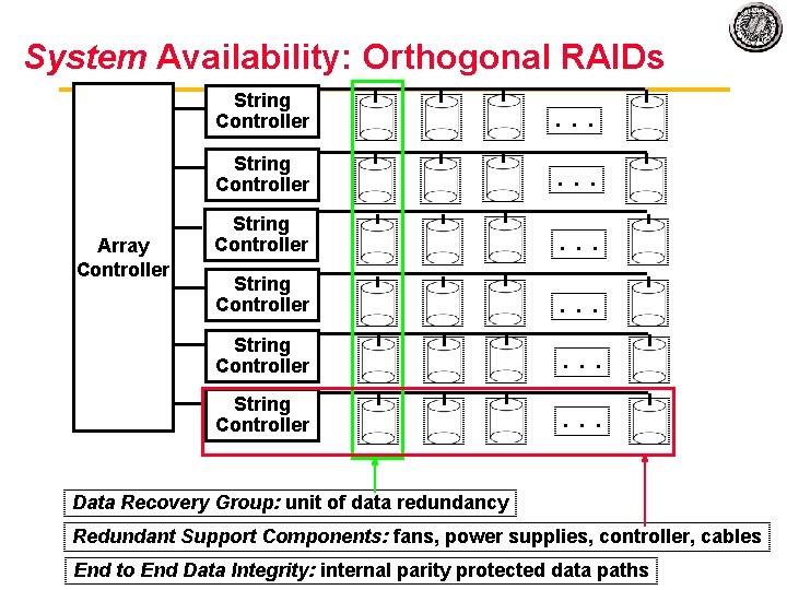
System Availability: Orthogonal RAIDs Array Controller String Controller . . . Data Recovery Group: unit of data redundancy Redundant Support Components: fans, power supplies, controller, cables End to End Data Integrity: internal parity protected data paths

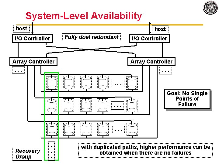
System Level Availability host Fully dual redundant I/O Controller Array Controller . . . Goal: No Single Points of Failure . . . Recovery Group . . . with duplicated paths, higher performance can be obtained when there are no failures

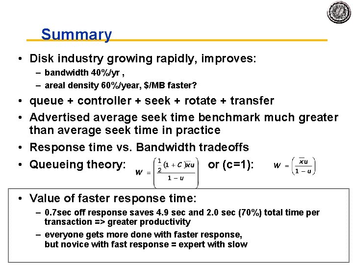
Summary • Disk industry growing rapidly, improves: – bandwidth 40%/yr , – areal density 60%/year, $/MB faster? • queue + controller + seek + rotate + transfer • Advertised average seek time benchmark much greater than average seek time in practice • Response time vs. Bandwidth tradeoffs • Queueing theory: or (c=1): • Value of faster response time: – 0. 7 sec off response saves 4. 9 sec and 2. 0 sec (70%) total time per transaction => greater productivity – everyone gets more done with faster response, but novice with fast response = expert with slow