EECS 150 Components and Design Techniques for Digital


- Slides: 49

EECS 150 - Components and Design Techniques for Digital Systems Lec 02 – Gates and CMOS Technology 8 -30 -07 David Culler Electrical Engineering and Computer Sciences University of California, Berkeley http: //www. eecs. berkeley. edu/~culler http: //inst. eecs. berkeley. edu/~cs 150 8/30/2007 © UC Berkeley EECS 150 -F 05 CMOS lec 02 1

Outline • • Summary of last time Overview of Physical Implementations Boolean Logic CMOS devices Combinational Logic Announcements/Break CMOS transistor circuits – basic logic gates – tri-state buffers – flip-flops » flip-flop timing basics » example use » circuits 8/30/2007 © UC Berkeley EECS 150 -F 05 CMOS lec 02 2

L 01 Summary: Digital Design Given a functional description and performance, cost, & power constraints, come up with an implementation using a set of primitives. • How do we learn how to do this? 1. Learn about the primitives and how to generate them. 2. Learn about design representation. 3. Learn formal methods to optimally manipulate the representations. 4. Look at design examples. 5. Use trial and error - CAD tools and prototyping. • Digital design is in some ways more an art than a science. The creative spirit is critical in combining primitive elements & other components in new ways to achieve a desired function. • However, unlike art, we have objective measures of a design: performance cost power & Time to Market 8/30/2007 © UC Berkeley EECS 150 -F 05 CMOS lec 02 3

The Boolean Abstraction 8/30/2007 © UC Berkeley EECS 150 -F 05 CMOS lec 02 4

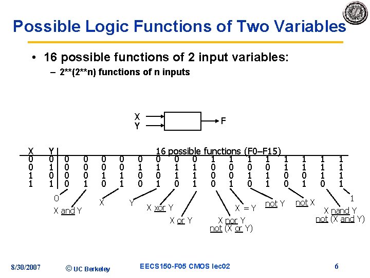
Possible Logic Functions of Two Variables • 16 possible functions of 2 input variables: – 2**(2**n) functions of n inputs X Y X 0 0 1 1 Y 0 1 0 0 0 X and Y 8/30/2007 0 0 0 1 0 X © UC Berkeley 0 0 1 1 F 0 1 0 0 Y 16 0 1 possible functions (F 0–F 15) 0 0 1 1 1 1 0 0 1 0 1 0 X xor Y X=Y X nor Y not (X or Y) EECS 150 -F 05 CMOS lec 02 not Y 1 1 0 1 not X 1 1 1 0 1 1 1 X nand Y not (X and Y) 6

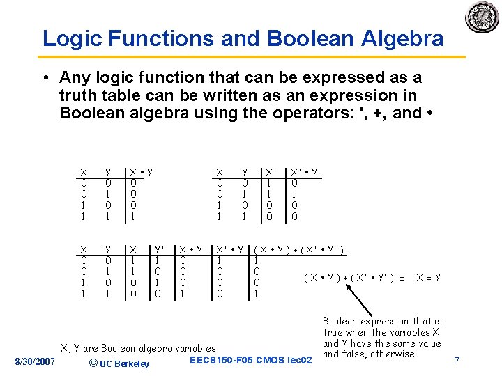
Logic Functions and Boolean Algebra • Any logic function that can be expressed as a truth table can be written as an expression in Boolean algebra using the operators: ', +, and • X 0 0 1 1 Y 0 1 X • Y 0 0 0 1 X 0 0 1 1 Y 0 1 X' 1 1 0 0 X 0 0 1 1 Y' 1 0 X • Y 0 0 0 1 Y 0 1 X' • Y' 1 0 0 0 X' 1 1 0 0 X' • Y 0 1 0 0 ( X • Y ) + ( X' • Y' ) 1 0 ( X • Y ) + ( X' • Y' ) 0 1 X, Y are Boolean algebra variables EECS 150 -F 05 CMOS lec 02 8/30/2007 © UC Berkeley X = Y Boolean expression that is true when the variables X and Y have the same value and false, otherwise 7

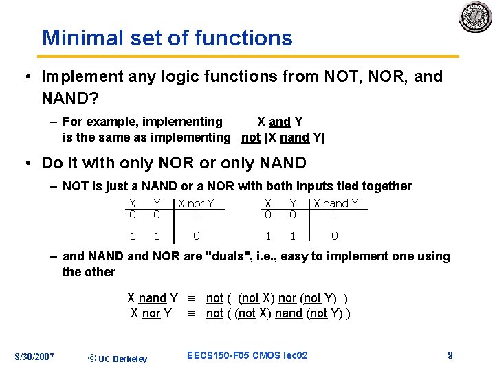
Minimal set of functions • Implement any logic functions from NOT, NOR, and NAND? – For example, implementing X and Y is the same as implementing not (X nand Y) • Do it with only NOR or only NAND – NOT is just a NAND or a NOR with both inputs tied together X 0 Y 0 X nor Y 1 X 0 Y 0 X nand Y 1 1 1 0 – and NAND and NOR are "duals", i. e. , easy to implement one using the other X nand Y not ( (not X) nor (not Y) ) X nor Y not ( (not X) nand (not Y) ) 8/30/2007 © UC Berkeley EECS 150 -F 05 CMOS lec 02 8

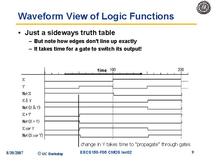
Waveform View of Logic Functions • Just a sideways truth table – But note how edges don't line up exactly – It takes time for a gate to switch its output! time change in Y takes time to "propagate" through gates 8/30/2007 © UC Berkeley EECS 150 -F 05 CMOS lec 02 9

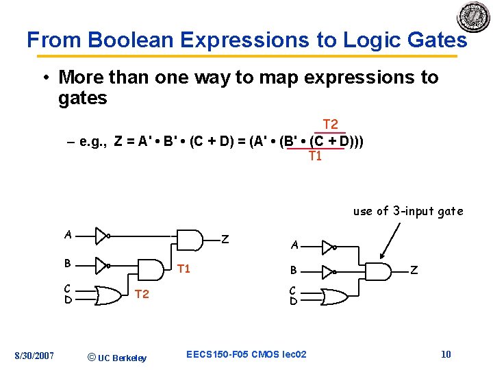
From Boolean Expressions to Logic Gates • More than one way to map expressions to gates T 2 – e. g. , Z = A' • B' • (C + D) = (A' • (B' • (C + D))) T 1 use of 3 -input gate A Z B C D 8/30/2007 T 1 T 2 © UC Berkeley A B Z C D EECS 150 -F 05 CMOS lec 02 10

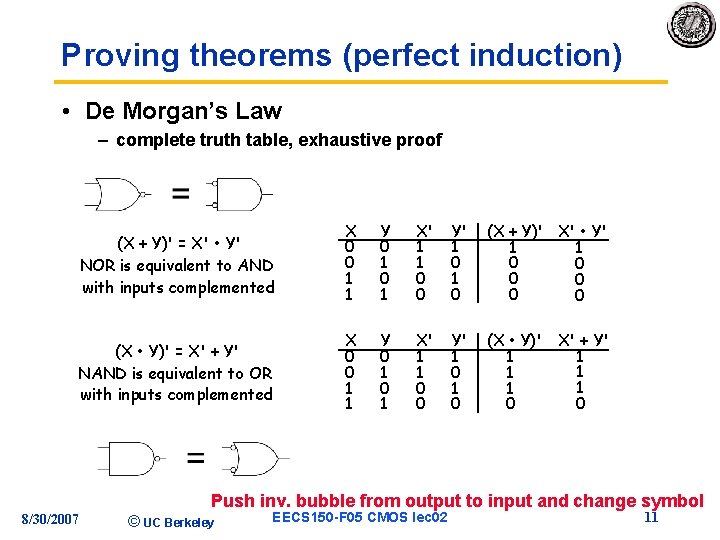
Proving theorems (perfect induction) • De Morgan’s Law – complete truth table, exhaustive proof (X + Y)' = X' • Y' NOR is equivalent to AND with inputs complemented X 0 0 1 1 Y 0 1 X' 1 1 0 0 Y' 1 0 (X + Y)' X' • Y' 1 1 0 0 0 (X • Y)' = X' + Y' NAND is equivalent to OR with inputs complemented X 0 0 1 1 Y 0 1 X' 1 1 0 0 Y' 1 0 (X • Y)' X' + Y' 1 1 1 0 0 Push inv. bubble from output to input and change symbol 8/30/2007 © UC Berkeley EECS 150 -F 05 CMOS lec 02 11

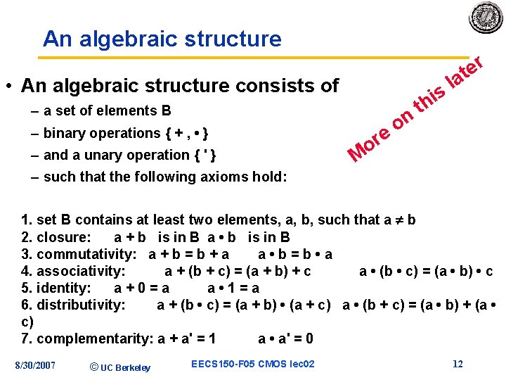
An algebraic structure • An algebraic structure consists of – a set of elements B e r o – binary operations { + , • } – and a unary operation { ' } on s i h la r e t t M – such that the following axioms hold: 1. set B contains at least two elements, a, b, such that a b 2. closure: a + b is in B a • b is in B 3. commutativity: a + b = b + a a • b=b • a 4. associativity: a + (b + c) = (a + b) + c a • (b • c) = (a • b) • c 5. identity: a+0=a a • 1=a 6. distributivity: a + (b • c) = (a + b) • (a + c) a • (b + c) = (a • b) + (a • c) 7. complementarity: a + a' = 1 a • a' = 0 8/30/2007 © UC Berkeley EECS 150 -F 05 CMOS lec 02 12

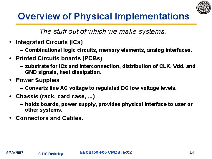
Overview of Physical Implementations The stuff out of which we make systems. • Integrated Circuits (ICs) – Combinational logic circuits, memory elements, analog interfaces. • Printed Circuits boards (PCBs) – substrate for ICs and interconnection, distribution of CLK, Vdd, and GND signals, heat dissipation. • Power Supplies – Converts line AC voltage to regulated DC low voltage levels. • Chassis (rack, card case, . . . ) – holds boards, power supply, provides physical interface to user or other systems. • Connectors and Cables. 8/30/2007 © UC Berkeley EECS 150 -F 05 CMOS lec 02 14

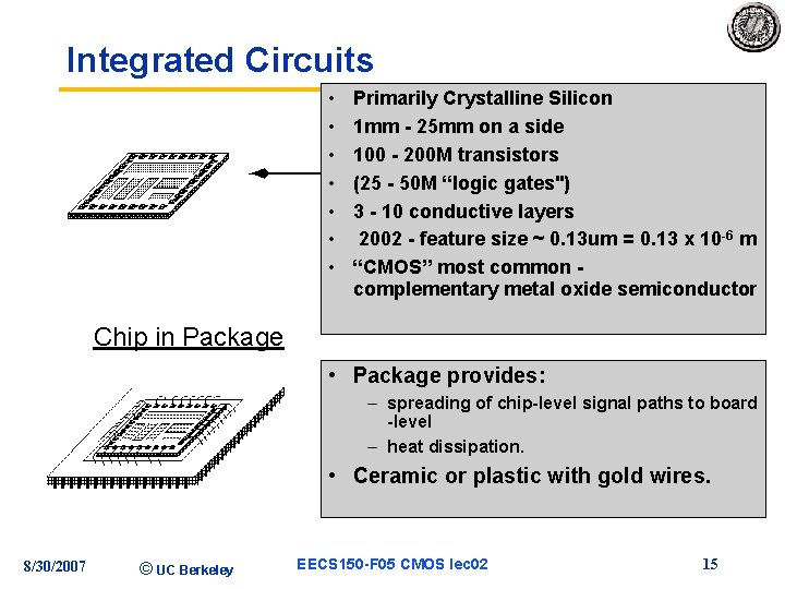
Integrated Circuits • • Primarily Crystalline Silicon 1 mm - 25 mm on a side 100 - 200 M transistors (25 - 50 M “logic gates") 3 - 10 conductive layers 2002 - feature size ~ 0. 13 um = 0. 13 x 10 -6 m “CMOS” most common complementary metal oxide semiconductor Chip in Package • Package provides: – spreading of chip-level signal paths to board -level – heat dissipation. • Ceramic or plastic with gold wires. 8/30/2007 © UC Berkeley EECS 150 -F 05 CMOS lec 02 15

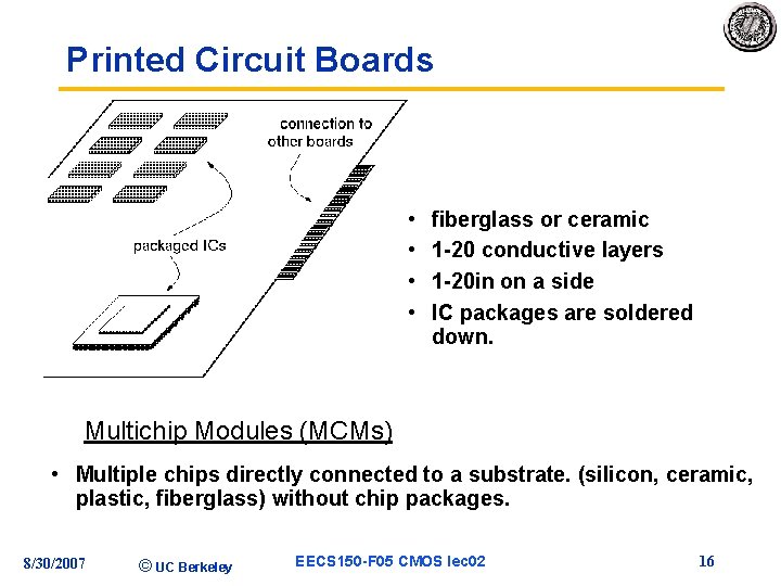
Printed Circuit Boards • • fiberglass or ceramic 1 -20 conductive layers 1 -20 in on a side IC packages are soldered down. Multichip Modules (MCMs) • Multiple chips directly connected to a substrate. (silicon, ceramic, plastic, fiberglass) without chip packages. 8/30/2007 © UC Berkeley EECS 150 -F 05 CMOS lec 02 16

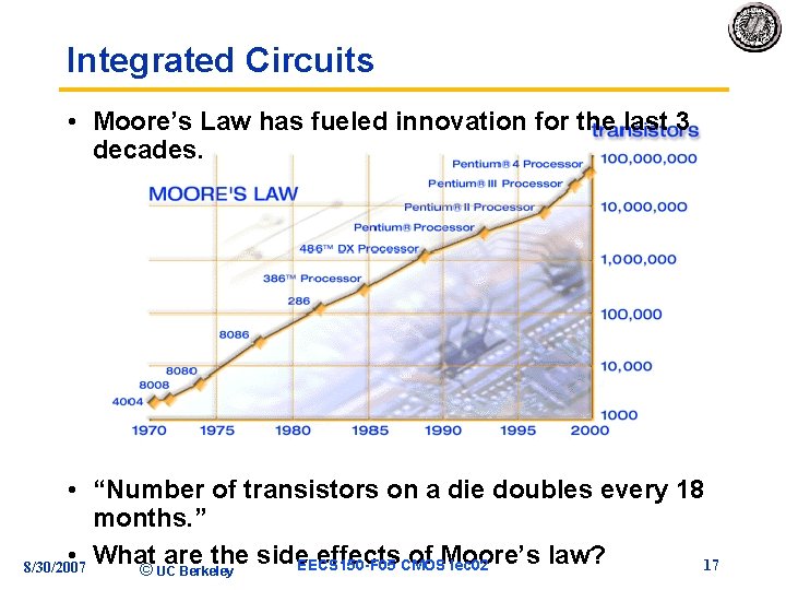
Integrated Circuits • Moore’s Law has fueled innovation for the last 3 decades. • “Number of transistors on a die doubles every 18 months. ” • What are the side. EECS 150 -F 05 effects. CMOS of Moore’s law? 17 lec 02 8/30/2007 © UC Berkeley

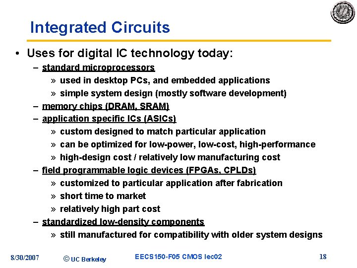
Integrated Circuits • Uses for digital IC technology today: – standard microprocessors » used in desktop PCs, and embedded applications » simple system design (mostly software development) – memory chips (DRAM, SRAM) – application specific ICs (ASICs) » custom designed to match particular application » can be optimized for low-power, low-cost, high-performance » high-design cost / relatively low manufacturing cost – field programmable logic devices (FPGAs, CPLDs) » customized to particular application after fabrication » short time to market » relatively high part cost – standardized low-density components » still manufactured for compatibility with older system designs 8/30/2007 © UC Berkeley EECS 150 -F 05 CMOS lec 02 18

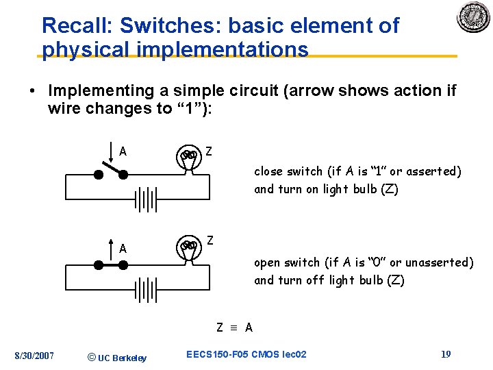
Recall: Switches: basic element of physical implementations • Implementing a simple circuit (arrow shows action if wire changes to “ 1”): A Z close switch (if A is “ 1” or asserted) and turn on light bulb (Z) A Z open switch (if A is “ 0” or unasserted) and turn off light bulb (Z) Z A 8/30/2007 © UC Berkeley EECS 150 -F 05 CMOS lec 02 19

CMOS Devices • MOSFET (Metal Oxide Semiconductor Field Effect Transistor). Top View Cross Section n. FET The gate acts like a capacitor. A high voltage on the gate attracts charge into the channel. If a voltage exists between the source and drain a current will flow. In its simplest approximation the device acts like a switch. 8/30/2007 © UC Berkeley EECS 150 -F 05 CMOS lec 02 p. FET 20

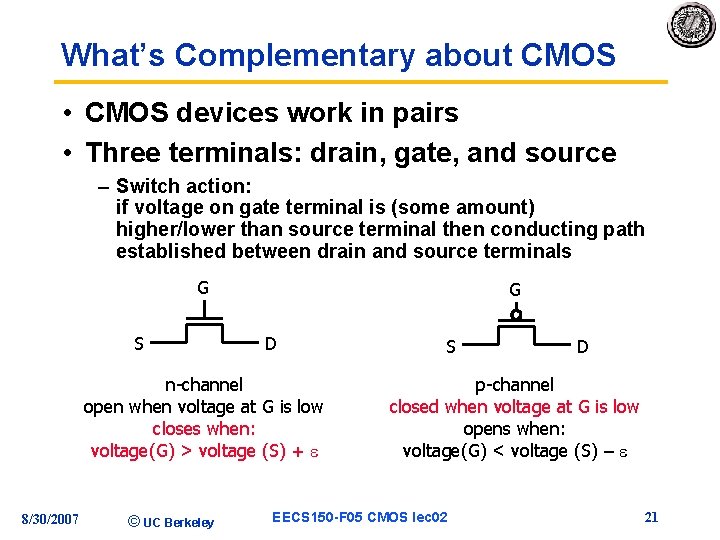
What’s Complementary about CMOS • CMOS devices work in pairs • Three terminals: drain, gate, and source – Switch action: if voltage on gate terminal is (some amount) higher/lower than source terminal then conducting path established between drain and source terminals G S G D n-channel open when voltage at G is low closes when: voltage(G) > voltage (S) + 8/30/2007 © UC Berkeley S D p-channel closed when voltage at G is low opens when: voltage(G) < voltage (S) – EECS 150 -F 05 CMOS lec 02 21

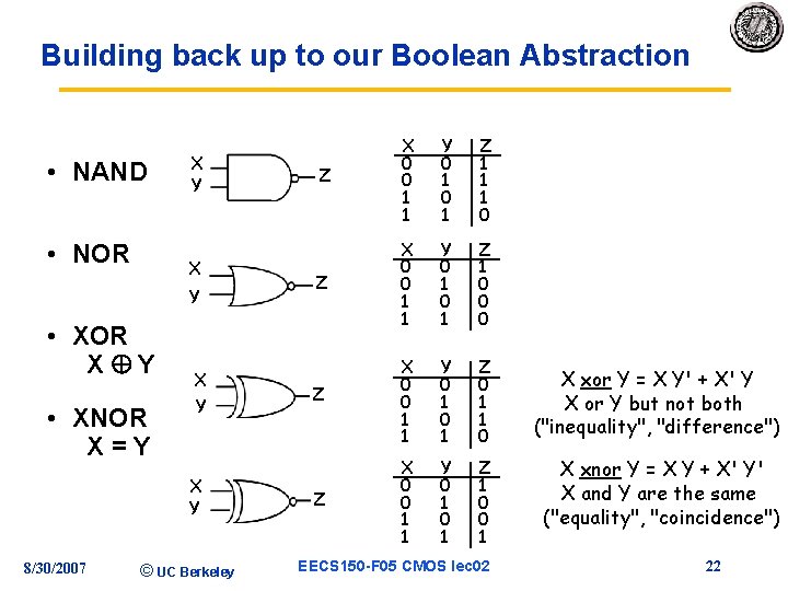
Building back up to our Boolean Abstraction • NAND • NOR X Y • XOR X Y • XNOR X=Y X Y 8/30/2007 © UC Berkeley Z X 0 0 1 1 Y 0 1 Z 1 1 1 0 Z X 0 0 1 1 Y 0 1 Z 1 0 0 0 Z X 0 0 1 1 Y 0 1 Z 0 1 1 0 Z X 0 0 1 1 Y 0 1 Z 1 0 0 1 EECS 150 -F 05 CMOS lec 02 X xor Y = X Y' + X' Y X or Y but not both ("inequality", "difference") X xnor Y = X Y + X' Y' X and Y are the same ("equality", "coincidence") 22

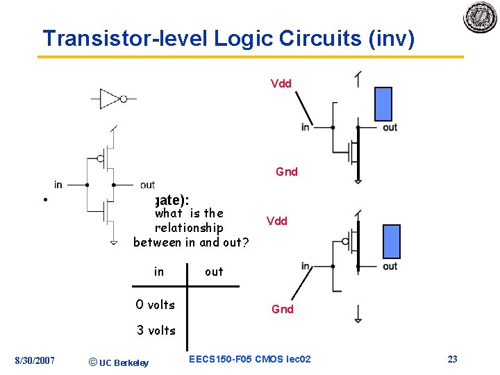
Transistor-level Logic Circuits (inv) Vdd Gnd • Inverter (NOT gate): what is the relationship between in and out? in 0 volts Vdd out Gnd 3 volts 8/30/2007 © UC Berkeley EECS 150 -F 05 CMOS lec 02 23

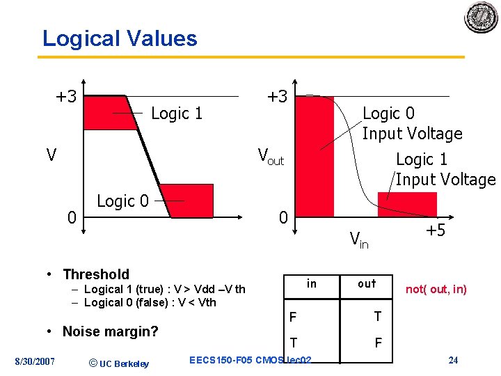
Logical Values +3 Logic 1 V +3 Logic 0 Input Voltage Vout 0 Logic 1 Input Voltage 0 +5 Vin • Threshold – Logical 1 (true) : V > Vdd –V th – Logical 0 (false) : V < Vth • Noise margin? 8/30/2007 © UC Berkeley in out F T T F EECS 150 -F 05 CMOS lec 02 not( out, in) 24

Big idea: Self-restoring logic • CMOS logic gates are self-restoring – Even if the inputs are imperfect, switching time is fast and outputs go rail to rail – Doesn’t matter how many you cascade » Although propagation delay increases • Manage fan-out to ensure sharp and complete transition 8/30/2007 © UC Berkeley EECS 150 -F 05 CMOS lec 02 25

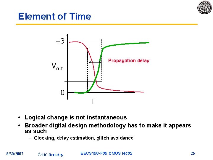
Element of Time +3 Propagation delay Vout 0 T • Logical change is not instantaneous • Broader digital design methodology has to make it appears as such – Clocking, delay estimation, glitch avoidance 8/30/2007 © UC Berkeley EECS 150 -F 05 CMOS lec 02 26

Announcements u. Reading assignment for this week. u. Katz and Boriello, Chap 1 u. K&B 2. 1 -2. 3, pp. 155 -172 u. Homework 1 is posted - due week from friday 8/30/2007 © UC Berkeley EECS 150 -F 05 CMOS lec 02 27

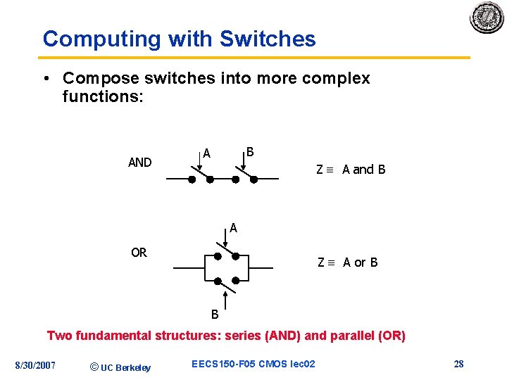
Computing with Switches • Compose switches into more complex functions: AND B A Z A and B A OR Z A or B B Two fundamental structures: series (AND) and parallel (OR) 8/30/2007 © UC Berkeley EECS 150 -F 05 CMOS lec 02 28

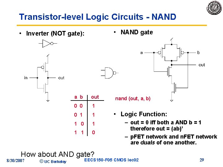
Transistor-level Logic Circuits - NAND • NAND gate • Inverter (NOT gate): a b out 0 0 1 1 1 0 How about AND gate? 8/30/2007 © UC Berkeley nand (out, a, b) • Logic Function: – out = 0 iff both a AND b = 1 therefore out = (ab)’ – p. FET network and n. FET network are duals of one another. EECS 150 -F 05 CMOS lec 02 29

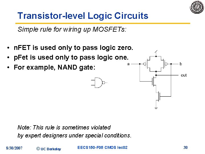
Transistor-level Logic Circuits Simple rule for wiring up MOSFETs: • n. FET is used only to pass logic zero. • p. Fet is used only to pass logic one. • For example, NAND gate: Note: This rule is sometimes violated by expert designers under special conditions. 8/30/2007 © UC Berkeley EECS 150 -F 05 CMOS lec 02 30

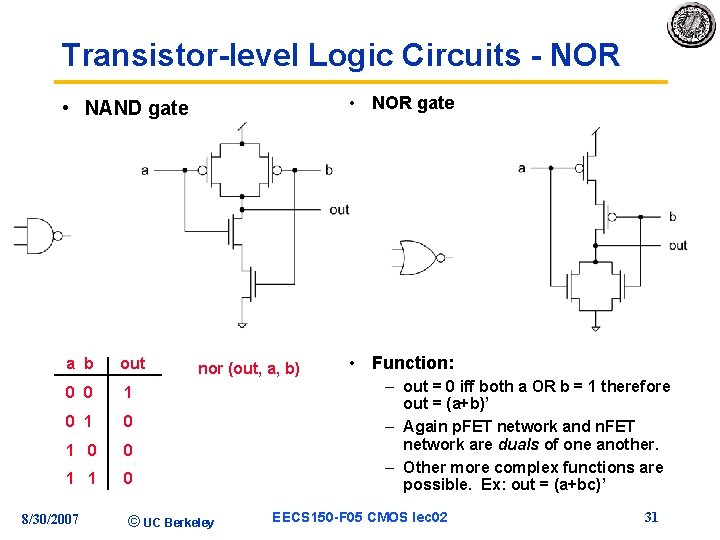
Transistor-level Logic Circuits - NOR • NOR gate • NAND gate a b out 0 0 1 0 1 0 0 1 1 0 8/30/2007 nor (out, a, b) © UC Berkeley • Function: – out = 0 iff both a OR b = 1 therefore out = (a+b)’ – Again p. FET network and n. FET network are duals of one another. – Other more complex functions are possible. Ex: out = (a+bc)’ EECS 150 -F 05 CMOS lec 02 31

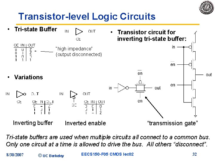
Transistor-level Logic Circuits • Tri-state Buffer • Transistor circuit for inverting tri-state buffer: “high impedance” (output disconnected) • Variations Inverting buffer Inverted enable “transmission gate” Tri-state buffers are used when multiple circuits all connect to a common bus. Only one circuit at a time is allowed to drive the bus. All others “disconnect”. 8/30/2007 © UC Berkeley EECS 150 -F 05 CMOS lec 02 32

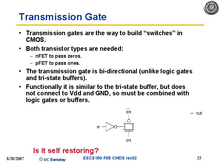
Transmission Gate • Transmission gates are the way to build “switches” in CMOS. • Both transistor types are needed: – n. FET to pass zeros. – p. FET to pass ones. • The transmission gate is bi-directional (unlike logic gates and tri-state buffers). • Functionally it is similar to the tri-state buffer, but does not connect to Vdd and GND, so must be combined with logic gates or buffers. Is it self restoring? 8/30/2007 © UC Berkeley EECS 150 -F 05 CMOS lec 02 33

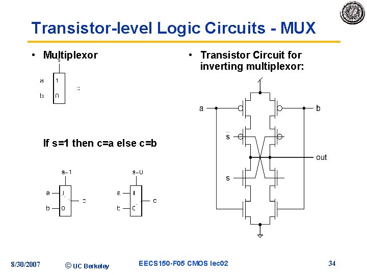
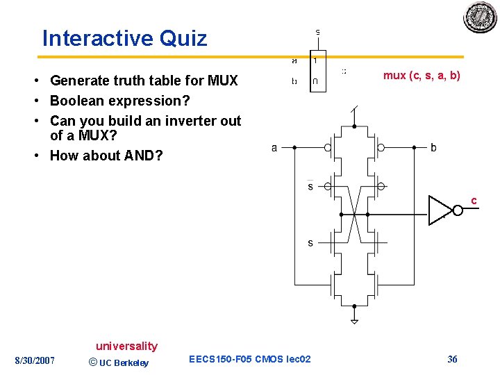
Transistor-level Logic Circuits - MUX • Multiplexor • Transistor Circuit for inverting multiplexor: If s=1 then c=a else c=b 8/30/2007 © UC Berkeley EECS 150 -F 05 CMOS lec 02 34

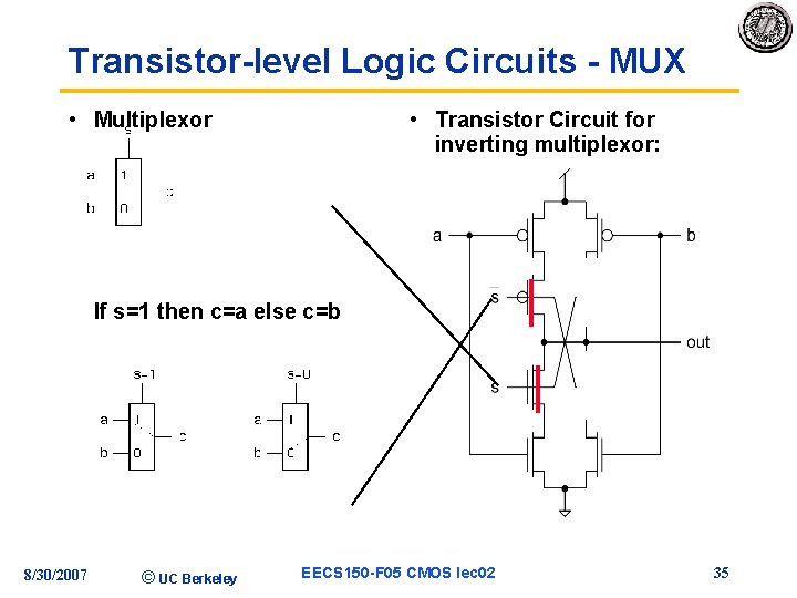
Transistor-level Logic Circuits - MUX • Multiplexor • Transistor Circuit for inverting multiplexor: If s=1 then c=a else c=b 8/30/2007 © UC Berkeley EECS 150 -F 05 CMOS lec 02 35

Interactive Quiz • Generate truth table for MUX • Boolean expression? • Can you build an inverter out of a MUX? • How about AND? mux (c, s, a, b) c 8/30/2007 universality © UC Berkeley EECS 150 -F 05 CMOS lec 02 36

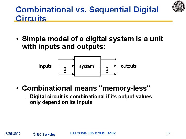
Combinational vs. Sequential Digital Circuits • Simple model of a digital system is a unit with inputs and outputs: inputs system outputs • Combinational means "memory-less" – Digital circuit is combinational if its output values only depend on its inputs 8/30/2007 © UC Berkeley EECS 150 -F 05 CMOS lec 02 37

Sequential logic • Sequential systems – Exhibit behaviors (output values) that depend on current as well as previous inputs • All real circuits are sequential – Outputs do not change instantaneously after an input change – Why not, and why is it then sequential? • Fundamental abstraction of digital design is to reason (mostly) about steady-state behaviors – Examine outputs only after sufficient time has elapsed for the system to make its required changes and settle down 8/30/2007 © UC Berkeley EECS 150 -F 05 CMOS lec 02 38

Synchronous sequential digital systems • Combinational circuit outputs depend only on current inputs – After sufficient time has elapsed • Sequential circuits have memory – Even after waiting for transient activity to finish • Steady-state abstraction: most designers use it when constructing sequential circuits: – Memory of system is its state – Changes in system state only allowed at specific times controlled by an external periodic signal (the clock) – Clock period is elapsed time between state changes sufficiently long so that system reaches steady-state before next state change at end of period 8/30/2007 © UC Berkeley EECS 150 -F 05 CMOS lec 02 39

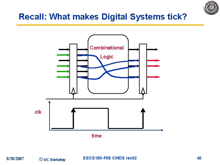
Recall: What makes Digital Systems tick? Combinational Logic clk time 8/30/2007 © UC Berkeley EECS 150 -F 05 CMOS lec 02 40

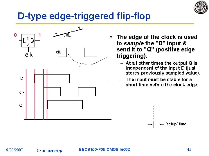
D-type edge-triggered flip-flop 0 1 0 1 0 • The edge of the clock is used to sample the "D" input & send it to "Q” (positive edge triggering). – At all other times the output Q is independent of the input D (just stores previously sampled value). – The input must be stable for a short time before the clock edge. 8/30/2007 © UC Berkeley EECS 150 -F 05 CMOS lec 02 41

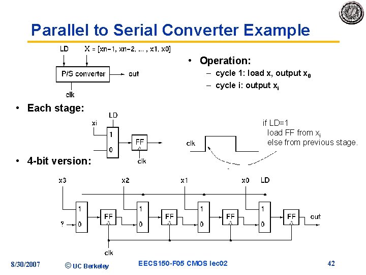
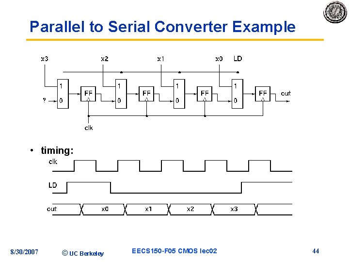
Parallel to Serial Converter Example • Operation: – cycle 1: load x, output x 0 – cycle i: output xi • Each stage: if LD=1 load FF from xi else from previous stage. • 4 -bit version: 8/30/2007 © UC Berkeley EECS 150 -F 05 CMOS lec 02 42

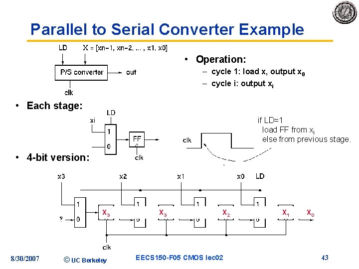
Parallel to Serial Converter Example • Operation: – cycle 1: load x, output x 0 – cycle i: output xi • Each stage: if LD=1 load FF from xi else from previous stage. • 4 -bit version: X 3 8/30/2007 © UC Berkeley XX 32 X X 21 EECS 150 -F 05 CMOS lec 02 X X 01 X 0 43

Parallel to Serial Converter Example • timing: 8/30/2007 © UC Berkeley EECS 150 -F 05 CMOS lec 02 44

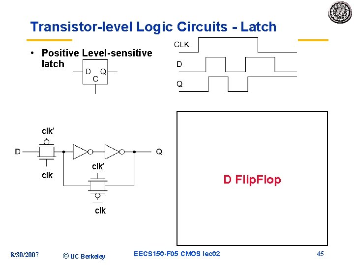
Transistor-level Logic Circuits - Latch • Positive Level-sensitive latch clk’ • Transistor Level clk • Positive Edge-triggered flip -flop built from two levelsensitive latches: clk’ D Flip. Flop clk 8/30/2007 © UC Berkeley EECS 150 -F 05 CMOS lec 02 45

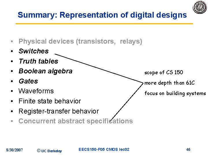
Summary: Representation of digital designs • • • Physical devices (transistors, relays) Switches Truth tables Boolean algebra Gates Waveforms Finite state behavior Register-transfer behavior Concurrent abstract specifications 8/30/2007 © UC Berkeley EECS 150 -F 05 CMOS lec 02 scope of CS 150 more depth than 61 C focus on building systems 46

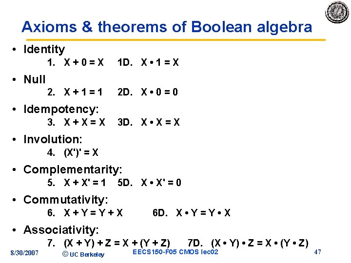
Axioms & theorems of Boolean algebra • Identity 1. X + 0 = X 1 D. X • 1 = X 2. X + 1 = 1 2 D. X • 0 = 0 • Null • Idempotency: 3. X + X = X 3 D. X • X = X • Involution: 4. (X')' = X • Complementarity: 5. X + X' = 1 5 D. X • X' = 0 • Commutativity: 6. X + Y = Y + X 6 D. X • Y = Y • X • Associativity: 7. (X + Y) + Z = X + (Y + Z) 8/30/2007 © UC Berkeley 7 D. (X • Y) • Z = X • (Y • Z) EECS 150 -F 05 CMOS lec 02 47

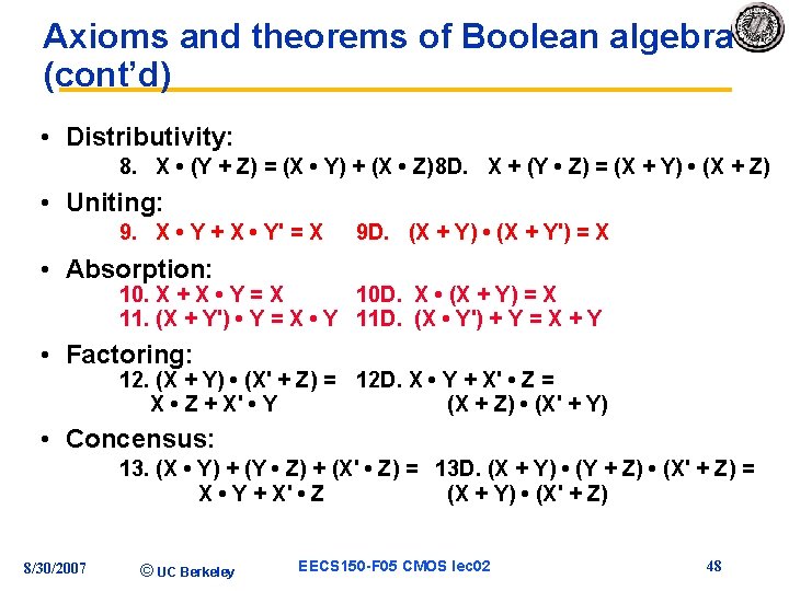
Axioms and theorems of Boolean algebra (cont’d) • Distributivity: 8. X • (Y + Z) = (X • Y) + (X • Z)8 D. X + (Y • Z) = (X + Y) • (X + Z) • Uniting: 9. X • Y + X • Y' = X 9 D. (X + Y) • (X + Y') = X • Absorption: 10. X + X • Y = X 10 D. X • (X + Y) = X 11. (X + Y') • Y = X • Y 11 D. (X • Y') + Y = X + Y • Factoring: 12. (X + Y) • (X' + Z) = 12 D. X • Y + X' • Z = X • Z + X' • Y (X + Z) • (X' + Y) • Concensus: 13. (X • Y) + (Y • Z) + (X' • Z) = 13 D. (X + Y) • (Y + Z) • (X' + Z) = X • Y + X' • Z (X + Y) • (X' + Z) 8/30/2007 © UC Berkeley EECS 150 -F 05 CMOS lec 02 48

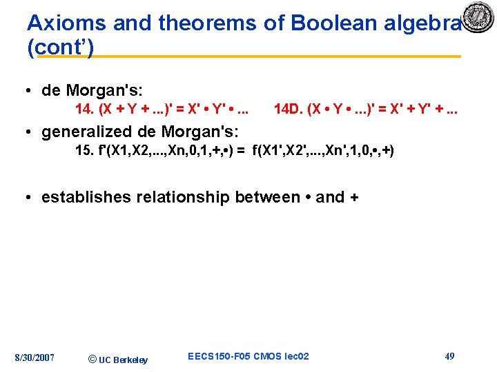
Axioms and theorems of Boolean algebra (cont’) • de Morgan's: 14. (X + Y +. . . )' = X' • Y' • . . . 14 D. (X • Y • . . . )' = X' + Y' +. . . • generalized de Morgan's: 15. f'(X 1, X 2, . . . , Xn, 0, 1, +, • ) = f(X 1', X 2', . . . , Xn', 1, 0, • , +) • establishes relationship between • and + 8/30/2007 © UC Berkeley EECS 150 -F 05 CMOS lec 02 49

Axioms & theorems of Bool. Alg. - Duality • Duality – Dual of a Boolean expression is derived by replacing • by +, + by • , 0 by 1, and 1 by 0, and leaving variables unchanged – Any theorem that can be proven is thus also proven for its dual! – Meta-theorem (a theorem about theorems) • duality: 16. X + Y +. . . X • Y • . . . • generalized duality: 17. f (X 1, X 2, . . . , Xn, 0, 1, +, • ) f(X 1, X 2, . . . , Xn, 1, 0, • , +) • Different than de. Morgan’s Law – this is a statement about theorems – this is not a way to manipulate (re-write) expressions 8/30/2007 © UC Berkeley EECS 150 -F 05 CMOS lec 02 50

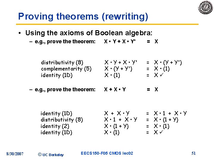
Proving theorems (rewriting) • Using the axioms of Boolean algebra: – e. g. , prove theorem: distributivity (8) complementarity (5) identity (1 D) – e. g. , prove theorem: identity (1 D) distributivity (8) identity (2) identity (1 D) 8/30/2007 © UC Berkeley X • Y + X • Y' = X X • Y + X • Y' X • (Y + Y') X • (1) = X • (Y + Y') = X • (1) = Xü X+X • Y = X X + X • Y X • 1 + X • Y X • (1 + Y) X • (1) = = EECS 150 -F 05 CMOS lec 02 X • 1 + X • Y X • (1 + Y) X • (1) Xü 51