
EEC 118 Lecture 7 Designing with Logical Effort
- Slides: 40
EEC 118 Lecture #7: Designing with Logical Effort Rajeevan Amirtharajah University of California, Davis Jeff Parkhurst Intel Corporation
Announcements • Lab 3 this week at lab section • HW 3 due this Friday at 4 PM in box, Kemper 2131 • Quizzes will be handed back in lab section Amirtharajah/Parkhurst, EEC 118 Spring 2011 2
Outline • Review: CMOS Combinational Gate Design • Finish Lecture 6 slides • Logical Effort • Combinational MOS Logic Circuits: Rabaey 6. 16. 2 (Kang & Leblebici, 7. 1 -7. 4) Amirtharajah/Parkhurst, EEC 118 Spring 2011 3
Acknowledgments • Slides due to David Money Harris from E 158: Introduction to CMOS VLSI Design at Harvey Mudd College Amirtharajah/Parkhurst, EEC 118 Spring 2011 4
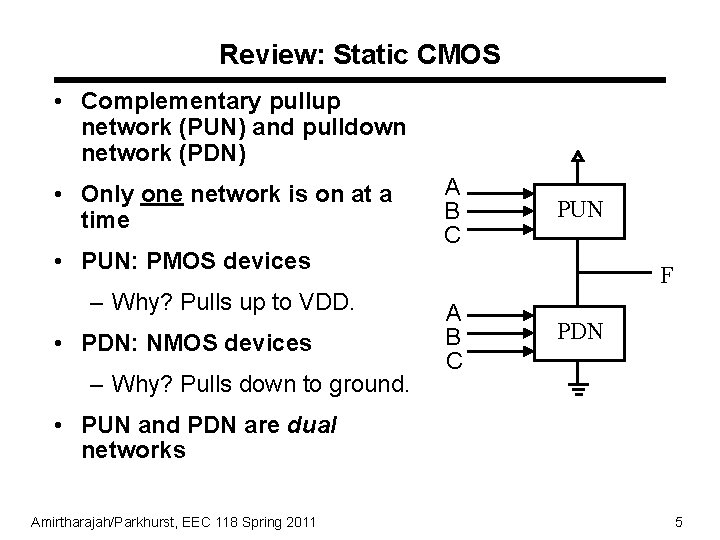
Review: Static CMOS • Complementary pullup network (PUN) and pulldown network (PDN) • Only one network is on at a time • PUN: PMOS devices – Why? Pulls up to VDD. • PDN: NMOS devices – Why? Pulls down to ground. A B C PUN F A B C PDN • PUN and PDN are dual networks Amirtharajah/Parkhurst, EEC 118 Spring 2011 5
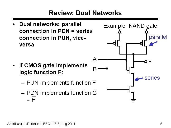
Review: Dual Networks • Dual networks: parallel connection in PDN = series connection in PUN, viceversa Example: NAND gate parallel A • If CMOS gate implements B logic function F: – PUN implements function F F series – PDN implements function G =F Amirtharajah/Parkhurst, EEC 118 Spring 2011 6
Lecture 6: Logical Effort Amirtharajah/Parkhurst, EEC 118 Spring 2011 7
Outline q q q Logical Effort Delay in a Logic Gate Multistage Logic Networks Choosing the Best Number of Stages Example Summary Amirtharajah/Parkhurst, EEC 118 Spring 2011 CMOS VLSI Design 4 th Ed. 8
Introduction q Chip designers face a bewildering array of choices – What is the best circuit topology for a function? – How many stages of logic give least delay? – How wide should the transistors be? q Logical effort is a method to make these decisions – Uses a simple model of delay – Allows back-of-the-envelope calculations – Helps make rapid comparisons between alternatives – Emphasizes remarkable symmetries Amirtharajah/Parkhurst, EEC 118 Spring 2011 CMOS VLSI Design 4 th Ed. 9
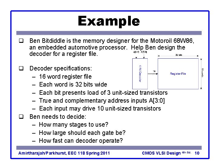
Example q Ben Bitdiddle is the memory designer for the Motoroil 68 W 86, an embedded automotive processor. Help Ben design the decoder for a register file. q Decoder specifications: – 16 word register file – Each word is 32 bits wide – Each bit presents load of 3 unit-sized transistors – True and complementary address inputs A[3: 0] – Each input may drive 10 unit-sized transistors q Ben needs to decide: – How many stages to use? – How large should each gate be? – How fast can decoder operate? Amirtharajah/Parkhurst, EEC 118 Spring 2011 CMOS VLSI Design 4 th Ed. 10
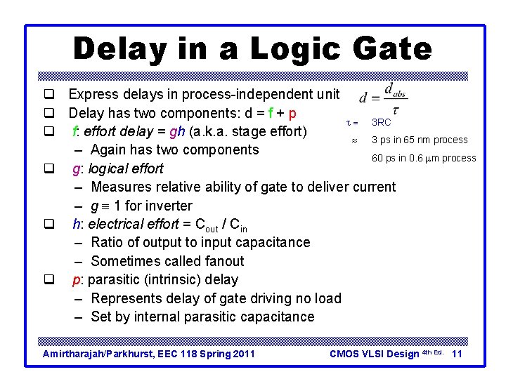
Delay in a Logic Gate q Express delays in process-independent unit q Delay has two components: d = f + p t = 3 RC q f: effort delay = gh (a. k. a. stage effort) 3 ps in 65 nm process – Again has two components 60 ps in 0. 6 mm process q g: logical effort – Measures relative ability of gate to deliver current – g 1 for inverter q h: electrical effort = Cout / Cin – Ratio of output to input capacitance – Sometimes called fanout q p: parasitic (intrinsic) delay – Represents delay of gate driving no load – Set by internal parasitic capacitance Amirtharajah/Parkhurst, EEC 118 Spring 2011 CMOS VLSI Design 4 th Ed. 11
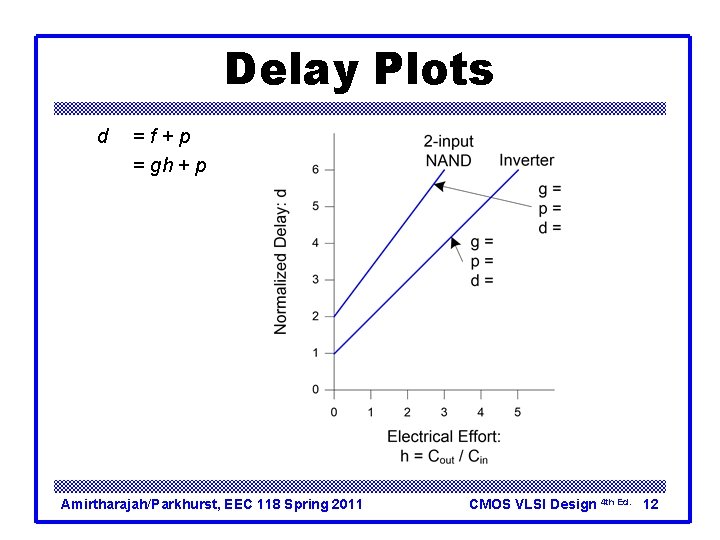
Delay Plots d =f+p = gh + p q What about NOR 2? Amirtharajah/Parkhurst, EEC 118 Spring 2011 CMOS VLSI Design 4 th Ed. 12
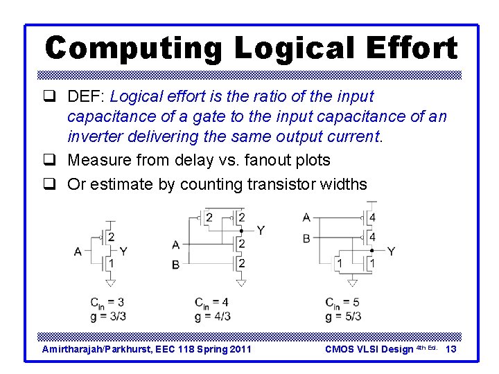
Computing Logical Effort q DEF: Logical effort is the ratio of the input capacitance of a gate to the input capacitance of an inverter delivering the same output current. q Measure from delay vs. fanout plots q Or estimate by counting transistor widths Amirtharajah/Parkhurst, EEC 118 Spring 2011 CMOS VLSI Design 4 th Ed. 13
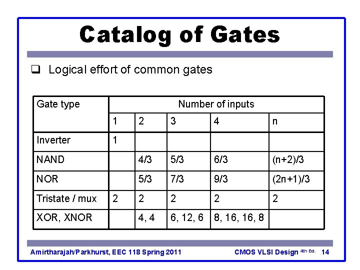
Catalog of Gates q Logical effort of common gates Gate type Number of inputs 1 2 3 4 n NAND 4/3 5/3 6/3 (n+2)/3 NOR 5/3 7/3 9/3 (2 n+1)/3 2 2 4, 4 6, 12, 6 8, 16, 8 Inverter Tristate / mux XOR, XNOR 1 2 Amirtharajah/Parkhurst, EEC 118 Spring 2011 CMOS VLSI Design 4 th Ed. 14
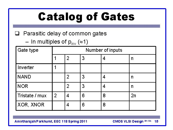
Catalog of Gates q Parasitic delay of common gates – In multiples of pinv ( 1) Gate type Number of inputs 1 2 3 4 n NAND 2 3 4 n NOR 2 3 4 n 4 6 8 2 n 4 6 8 Inverter Tristate / mux XOR, XNOR 1 2 Amirtharajah/Parkhurst, EEC 118 Spring 2011 CMOS VLSI Design 4 th Ed. 15
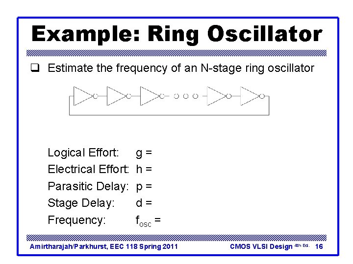
Example: Ring Oscillator q Estimate the frequency of an N-stage ring oscillator Logical Effort: Electrical Effort: Parasitic Delay: Stage Delay: Frequency: 31 stage ring oscillator in g=1 0. 6 mm process has h=1 frequency of ~ 200 MHz p=1 d=2 fosc = 1/(2*N*d) = 1/4 N Amirtharajah/Parkhurst, EEC 118 Spring 2011 CMOS VLSI Design 4 th Ed. 16
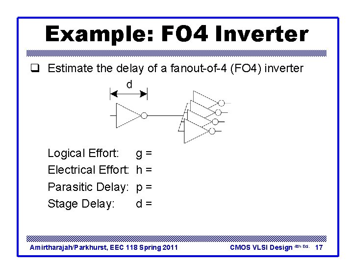
Example: FO 4 Inverter q Estimate the delay of a fanout-of-4 (FO 4) inverter Logical Effort: Electrical Effort: Parasitic Delay: Stage Delay: g=1 h=4 p=1 d=5 Amirtharajah/Parkhurst, EEC 118 Spring 2011 The FO 4 delay is about 300 ps in 0. 6 mm process 15 ps in a 65 nm process CMOS VLSI Design 4 th Ed. 17
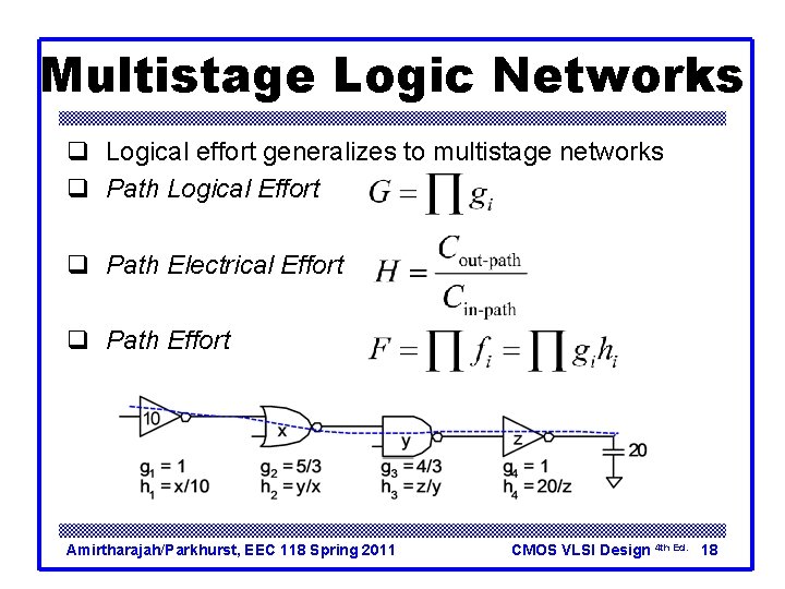
Multistage Logic Networks q Logical effort generalizes to multistage networks q Path Logical Effort q Path Electrical Effort q Path Effort Amirtharajah/Parkhurst, EEC 118 Spring 2011 CMOS VLSI Design 4 th Ed. 18
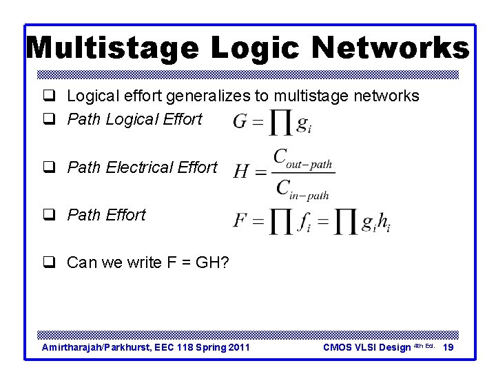
Multistage Logic Networks q Logical effort generalizes to multistage networks q Path Logical Effort q Path Electrical Effort q Path Effort q Can we write F = GH? Amirtharajah/Parkhurst, EEC 118 Spring 2011 CMOS VLSI Design 4 th Ed. 19
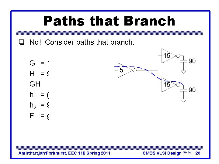
Paths that Branch q No! Consider paths that branch: G =1 H = 90 / 5 = 18 GH = 18 h 1 = (15 +15) / 5 = 6 h 2 = 90 / 15 = 6 F = g 1 g 2 h 1 h 2 = 36 = 2 GH Amirtharajah/Parkhurst, EEC 118 Spring 2011 CMOS VLSI Design 4 th Ed. 20
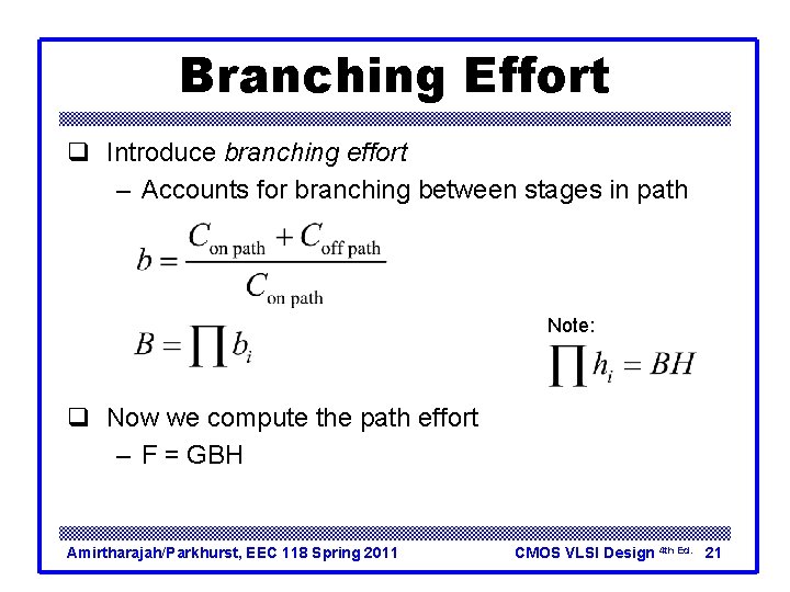
Branching Effort q Introduce branching effort – Accounts for branching between stages in path Note: q Now we compute the path effort – F = GBH Amirtharajah/Parkhurst, EEC 118 Spring 2011 CMOS VLSI Design 4 th Ed. 21
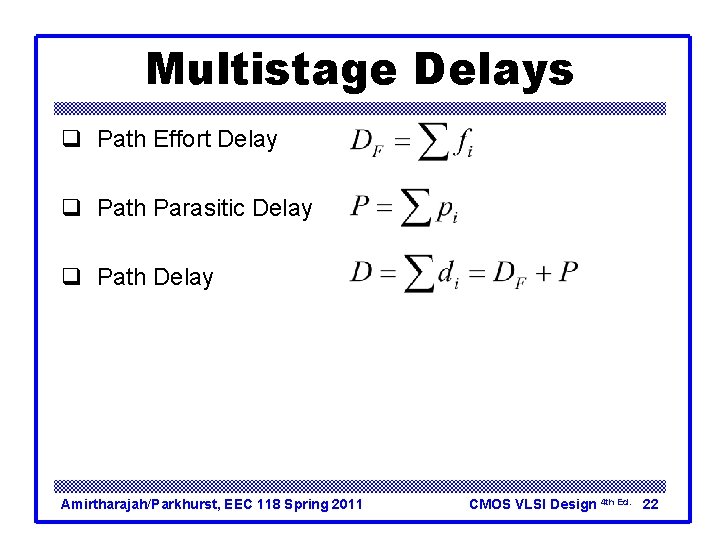
Multistage Delays q Path Effort Delay q Path Parasitic Delay q Path Delay Amirtharajah/Parkhurst, EEC 118 Spring 2011 CMOS VLSI Design 4 th Ed. 22
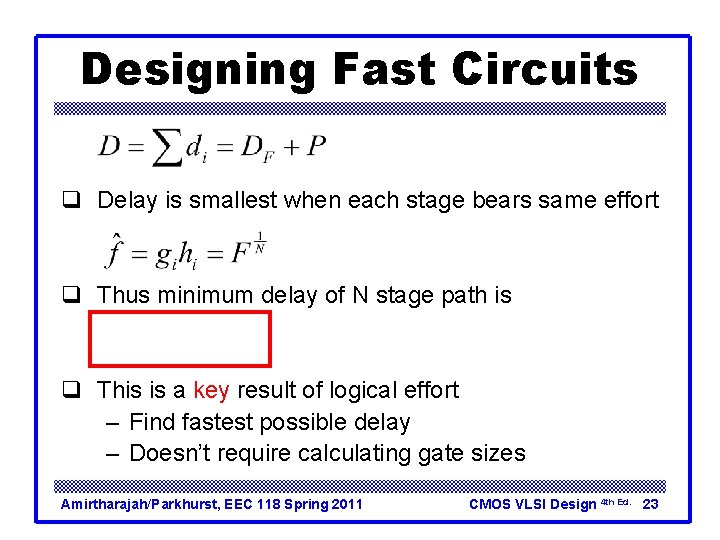
Designing Fast Circuits q Delay is smallest when each stage bears same effort q Thus minimum delay of N stage path is q This is a key result of logical effort – Find fastest possible delay – Doesn’t require calculating gate sizes Amirtharajah/Parkhurst, EEC 118 Spring 2011 CMOS VLSI Design 4 th Ed. 23
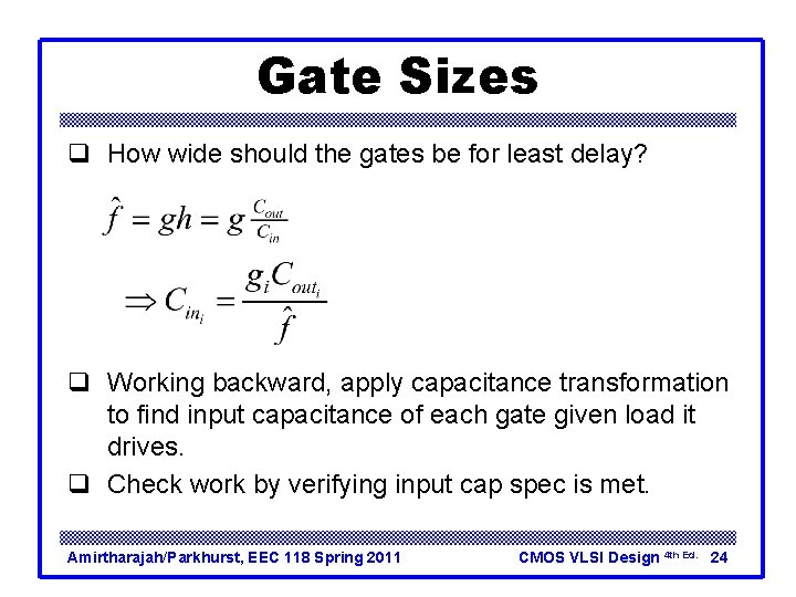
Gate Sizes q How wide should the gates be for least delay? q Working backward, apply capacitance transformation to find input capacitance of each gate given load it drives. q Check work by verifying input cap spec is met. Amirtharajah/Parkhurst, EEC 118 Spring 2011 CMOS VLSI Design 4 th Ed. 24
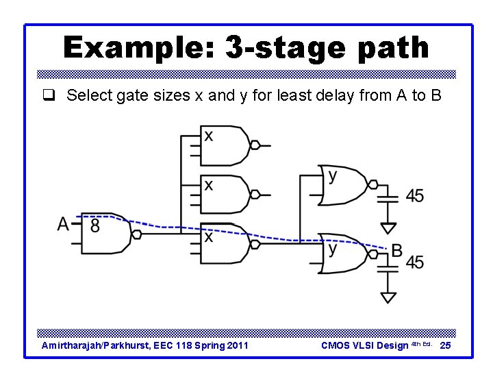
Example: 3 -stage path q Select gate sizes x and y for least delay from A to B Amirtharajah/Parkhurst, EEC 118 Spring 2011 CMOS VLSI Design 4 th Ed. 25
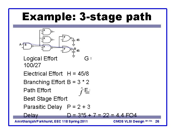
Example: 3 -stage path Logical Effort G = (4/3)*(5/3) = 100/27 Electrical Effort H = 45/8 Branching Effort B = 3 * 2 = 6 Path Effort F = GBH = 125 Best Stage Effort Parasitic Delay P = 2 + 3 + 2 = 7 Delay D = 3*5 + 7 = 22 = 4. 4 FO 4 Amirtharajah/Parkhurst, EEC 118 Spring 2011 CMOS VLSI Design 4 th Ed. 26
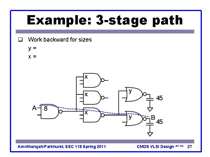
Example: 3 -stage path q Work backward for sizes y = 45 * (5/3) / 5 = 15 x = (15*2) * (5/3) / 5 = 10 Amirtharajah/Parkhurst, EEC 118 Spring 2011 CMOS VLSI Design 4 th Ed. 27
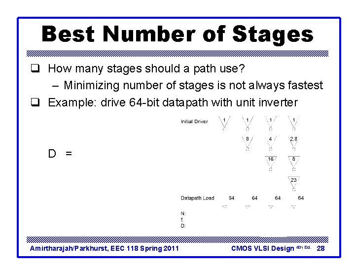
Best Number of Stages q How many stages should a path use? – Minimizing number of stages is not always fastest q Example: drive 64 -bit datapath with unit inverter D = NF 1/N + P = N(64)1/N + N Amirtharajah/Parkhurst, EEC 118 Spring 2011 CMOS VLSI Design 4 th Ed. 28
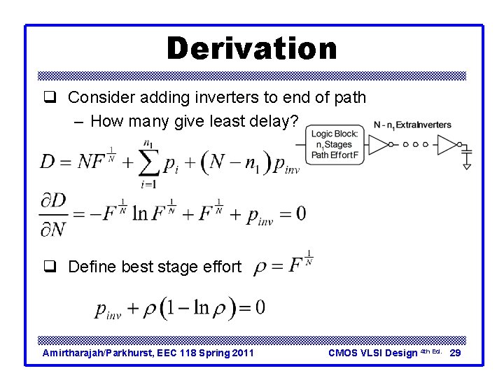
Derivation q Consider adding inverters to end of path – How many give least delay? q Define best stage effort Amirtharajah/Parkhurst, EEC 118 Spring 2011 CMOS VLSI Design 4 th Ed. 29
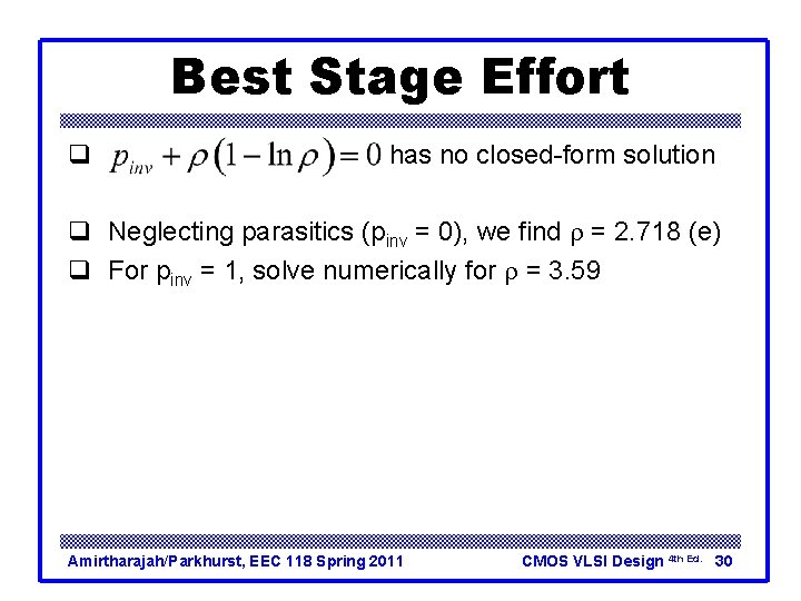
Best Stage Effort q has no closed-form solution q Neglecting parasitics (pinv = 0), we find r = 2. 718 (e) q For pinv = 1, solve numerically for r = 3. 59 Amirtharajah/Parkhurst, EEC 118 Spring 2011 CMOS VLSI Design 4 th Ed. 30
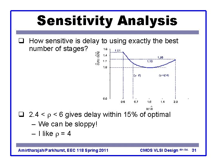
Sensitivity Analysis q How sensitive is delay to using exactly the best number of stages? q 2. 4 < r < 6 gives delay within 15% of optimal – We can be sloppy! – I like r = 4 Amirtharajah/Parkhurst, EEC 118 Spring 2011 CMOS VLSI Design 4 th Ed. 31
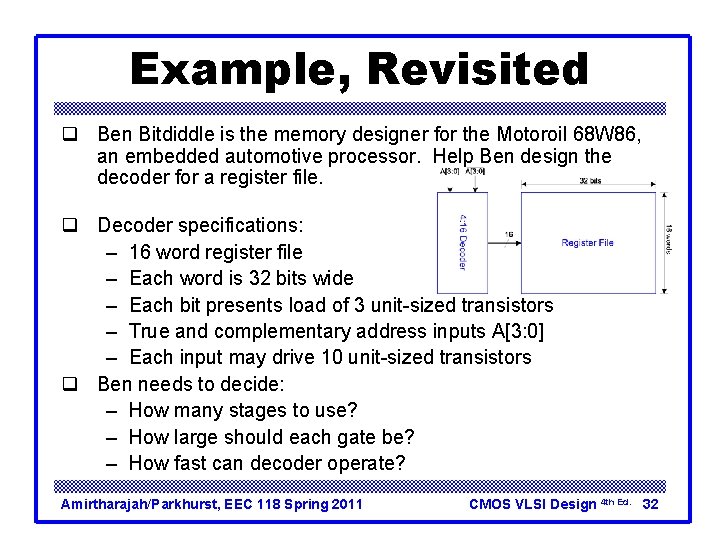
Example, Revisited q Ben Bitdiddle is the memory designer for the Motoroil 68 W 86, an embedded automotive processor. Help Ben design the decoder for a register file. q Decoder specifications: – 16 word register file – Each word is 32 bits wide – Each bit presents load of 3 unit-sized transistors – True and complementary address inputs A[3: 0] – Each input may drive 10 unit-sized transistors q Ben needs to decide: – How many stages to use? – How large should each gate be? – How fast can decoder operate? Amirtharajah/Parkhurst, EEC 118 Spring 2011 CMOS VLSI Design 4 th Ed. 32
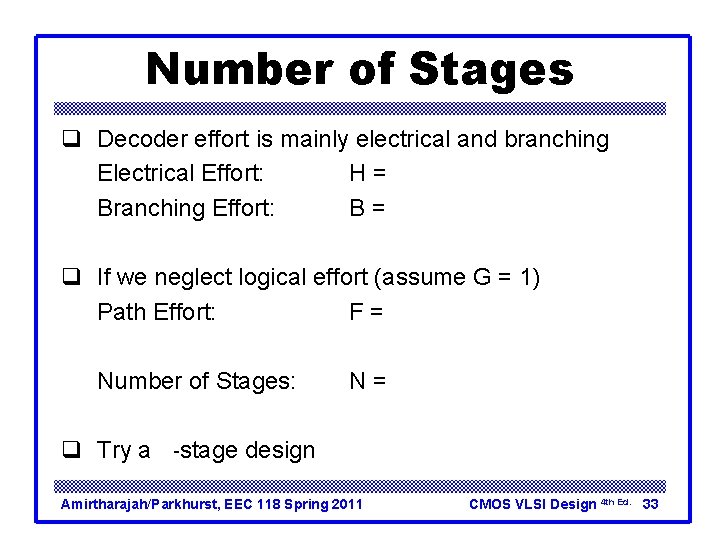
Number of Stages q Decoder effort is mainly electrical and branching Electrical Effort: H = (32*3) / 10 = 9. 6 Branching Effort: B=8 q If we neglect logical effort (assume G = 1) Path Effort: F = GBH = 76. 8 Number of Stages: N = log 4 F = 3. 1 q Try a 3 -stage design Amirtharajah/Parkhurst, EEC 118 Spring 2011 CMOS VLSI Design 4 th Ed. 33
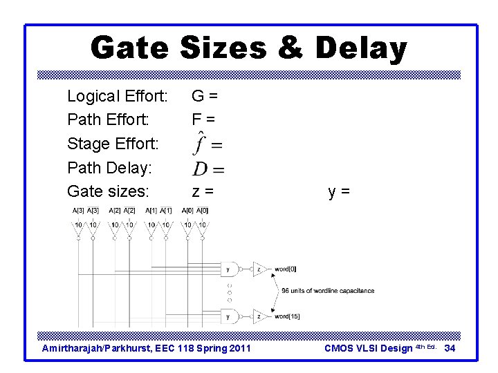
Gate Sizes & Delay Logical Effort: Path Effort: Stage Effort: Path Delay: Gate sizes: G = 1 * 6/3 * 1 = 2 F = GBH = 154 z = 96*1/5. 36 = 18 Amirtharajah/Parkhurst, EEC 118 Spring 2011 y = 18*2/5. 36 = 6. 7 CMOS VLSI Design 4 th Ed. 34
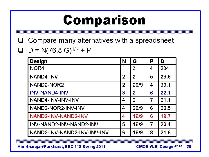
Comparison q Compare many alternatives with a spreadsheet q D = N(76. 8 G)1/N + P Design NOR 4 N 1 G 3 P 4 D 234 NAND 4 -INV 2 2 5 29. 8 NAND 2 -NOR 2 2 20/9 4 30. 1 INV-NAND 4 -INV-INV 3 4 2 2 6 7 22. 1 21. 1 NAND 2 -NOR 2 -INV 4 20/9 6 20. 5 NAND 2 -INV-NAND 2 -INV 4 16/9 6 19. 7 INV-NAND 2 -INV 5 16/9 7 20. 4 NAND 2 -INV-INV-INV 6 16/9 8 21. 6 Amirtharajah/Parkhurst, EEC 118 Spring 2011 CMOS VLSI Design 4 th Ed. 35
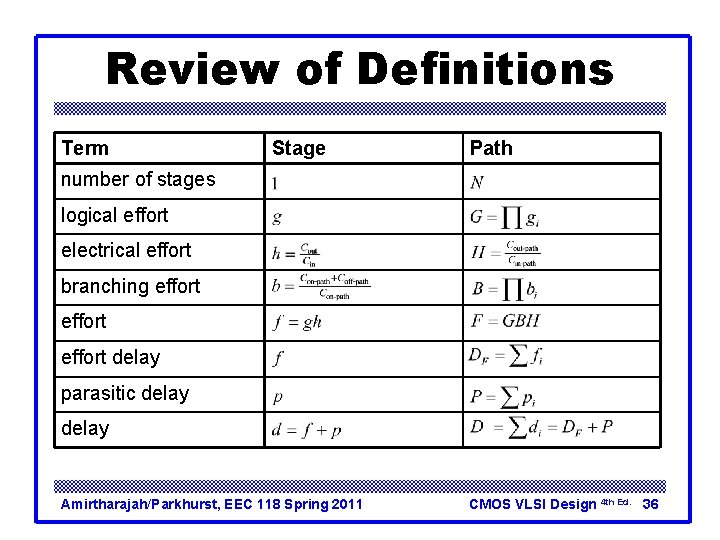
Review of Definitions Term Stage Path number of stages logical effort electrical effort branching effort delay parasitic delay Amirtharajah/Parkhurst, EEC 118 Spring 2011 CMOS VLSI Design 4 th Ed. 36
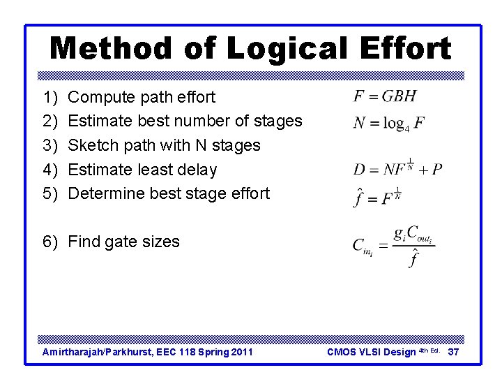
Method of Logical Effort 1) 2) 3) 4) 5) Compute path effort Estimate best number of stages Sketch path with N stages Estimate least delay Determine best stage effort 6) Find gate sizes Amirtharajah/Parkhurst, EEC 118 Spring 2011 CMOS VLSI Design 4 th Ed. 37
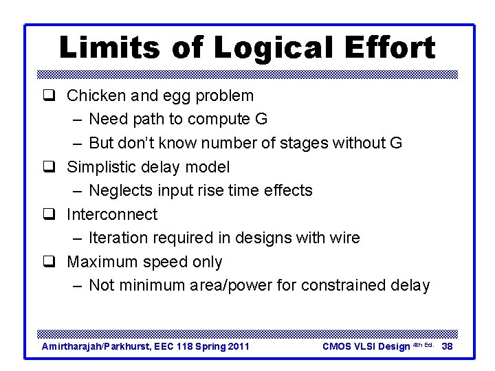
Limits of Logical Effort q Chicken and egg problem – Need path to compute G – But don’t know number of stages without G q Simplistic delay model – Neglects input rise time effects q Interconnect – Iteration required in designs with wire q Maximum speed only – Not minimum area/power for constrained delay Amirtharajah/Parkhurst, EEC 118 Spring 2011 CMOS VLSI Design 4 th Ed. 38
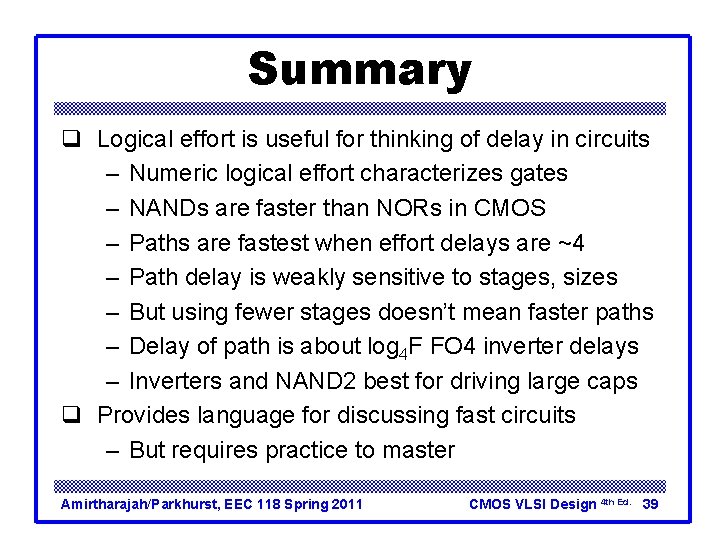
Summary q Logical effort is useful for thinking of delay in circuits – Numeric logical effort characterizes gates – NANDs are faster than NORs in CMOS – Paths are fastest when effort delays are ~4 – Path delay is weakly sensitive to stages, sizes – But using fewer stages doesn’t mean faster paths – Delay of path is about log 4 F FO 4 inverter delays – Inverters and NAND 2 best for driving large caps q Provides language for discussing fast circuits – But requires practice to master Amirtharajah/Parkhurst, EEC 118 Spring 2011 CMOS VLSI Design 4 th Ed. 39
Next Topic: Sequential Logic • Basic sequential circuits in CMOS – RS latches, transparent latches, flip-flops – Alternative sequential element topologies – Pipelining Amirtharajah/Parkhurst, EEC 118 Spring 2011 40