EE382 M VLSIII Circuits Design for Low Power


- Slides: 53

EE-382 M VLSI–II Circuits Design for Low Power Kevin Nowka, IBM Austin Research Laboratory EE 382 M VLSI-II Class Notes Foil # 1 The University of Texas at Austin

Agenda Overview of VLSI power Technology, Scaling, and Power Review of scaling A look at the real trends and projections for the future Active power – components, trends, managing, estimating Static power – components, trends, managing, estimating Summary EE 382 M VLSI-II Class Notes Foil # 2 The University of Texas at Austin

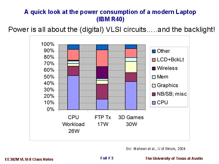
A quick look at the power consumption of a modern Laptop (IBM R 40) Power is all about the (digital) VLSI circuits…. . and the backlight! Src: Mahesri et al. , U of Illinois, 2004 EE 382 M VLSI-II Class Notes Foil # 3 The University of Texas at Austin

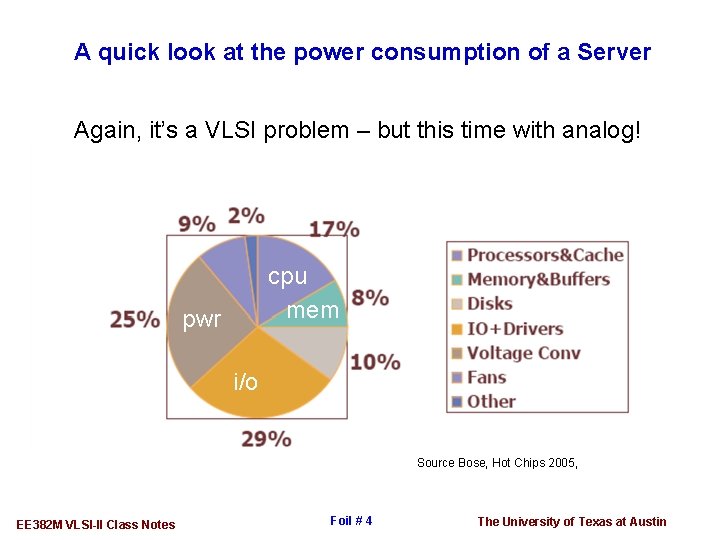
A quick look at the power consumption of a Server Again, it’s a VLSI problem – but this time with analog! cpu mem pwr i/o Source Bose, Hot Chips 2005, EE 382 M VLSI-II Class Notes Foil # 4 The University of Texas at Austin

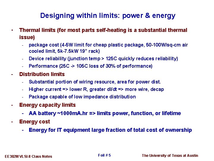
Designing within limits: power & energy • - - Thermal limits (for most parts self-heating is a substantial thermal issue) - package cost (4 -5 W limit for cheap plastic package, 50 -100 W/sq-cm air cooled limit, 5 k-7. 5 k. W 19” rack) - Device reliability (junction temp > 125 C quickly reduces reliability) - Performance (25 C -> 105 C loss of 30% of performance) Distribution limits - Substantial portion of wiring resource, area for power dist. - Higher current => lower R, greater d. I/dt => more wire, decap - Package capable of low impedance distribution Energy capacity limits - AA battery ~1000 m. A. hr => limits power, function, or lifetime - Energy cost - Energy for IT equipment large fraction of total cost of ownership EE 382 M VLSI-II Class Notes Foil # 5 The University of Texas at Austin

Agenda Overview of VLSI power Technology, Scaling, and Power Review of scaling A look at the real trends and projections for the future Active power – components, trends, managing, estimating Static power – components, trends, managing, estimating Summary EE 382 M VLSI-II Class Notes Foil # 6 The University of Texas at Austin

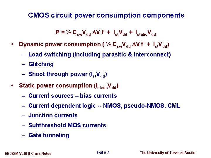
CMOS circuit power consumption components P = ½ Csw. Vdd DV f + Ist. Vdd + Istatic. Vdd • Dynamic power consumption ( ½ Csw. Vdd DV f + Ist. Vdd) – Load switching (including parasitic & interconnect) – Glitching – Shoot through power (Ist. Vdd) • Static power consumption (Istatic. Vdd) – Current sources – bias currents – Current dependent logic -- NMOS, pseudo-NMOS, CML – Junction currents – Subthreshold MOS currents – Gate tunneling EE 382 M VLSI-II Class Notes Foil # 7 The University of Texas at Austin

Review of Constant Field Scaling Scale factor a<1 EE 382 M VLSI-II Class Notes Parameter Value Scaled Value Dimensions L, W, Tox a. L, a. W, a. Tox Dopant concentrations Na, Nd Na/a, Nd/a Voltage V a. V Field E E Capacitance C a. C Current I a. I Propagation time (~CV/I) t at Power (VI) P a 2 P Density d d/a 2 Power density P/A Foil # 8 These are distributions… how do the s s scale? The University of Texas at Austin

Agenda Overview of VLSI power Technology, Scaling, and Power Review of scaling A look at the real trends and projections for the future Active power – components, trends, managing, estimating Static power – components, trends, managing, estimating Summary EE 382 M VLSI-II Class Notes Foil # 9 The University of Texas at Austin

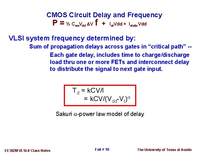
CMOS Circuit Delay and Frequency P = ½ Csw. Vdd DV f + Ist. Vdd + Istatic. Vdd VLSI system frequency determined by: Sum of propagation delays across gates in “critical path” -Each gate delay, includes time to charge/discharge load thru one or more FETs and interconnect delay to distribute the signal to next gate input. Td = k. CV/I = k. CV/(Vdd-Vt)a Sakuri a-power law model of delay EE 382 M VLSI-II Class Notes Foil # 10 The University of Texas at Austin

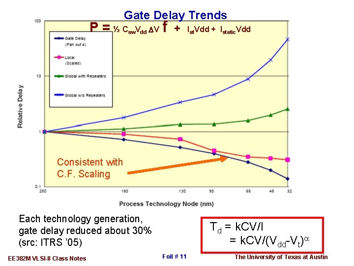
Gate Delay Trends P = ½ Csw. Vdd DV f + Ist. Vdd + Istatic. Vdd Consistent with C. F. Scaling Each technology generation, gate delay reduced about 30% (src: ITRS ’ 05) EE 382 M VLSI-II Class Notes Td = k. CV/I = k. CV/(Vdd-Vt)a Foil # 11 The University of Texas at Austin

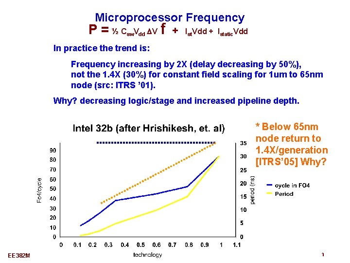
Microprocessor Frequency P = ½ Csw. Vdd DV f + Ist. Vdd + Istatic. Vdd In practice the trend is: Frequency increasing by 2 X (delay decreasing by 50%), not the 1. 4 X (30%) for constant field scaling for 1 um to 65 nm node (src: ITRS ’ 01). Why? decreasing logic/stage and increased pipeline depth. * Below 65 nm node return to 1. 4 X/generation [ITRS’ 05] Why? EE 382 M VLSI-II Class Notes Foil # 12 The University of Texas at Austin

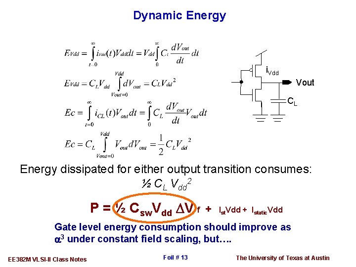
Dynamic Energy i. Vdd Vout CL Energy dissipated for either output transition consumes: ½ CL Vdd 2 P = ½ Csw. Vdd DV f + Ist. Vdd + Istatic. Vdd Gate level energy consumption should improve as a 3 under constant field scaling, but…. EE 382 M VLSI-II Class Notes Foil # 13 The University of Texas at Austin

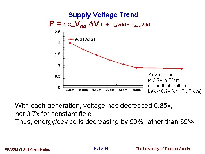
Supply Voltage Trend P = ½ Csw. Vdd DV f + Ist. Vdd + Istatic. Vdd Slow decline to 0. 7 V in 22 nm (some think nothing below 0. 9 V for HP u. Procs) With each generation, voltage has decreased 0. 85 x, not 0. 7 x for constant field. Thus, energy/device is decreasing by 50% rather than 65% EE 382 M VLSI-II Class Notes Foil # 14 The University of Texas at Austin

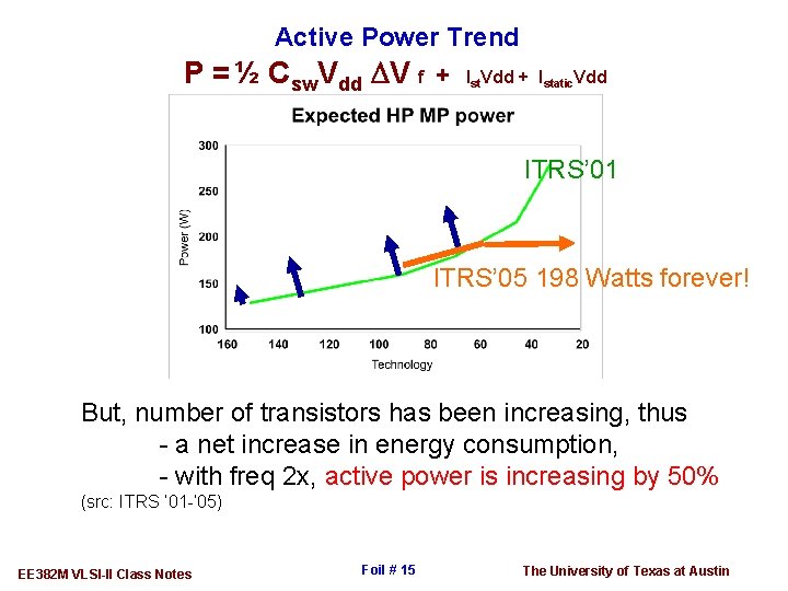
Active Power Trend P = ½ Csw. Vdd DV f + Ist. Vdd + Istatic. Vdd ITRS’ 01 ITRS’ 05 198 Watts forever! But, number of transistors has been increasing, thus - a net increase in energy consumption, - with freq 2 x, active power is increasing by 50% (src: ITRS ’ 01 -’ 05) EE 382 M VLSI-II Class Notes Foil # 15 The University of Texas at Austin

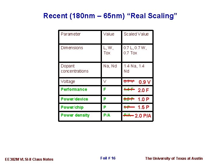
Recent (180 nm – 65 nm) “Real Scaling” EE 382 M VLSI-II Class Notes Parameter Value Scaled Value Dimensions L, W, Tox 0. 7 L, 0. 7 W, 0. 7 Tox Dopant concentrations Na, Nd 1. 4 Na, 1. 4 Nd Voltage V 0. 7 V 0. 9 V Performance F 1. 4 F 2. 0 F Power/device P 0. 5 P 1. 0 P Power/chip P 1 P 1. 5 P Power density P/A 2. 0 P/A Foil # 16 The University of Texas at Austin

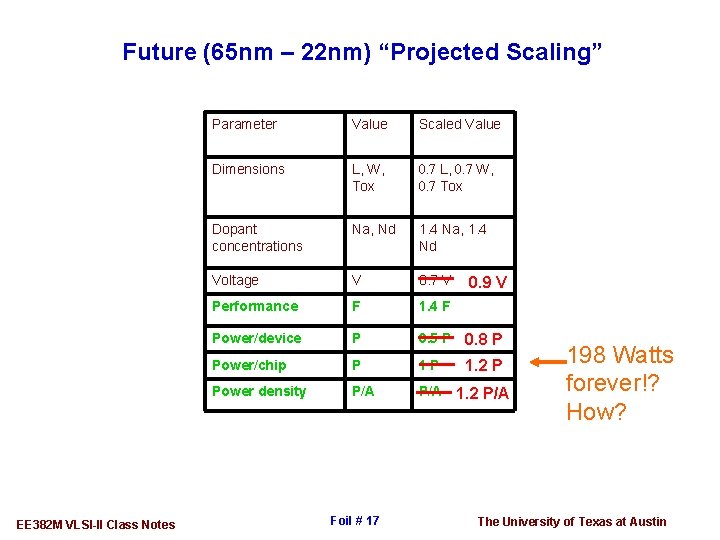
Future (65 nm – 22 nm) “Projected Scaling” EE 382 M VLSI-II Class Notes Parameter Value Scaled Value Dimensions L, W, Tox 0. 7 L, 0. 7 W, 0. 7 Tox Dopant concentrations Na, Nd 1. 4 Na, 1. 4 Nd Voltage V 0. 7 V Performance F 1. 4 F Power/device P 0. 5 P 0. 8 P Power/chip P 1 P 1. 2 P Power density P/A 1. 2 P/A Foil # 17 0. 9 V 198 Watts forever!? How? The University of Texas at Austin

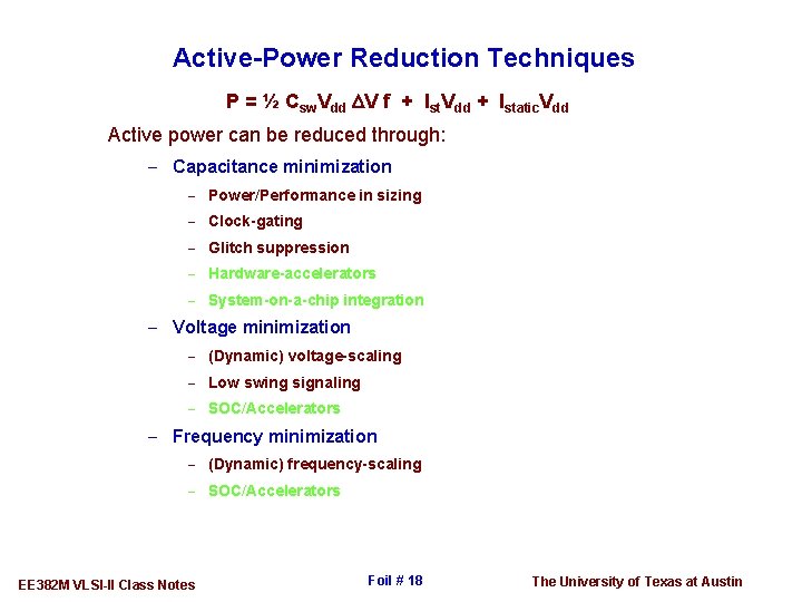
Active-Power Reduction Techniques P = ½ Csw. Vdd DV f + Ist. Vdd + Istatic. Vdd Active power can be reduced through: - Capacitance minimization - Power/Performance in sizing - Clock-gating - Glitch suppression - Hardware-accelerators - System-on-a-chip integration - Voltage minimization - (Dynamic) voltage-scaling - Low swing signaling - SOC/Accelerators - Frequency minimization - (Dynamic) frequency-scaling - SOC/Accelerators EE 382 M VLSI-II Class Notes Foil # 18 The University of Texas at Austin

Capacitance minimization P = ½ Csw. Vdd DV f + Ist. Vdd + Istatic. Vdd Only the devices (device width) used in the design consume active power! - Runs counter to the complexity-for-IPC trend - Runs counter to the SOC trend EE 382 M VLSI-II Class Notes Foil # 19 The University of Texas at Austin

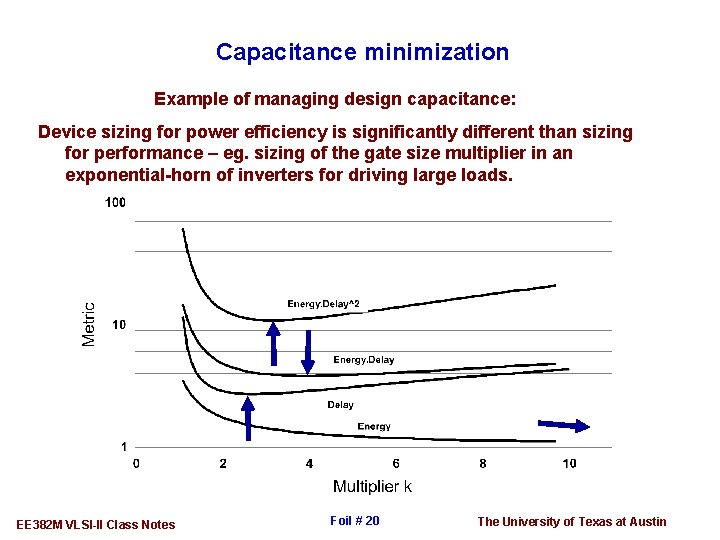
Capacitance minimization Example of managing design capacitance: Device sizing for power efficiency is significantly different than sizing for performance – eg. sizing of the gate size multiplier in an exponential-horn of inverters for driving large loads. EE 382 M VLSI-II Class Notes Foil # 20 The University of Texas at Austin

Functional Clock Gating P = ½ Csw. Vdd DV f + Ist. Vdd + Istatic. Vdd • 25 -50% of power consumption due to driving latches (Bose, Martinozi, Brooks 2001 50%) • Utilization of most latches is low (~10 -35%) • Gate off unused latches and associated logic: – Unit level clock gating – turn off clocks to FPU, MMX, Shifter, L/S unit, … at clk buffer or splitter – Functional clock gating – turn off clocks to individual latch banks – forwarding latch, shift-amount register, overflow logic & latches, …qualify (AND) clock to latch • Asynch is the most aggressive gating – but is it efficient? EE 382 M VLSI-II Class Notes Foil # 21 The University of Texas at Austin

Glitch suppression P = ½ Csw. Vdd DV f + Ist. Vdd + Istatic. Vdd • Glitches can represent a sizeable portion of active power, (up to 30% for some circuits in some studies) • Three basic mechanisms for avoidance: – Use non-glitching logic, e. g. domino – Add redundant logic to avoid glitching hazards • Increases cap, testability problems – Adjust delays in the design to avoid • Shouldn’t timing tools do this already if it is possible? EE 382 M VLSI-II Class Notes Foil # 22 The University of Texas at Austin

Voltage minimization P = ½ Csw. Vdd DV f + Ist. Vdd + Istatic. Vdd • Lowering voltage swing, DV, lowers power – Low swing logic efforts have not been very successful (unless you consider array voltage sensing) – Low swing busses have been quite successful • Lowering supply, Vdd and DV, (voltage scaling) is most promising: – Frequency ~V, Power ~V 3 EE 382 M VLSI-II Class Notes Foil # 23 The University of Texas at Austin

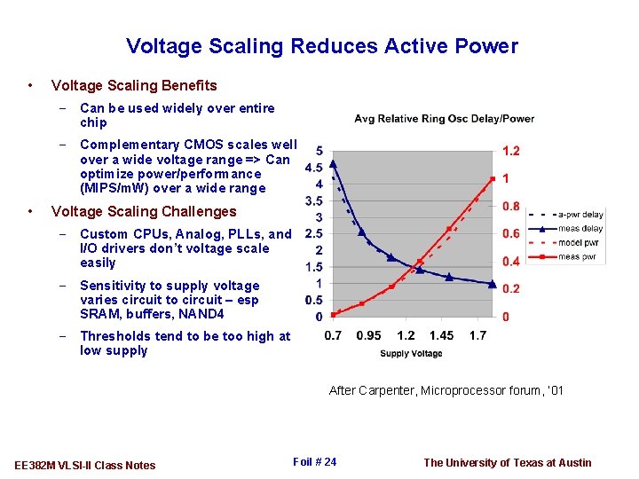
Voltage Scaling Reduces Active Power • Voltage Scaling Benefits - Can be used widely over entire chip - Complementary CMOS scales well over a wide voltage range => Can optimize power/performance (MIPS/m. W) over a wide range • Voltage Scaling Challenges - Custom CPUs, Analog, PLLs, and I/O drivers don’t voltage scale easily - Sensitivity to supply voltage varies circuit to circuit – esp SRAM, buffers, NAND 4 - Thresholds tend to be too high at low supply After Carpenter, Microprocessor forum, ‘ 01 EE 382 M VLSI-II Class Notes Foil # 24 The University of Texas at Austin

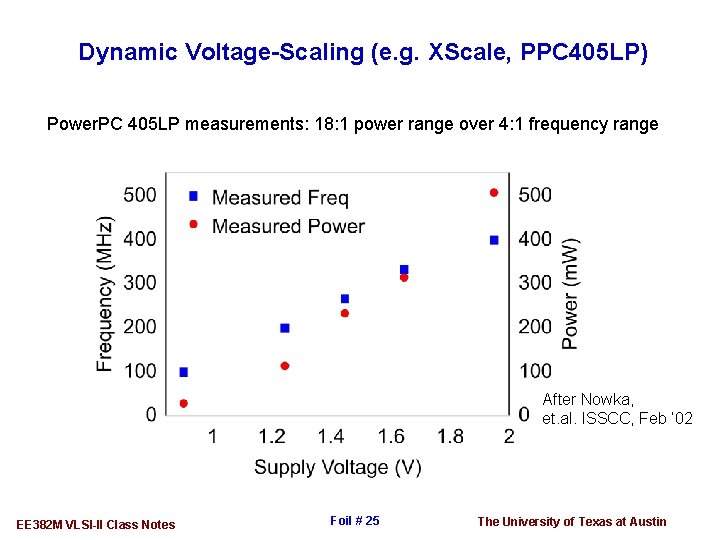
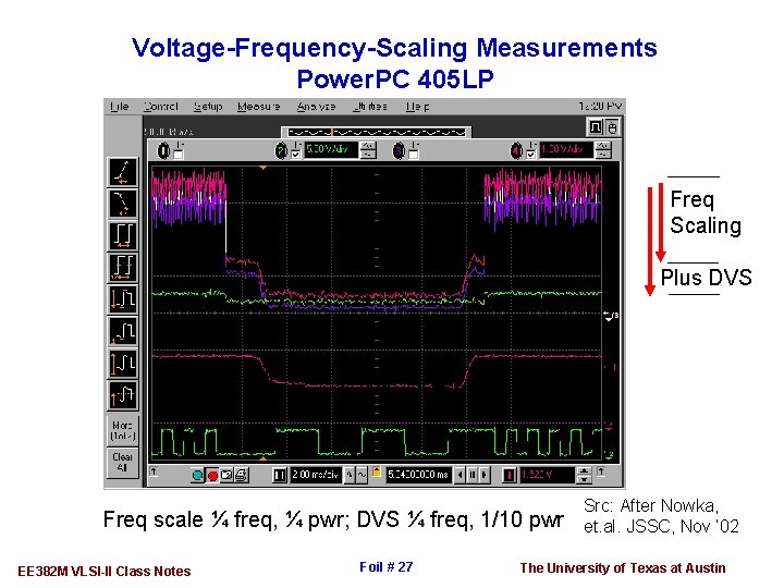
Dynamic Voltage-Scaling (e. g. XScale, PPC 405 LP) Power. PC 405 LP measurements: 18: 1 power range over 4: 1 frequency range After Nowka, et. al. ISSCC, Feb ‘ 02 EE 382 M VLSI-II Class Notes Foil # 25 The University of Texas at Austin

Frequency minimization P = ½ Csw. Vdd DV f + Ist. Vdd + Istatic. Vdd • Lowering frequency lowers power linearly – DOES NOT improve energy efficiency, just slows down energy consumption – Important for avoiding thermal problems EE 382 M VLSI-II Class Notes Foil # 26 The University of Texas at Austin

Voltage-Frequency-Scaling Measurements Power. PC 405 LP Freq Scaling Plus DVS Freq scale ¼ freq, ¼ pwr; DVS ¼ freq, 1/10 pwr EE 382 M VLSI-II Class Notes Foil # 27 Src: After Nowka, et. al. JSSC, Nov ‘ 02 The University of Texas at Austin

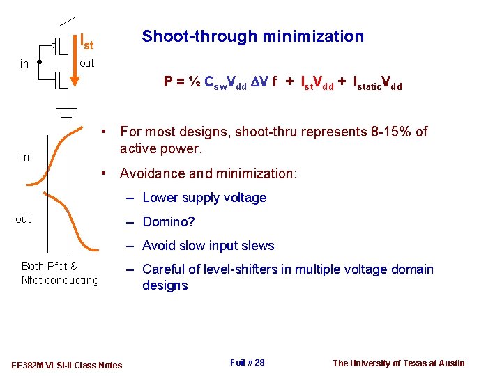
Shoot-through minimization Ist in out P = ½ Csw. Vdd DV f + Ist. Vdd + Istatic. Vdd in • For most designs, shoot-thru represents 8 -15% of active power. • Avoidance and minimization: – Lower supply voltage out – Domino? – Avoid slow input slews Both Pfet & Nfet conducting EE 382 M VLSI-II Class Notes – Careful of level-shifters in multiple voltage domain designs Foil # 28 The University of Texas at Austin

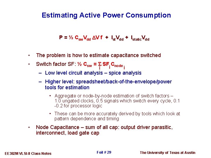
Estimating Active Power Consumption P = ½ Csw. Vdd DV f + Ist. Vdd + Istatic. Vdd • The problem is how to estimate capacitance switched • Switch factor SF: ½ Csw = S SF Cnode i i i – Low level circuit analysis – spice analysis – Higher level: spreadsheet/back-of-the-envelope/power tools for estimation • Aggregate or node-by-node estimation of switch factors – 1. 0 ungated clocks, 0. 5 signals which switch every cycle, 0. 1 -0. 2 for processor logic • These can be more accurately derived by tools which look at pattern dependence and timing • Node Capacitance – sum of all cap: output driver parasitic, interconnect, load gate cap EE 382 M VLSI-II Class Notes Foil # 29 The University of Texas at Austin

Agenda Overview of VLSI power Technology, Scaling, and Power Review of scaling A look at the real trends and projections for the future Active power – components, trends, managing, estimating Static power – components, trends, managing, estimating Summary EE 382 M VLSI-II Class Notes Foil # 30 The University of Texas at Austin

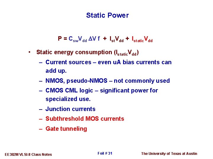
Static Power P = Csw. Vdd DV f + Ist. Vdd + Istatic. Vdd • Static energy consumption (Istatic. Vdd) – Current sources – even u. A bias currents can add up. – NMOS, pseudo-NMOS – not commonly used – CMOS CML logic – significant power for specialized use. – Junction currents – Subthreshold MOS currents – Gate tunneling EE 382 M VLSI-II Class Notes Foil # 31 The University of Texas at Austin

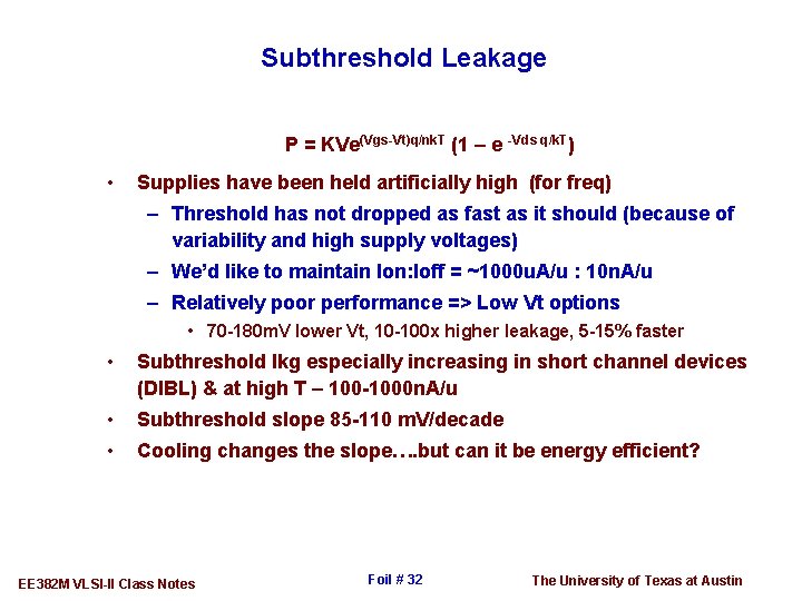
Subthreshold Leakage P = KVe(Vgs-Vt)q/nk. T (1 – e -Vds q/k. T) • Supplies have been held artificially high (for freq) – Threshold has not dropped as fast as it should (because of variability and high supply voltages) – We’d like to maintain Ion: Ioff = ~1000 u. A/u : 10 n. A/u – Relatively poor performance => Low Vt options • 70 -180 m. V lower Vt, 10 -100 x higher leakage, 5 -15% faster • Subthreshold lkg especially increasing in short channel devices (DIBL) & at high T – 100 -1000 n. A/u • Subthreshold slope 85 -110 m. V/decade • Cooling changes the slope…. but can it be energy efficient? EE 382 M VLSI-II Class Notes Foil # 32 The University of Texas at Austin

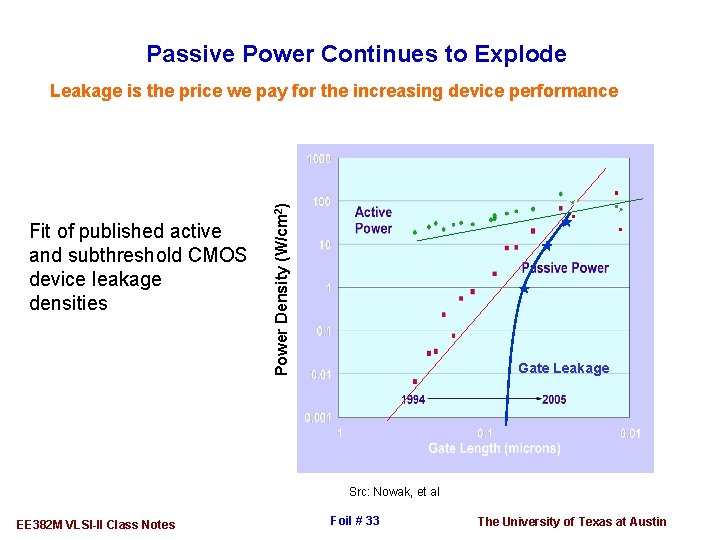
Passive Power Continues to Explode Fit of published active and subthreshold CMOS device leakage densities Power Density (W/cm 2) Leakage is the price we pay for the increasing device performance Gate Leakage Src: Nowak, et al EE 382 M VLSI-II Class Notes Foil # 33 The University of Texas at Austin

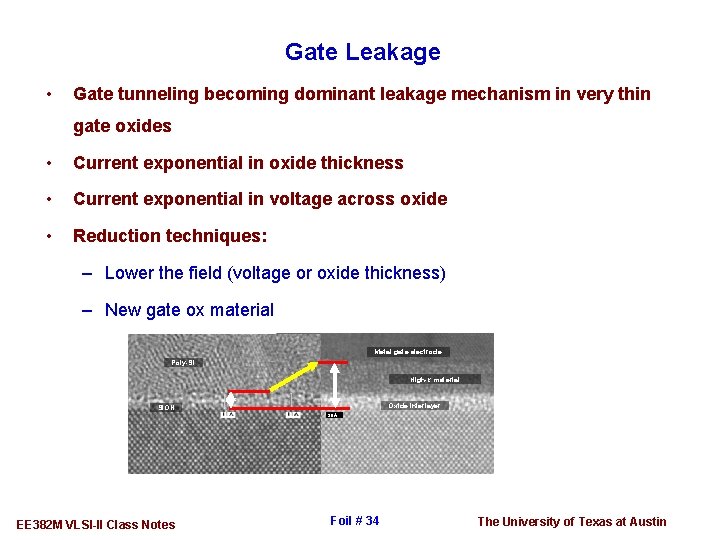
Gate Leakage • Gate tunneling becoming dominant leakage mechanism in very thin gate oxides • Current exponential in oxide thickness • Current exponential in voltage across oxide • Reduction techniques: – Lower the field (voltage or oxide thickness) – New gate ox material Metal gate electrode Poly-Si High-k material Oxide interlayer Si. ON 30 A EE 382 M VLSI-II Class Notes Foil # 34 The University of Texas at Austin

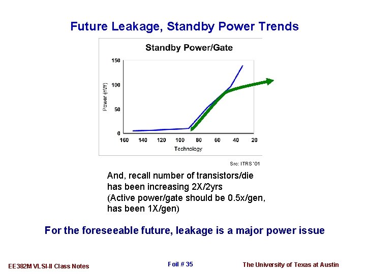
Future Leakage, Standby Power Trends Src: ITRS ‘ 01 And, recall number of transistors/die has been increasing 2 X/2 yrs (Active power/gate should be 0. 5 x/gen, has been 1 X/gen) For the foreseeable future, leakage is a major power issue EE 382 M VLSI-II Class Notes Foil # 35 The University of Texas at Austin

Standby-Power Reduction Techniques Standby power can be reduced through: - Capacitance minimization - Voltage-scaling - Power gating - Vdd/Vt selection EE 382 M VLSI-II Class Notes Foil # 36 The University of Texas at Austin

Capacitance minimization Only the devices (device width) used in the design leak! - Runs counter to the complexity-for-IPC trend - Runs counter to the SOC trend - Transistors are not free -- Even though they are not switched they still leak EE 382 M VLSI-II Class Notes Foil # 37 The University of Texas at Austin

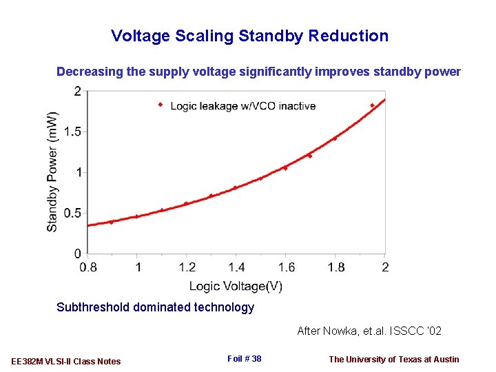
Voltage Scaling Standby Reduction Decreasing the supply voltage significantly improves standby power Subthreshold dominated technology After Nowka, et. al. ISSCC ‘ 02 EE 382 M VLSI-II Class Notes Foil # 38 The University of Texas at Austin

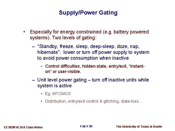
Supply/Power Gating • Especially for energy constrained (e. g. battery powered systems). Two levels of gating: – “Standby, freeze, sleep, deep-sleep, doze, nap, hibernate”: lower or turn off power supply to system to avoid power consumption when inactive • Control difficulties, hidden-state, entry/exit, “instanton” or user-visible. – Unit level power gating – turn off inactive units while system is active • Eg. MTCMOS • Distribution, entry/exit control & glitching, state-loss… EE 382 M VLSI-II Class Notes Foil # 39 The University of Texas at Austin

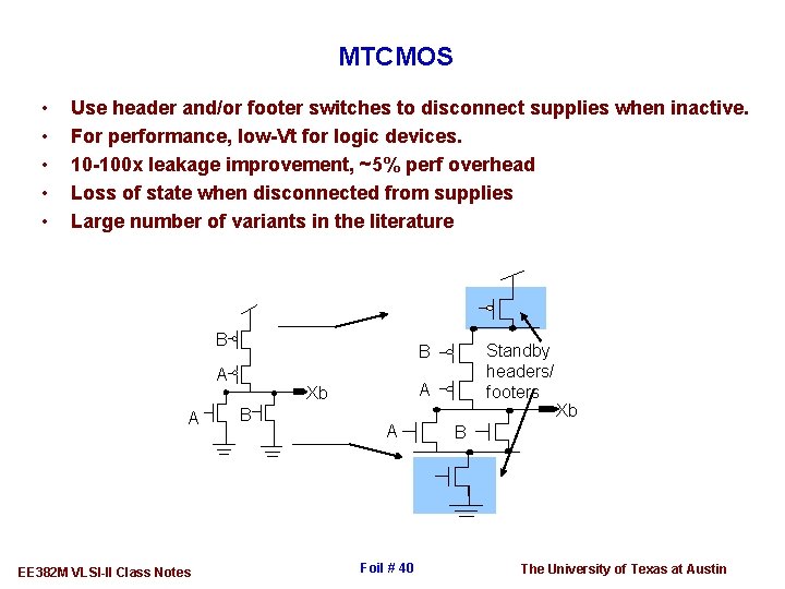
MTCMOS • • • Use header and/or footer switches to disconnect supplies when inactive. For performance, low-Vt for logic devices. 10 -100 x leakage improvement, ~5% perf overhead Loss of state when disconnected from supplies Large number of variants in the literature B A A EE 382 M VLSI-II Class Notes Standby headers/ footers B A Xb B A Foil # 40 Xb B The University of Texas at Austin

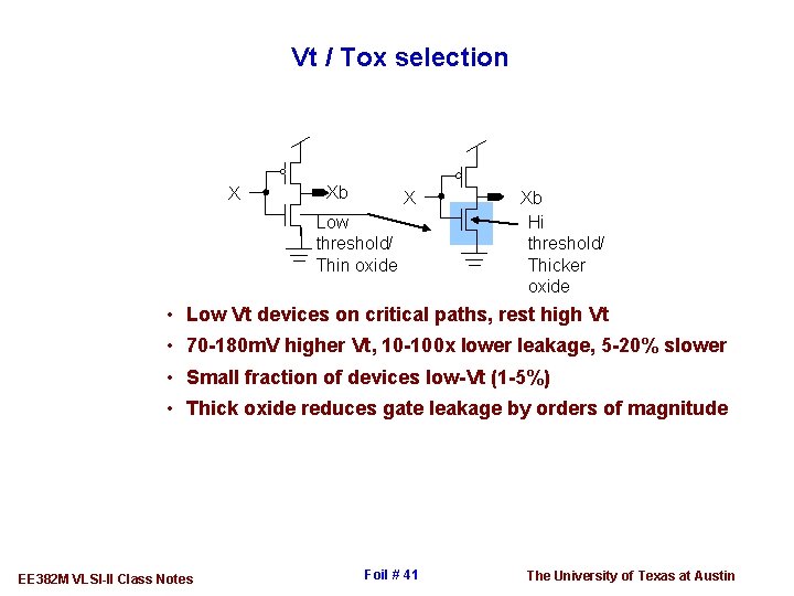
Vt / Tox selection X Xb X Low threshold/ Thin oxide Xb Hi threshold/ Thicker oxide • Low Vt devices on critical paths, rest high Vt • 70 -180 m. V higher Vt, 10 -100 x lower leakage, 5 -20% slower • Small fraction of devices low-Vt (1 -5%) • Thick oxide reduces gate leakage by orders of magnitude EE 382 M VLSI-II Class Notes Foil # 41 The University of Texas at Austin

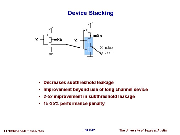
Device Stacking Xb X Stacked devices • Decreases subthreshold leakage • Improvement beyond use of long channel device • 2 -5 x improvement in subthreshold leakage • 15 -35% performance penalty EE 382 M VLSI-II Class Notes Foil # 42 The University of Texas at Austin

Vt or/and Vdd selection • Design tradeoff: – Performance => High supply, low threshold – Active Power => Low supply, low threshold – Standby => Low supply, high threshold • Static – Stack effect – minimizing subthreshold thru single fet paths – Multiple thresholds: High Vt and Low Vt transistors – Multiple supplies: high and low Vdd EE 382 M VLSI-II Class Notes Foil # 43 The University of Texas at Austin

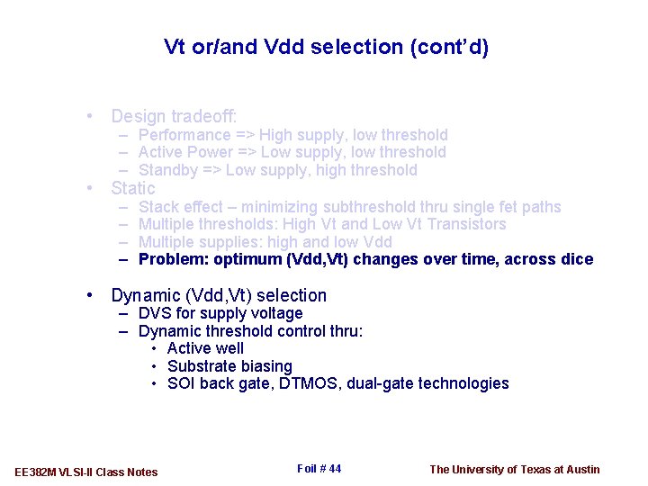
Vt or/and Vdd selection (cont’d) • Design tradeoff: – Performance => High supply, low threshold – Active Power => Low supply, low threshold – Standby => Low supply, high threshold • Static – – Stack effect – minimizing subthreshold thru single fet paths Multiple thresholds: High Vt and Low Vt Transistors Multiple supplies: high and low Vdd Problem: optimum (Vdd, Vt) changes over time, across dice • Dynamic (Vdd, Vt) selection – DVS for supply voltage – Dynamic threshold control thru: • Active well • Substrate biasing • SOI back gate, DTMOS, dual-gate technologies EE 382 M VLSI-II Class Notes Foil # 44 The University of Texas at Austin

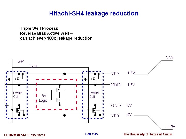
Hitachi-SH 4 leakage reduction Triple Well Process Reverse Bias Active Well – can achieve >100 x leakage reduction 3. 3 V GP GN Switch Cell 1. 8 V Logic Vbp 1. 8 V VDD 1. 8 V GND 0 V Vbn 0 V Switch Cell -1. 5 V EE 382 M VLSI-II Class Notes Foil # 45 The University of Texas at Austin

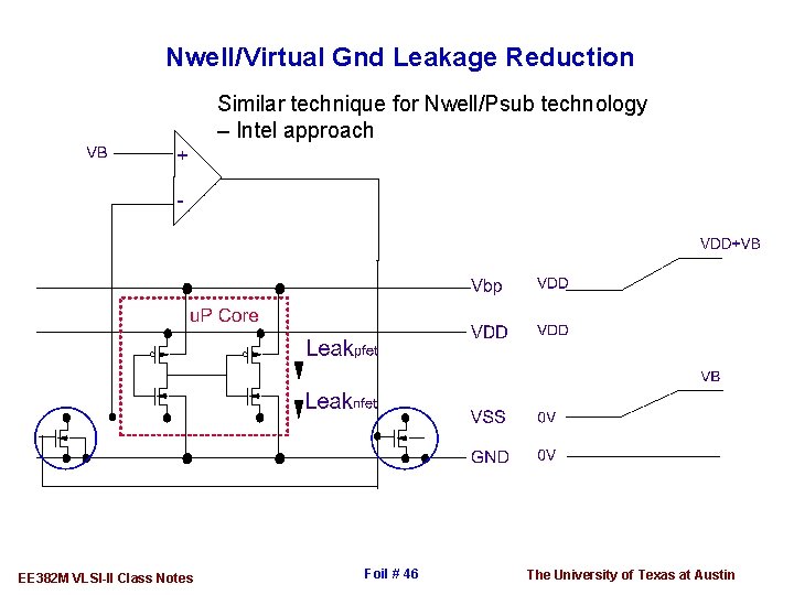
Nwell/Virtual Gnd Leakage Reduction Similar technique for Nwell/Psub technology – Intel approach EE 382 M VLSI-II Class Notes Foil # 46 The University of Texas at Austin

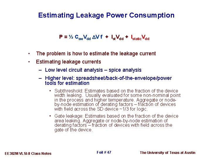
Estimating Leakage Power Consumption P = ½ Csw. Vdd DV f + Ist. Vdd + Istatic. Vdd • The problem is how to estimate the leakage current • Estimating leakage currents – Low level circuit analysis – spice analysis – Higher level: spreadsheet/back-of-the-envelope/power tools for estimation • Subthreshold: Estimates based on the fraction of the device width leaking. Usually evaluated for some non-nominal point in the process and higher temperature. Aggregate or nodeby-node estimation of derating factors – fraction of devices with field across the SD device ~1/3 for logic. • Gate leakage: Estimates based on the fraction of the device area leaking. Aggregate or node-by-node estimation of derating factors – fraction of devices with field across the gate of the device. EE 382 M VLSI-II Class Notes Foil # 47 The University of Texas at Austin

Agenda Overview of VLSI power Technology, Scaling, and Power Review of scaling A look at the real trends and projections for the future Active power – components, trends, managing, estimating Static power – components, trends, managing, estimating Summary EE 382 M VLSI-II Class Notes Foil # 48 The University of Texas at Austin

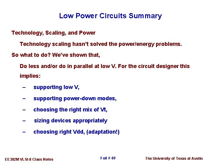
Low Power Circuits Summary Technology, Scaling, and Power Technology scaling hasn’t solved the power/energy problems. So what to do? We’ve shown that, Do less and/or do in parallel at low V. For the circuit designer this implies: – supporting low V, – supporting power-down modes, – choosing the right mix of Vt, – sizing devices appropriately – choosing right Vdd, (adaptation!) EE 382 M VLSI-II Class Notes Foil # 49 The University of Texas at Austin

References • Power Metrics – T. Sakurai and A. Newton, “Alpha-power law MOSFET model and its applications to CMOS inverter delay and other formulas”, IEEE Journal of Solid State Circuits, v. 25. 2, pp. 584 -594, Apr. 1990. – R. Gonzalez, B. Gordon, M. Horowitz, “Supply and threshold voltage scaling for low power CMOS” IEEE Journal of Solid State Circuits, v. 32, no. 8, pp. 1210 -1216, August 2000. – Zyuban and Strenski, “Unified Methodology for Resolving Power. Performance Tradeoffs at the Microarchitectural and Circuit Levels”, ISPLED Aug. 2002 – Brodersen, Horowitz, Markovic, Nikolic, Stojanovic “Methods for True Power Minimization”, ICCAD Nov. 2002 – Stojanovic, Markovic, Nikolic, Horowitz, Brodersen, “Energy-Delay Tradoffs in Combinational Logic using Gate Sizing and Supply Voltage Optimization”, ESSCIRC, Sep. 2002 EE 382 M VLSI-II Class Notes Foil # 50 The University of Texas at Austin

References • Power/Low Power – SIA, International Technology Roadmap for Semiconductors, 2001, 2003, 2005 available online. – V. Agarwal, M. S. Hrishikesh, S. W. Keckler, and D. Burger. "Clock Rate Versus IPC: The End of the Road for Conventional Microarchitectures, " 27 th International Symposium on Computer Architecture (ISCA), June, 2000. – Allan, et. al. , “ 2001 Tech. Roadmap for Semiconductors”, IEEE Computer Jan. 2002 – Chandrakasan, Broderson, (ed) Low Power CMOS Design IEEE Press, 1998. – Oklobdzija (ed) The Computer Engineering Handbook CRC Press, 2002 – Kuo, Lou Low voltage CMOS VLSI Circuits, Wiley, 1999. – Bellaouar, Elmasry, Low Power Digital VLSI Design, Circuits and Systems, Kluwer, 1995. – Chandrakasan, Broderson, Low Power Digital CMOS Design Kluwer, 1995. – A. Correale, “Overview of the power minimization techniques employed in the IBM Power. PC 4 xx embedded controllers” IEEE Symposium on Low Power Electronics Digest of Technical Papers, pp. 75 -80, 1995. – K. Nowka, G. Carpenter, E. Mac. Donald, H. Ngo, B. Brock, K. Ishii, T. Nguyen, J. Burns, “A 0. 9 V to 1. 95 V dynamic voltage scalable and frequency scalable 32 -bit Power. PC processor “, Proceedings of the IEEE International Solid State Circuits Conference, Feb. 2002. – K. Nowka, G. Carpenter, E. Mac. Donald, H. Ngo, B. Brock, K. Ishii, T. Nguyen, J. Burns, “A 32 -bit Power. PC System-on-a-Chip with support for dynamic voltage scaling and dynamic frequency scaling”, IEEE Journal of Solid State Circuits, November, 2002. EE 382 M VLSI-II Class Notes Foil # 51 The University of Texas at Austin

References • Low Voltage / Voltage Scaling – E. Vittoz, “Low-power design: ways to approach the limits” IEEE International Solid State Circuits Conference Digest of Technical Papers, pp. 14 -18, 1994. – M. Horowitz, T. Indermaur, R. Gonzalez, “Low-power digital design” IEEE Symposium on Low Power Electronics Digest of Technical Papers, pp. 8 -11, 1994. – R. Gonzalez, B. Gordon, M. Horowitz, “Supply and threshold voltage scaling for low power CMOS” IEEE Journal of Solid State Circuits, v. 32, no. 8, pp. 1210 -1216, August 2000. – T. Burd and R. Brodersen, “Energy efficient CMOS microprocessor design ” Proceedings of the Twenty-Eighth Hawaii International Conference on System Sciences, v. 1, pp. 288 -297, 466, 1995. – K. Suzuki, S. Mita, T. Fujita, F. Yamane, F. Sano, A. Chiba, Y. Watanabe, K. Matsuda, T. Maeda, T. Kuroda, “A 300 MIPS/W RISC core processor with variable supply-voltage scheme in variable threshold-voltage CMOS” Proceedings of the IEEE Conference on Custom Integrated Circuits Conference, pp. 587 – 590, 1997 – T. Kuroda, K. Suzuki, S. Mita, T. Fujita, F. Yamane, F. Sano, A. Chiba, Y. Watanabe, K. Matsuda, T. Maeda, T. Sakurai, T. Furuyama, “Variable supply-voltage scheme for lowpower high-speed CMOS digital design” IEEE Journal of Solid State Circuits, v. 33, no. 3, pp. 454 -462, March 1998. – T. Burd, T. Pering, A. Stratakos, R. Brodersen, “A dynamic voltage scaled microprocessor system ” IEEE International Solid State Circuits Conference Digest of Technical Papers, pp. 294 -295, 466, 2000. EE 382 M VLSI-II Class Notes Foil # 52 The University of Texas at Austin

References • Technology and Circuit Techniques – E. Nowak, et al. , “Scaling beyond the 65 nm node with Fin. FET-DGCMOS” Proceedings of the IEEE Custom Integrated Circuits Conference, Sept. 21 -24, 2003, pp. 339 – 342 – L. Clark, et al. “An embedded 32 b microprocessor core for low-power and highperformnace applications”, IEEE Journal of Solid State Circuits, V. 36, No. 11, Nov. 2001, pp. 1599 -1608 – S. Mukhopadhyay, C. Neau, R. Cakici, A. Agarwal, C. Kim, and K. Roy, “Gate leakage reduction for scaled devices using transistor stacking” IEEE Transactions on Very Large Scale Integration (VLSI) Systems, Aug. 2003, pp. 716 – 730 – A. Bhavnagarwala, et al. , “A pico-joule class, 1 GHz, 32 Kbyte x 64 b DSP SRAM with Self Reverse Bias” 2003 Symposium on VLSI Circuits, June 2003, pp. 251 -251. – S. Mutoh, et al. , “ 1 -V Power Supply High-Speed Digital Circuit Technology with Multi. Threshold Voltage CMOS, ” IEEE Journal of Solid State Circuits, vol. 30, no. 8, pp. 847854, 1995. – K. Das, et al. , “New Optimal Design Strategies and Analysis of Ultra-Low Leakage Circuits for Nano- Scale SOI Technology, ” Proc. ISLPED, pp. 168 -171, 2003. – R. Rao, J. Burns and R. Brown, “Circuit Techniques for Gate and Sub-Threshold Leakage Minimization in Future CMOS Technologies” Proc. ESSCIRC, pp. 2790 -2795, 2003. – R. Rao, J. Burns and R. Brown, “Analysis and optimization of enhanced MTCMOS scheme” Proc. 17 th International Conference on VLSI Design, 2004, pp. 234 -239. EE 382 M VLSI-II Class Notes Foil # 53 The University of Texas at Austin