EE 5324 VLSI Design II Part VI Testing
![Why Testing? • If you don’t test it, it won’t work! (guaranteed) [WE 992] Why Testing? • If you don’t test it, it won’t work! (guaranteed) [WE 992]](https://slidetodoc.com/presentation_image/fd106e474120c07b9356baaa9d7b60bc/image-2.jpg)

![Scan-Based Testing on Pipelined Designs • Efficient: use the existing registers A B REG[1] Scan-Based Testing on Pipelined Designs • Efficient: use the existing registers A B REG[1]](https://slidetodoc.com/presentation_image/fd106e474120c07b9356baaa9d7b60bc/image-24.jpg)
- Slides: 35

EE 5324 – VLSI Design II Part VI: Testing Kia Bazargan University of Minnesota Spring 2006 EE 5324 - VLSI Design II - © Kia Bazargan 264
![Why Testing If you dont test it it wont work guaranteed WE 992 Why Testing? • If you don’t test it, it won’t work! (guaranteed) [WE 992]](https://slidetodoc.com/presentation_image/fd106e474120c07b9356baaa9d7b60bc/image-2.jpg)
Why Testing? • If you don’t test it, it won’t work! (guaranteed) [WE 992] • Intel’s Pentium division bug (’ 94 -’ 95) • Intel’s top ten slogans for Pentium: [ Oxford] Ø 9. 999997325 Ø 8. 999916336 Ø 7. 999941461 Ø 6. 999983153 It’s a FLAW, dammit, not a bug Redefining the PC – and math Nearly 300 correct opcodes Why do you think it’s called “floating” point? Ø. . . • Taking more and more of design cycle time • Have to plan for testing when designing Spring 2006 EE 5324 - VLSI Design II - © Kia Bazargan 265

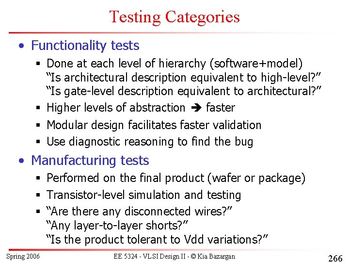
Testing Categories • Functionality tests § Done at each level of hierarchy (software+model) “Is architectural description equivalent to high-level? ” “Is gate-level description equivalent to architectural? ” § Higher levels of abstraction faster § Modular design facilitates faster validation § Use diagnostic reasoning to find the bug • Manufacturing tests § Performed on the final product (wafer or package) § Transistor-level simulation and testing § “Are there any disconnected wires? ” “Any layer-to-layer shorts? ” “Is the product tolerant to Vdd variations? ” Spring 2006 EE 5324 - VLSI Design II - © Kia Bazargan 266

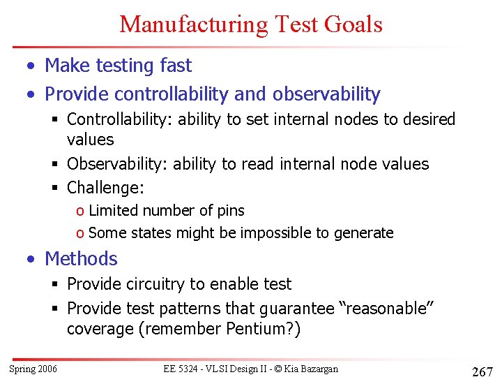
Manufacturing Test Goals • Make testing fast • Provide controllability and observability § Controllability: ability to set internal nodes to desired values § Observability: ability to read internal node values § Challenge: o Limited number of pins o Some states might be impossible to generate • Methods § Provide circuitry to enable test § Provide test patterns that guarantee “reasonable” coverage (remember Pentium? ) Spring 2006 EE 5324 - VLSI Design II - © Kia Bazargan 267

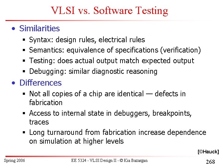
VLSI vs. Software Testing • Similarities § § Syntax: design rules, electrical rules Semantics: equivalence of specifications (verification) Testing: does actual output match expected output Debugging: similar diagnostic reasoning • Differences § Not all copies of a chip are identical — defects in fabrication § Access to internal state in debuggers, breakpoints, traces § Long turnaround from fabrication increase dependence on simulation at higher levels [©Hauck] Spring 2006 EE 5324 - VLSI Design II - © Kia Bazargan 268

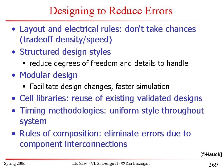
Designing to Reduce Errors • Layout and electrical rules: don't take chances (tradeoff density/speed) • Structured design styles § reduce degrees of freedom and details to handle • Modular design § Facilitate design changes, faster simulation • Cell libraries: reuse of existing validated designs • Timing methodologies: uniform style throughout system • Rules of composition: eliminate errors due to component interconnections [©Hauck] Spring 2006 EE 5324 - VLSI Design II - © Kia Bazargan 269

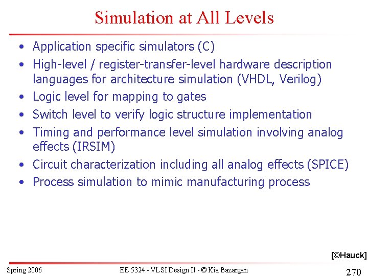
Simulation at All Levels • Application specific simulators (C) • High-level / register-transfer-level hardware description languages for architecture simulation (VHDL, Verilog) • Logic level for mapping to gates • Switch level to verify logic structure implementation • Timing and performance level simulation involving analog effects (IRSIM) • Circuit characterization including all analog effects (SPICE) • Process simulation to mimic manufacturing process [©Hauck] Spring 2006 EE 5324 - VLSI Design II - © Kia Bazargan 270

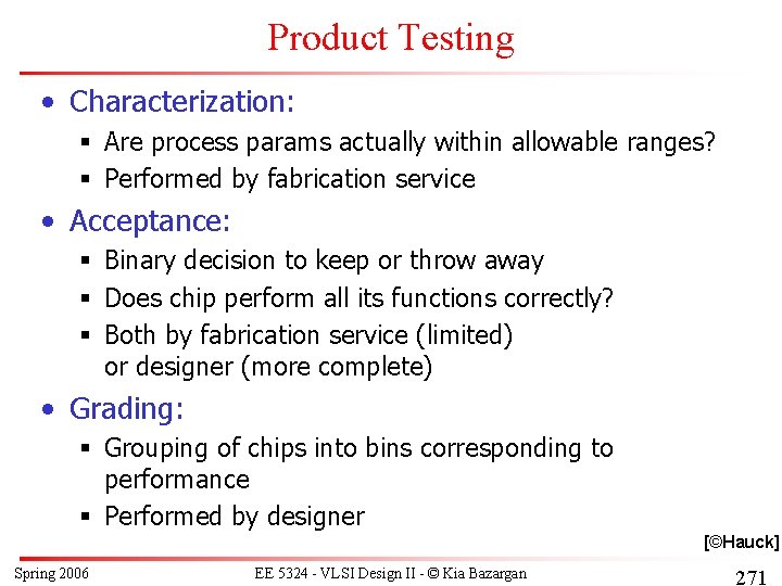
Product Testing • Characterization: § Are process params actually within allowable ranges? § Performed by fabrication service • Acceptance: § Binary decision to keep or throw away § Does chip perform all its functions correctly? § Both by fabrication service (limited) or designer (more complete) • Grading: § Grouping of chips into bins corresponding to performance § Performed by designer [©Hauck] Spring 2006 EE 5324 - VLSI Design II - © Kia Bazargan 271

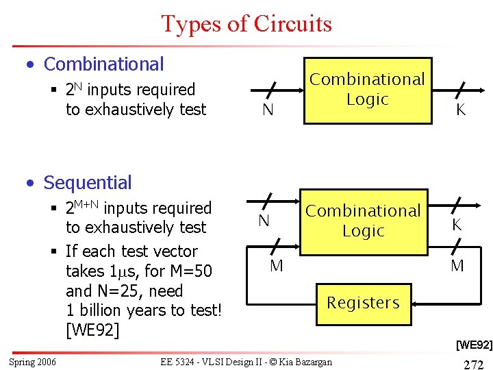
Types of Circuits • Combinational § 2 N inputs required to exhaustively test N Combinational Logic K • Sequential § 2 M+N inputs required to exhaustively test § If each test vector takes 1 ms, for M=50 and N=25, need 1 billion years to test! [WE 92] Spring 2006 N Combinational Logic M K M Registers EE 5324 - VLSI Design II - © Kia Bazargan [WE 92] 272

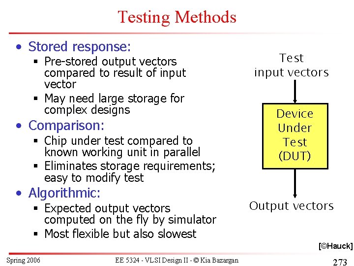
Testing Methods • Stored response: § Pre-stored output vectors compared to result of input vector § May need large storage for complex designs • Comparison: § Chip under test compared to known working unit in parallel § Eliminates storage requirements; easy to modify test • Algorithmic: § Expected output vectors computed on the fly by simulator § Most flexible but also slowest Test input vectors Device Under Test (DUT) Output vectors [©Hauck] Spring 2006 EE 5324 - VLSI Design II - © Kia Bazargan 273

Generating and Validating Test Vectors • Automatic test-pattern generation (ATPG) § For given fault, determine test (aka excitation) vector that will propagate error to observable output § Most available tools: combinational networks only • Fault simulation § Determine minimal test vectors that will sensitize circuit to the fault § Simulates correct network in parallel with faulty networks § Structure of logic may make some faults untestable • Both require adequate models of faults in CMOS integrated circuits [©Hauck] [©Prentice Hall] Spring 2006 EE 5324 - VLSI Design II - © Kia Bazargan 274

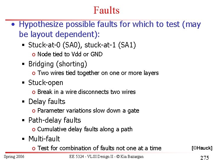
Faults • Hypothesize possible faults for which to test (may be layout dependent): § Stuck-at-0 (SA 0), stuck-at-1 (SA 1) o Node tied to Vdd or GND § Bridging (shorting) o Two wires tied together on one or more layers § Stuck-open o Break in a wire disconnects two wires § Delay faults o Parameter variations slow down a gate § Path-delay faults o Cumulative delay faults along a path § Multi-fault o Test for combination of faults not one at a time Spring 2006 EE 5324 - VLSI Design II - © Kia Bazargan [©Hauck] 275

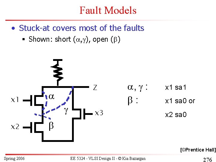
Fault Models • Stuck-at covers most of the faults § Shown: short (a, g), open (b) x 1 x 2 Z a g a, g : b: x 3 x 1 sa 1 x 1 sa 0 or x 2 sa 0 b [©Prentice Hall] Spring 2006 EE 5324 - VLSI Design II - © Kia Bazargan 276

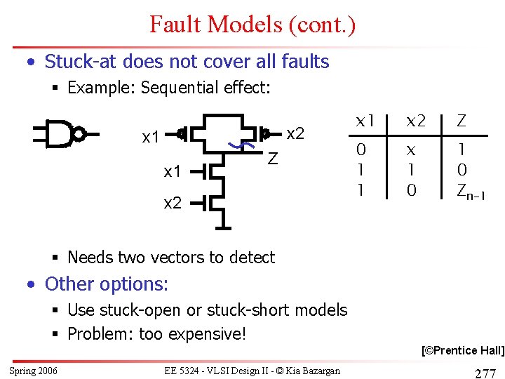
Fault Models (cont. ) • Stuck-at does not cover all faults § Example: Sequential effect: x 2 x 1 Z x 2 x 1 x 2 Z 0 1 1 x 1 0 Zn-1 § Needs two vectors to detect • Other options: § Use stuck-open or stuck-short models § Problem: too expensive! [©Prentice Hall] Spring 2006 EE 5324 - VLSI Design II - © Kia Bazargan 277

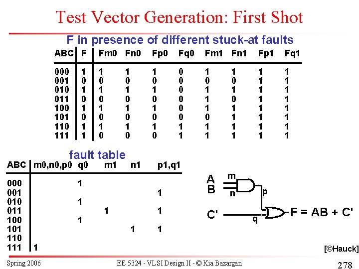
Test Vector Generation: First Shot F in presence of different stuck-at faults ABC F Fm 0 Fn 0 Fp 0 Fq 0 Fm 1 Fn 1 Fp 1 Fq 1 000 001 010 011 100 101 110 111 1 0 1 0 0 0 0 1 1 1 1 1 1 1 0 1 0 1 1 1 0 1 0 fault table ABC m 0, n 0, p 0 q 0 001 010 011 100 101 110 111 m 1 n 1 1 p 1, q 1 1 1 0 1 1 1 1 A B m C' q F = AB + C' 1 1 Spring 2006 p n [©Hauck] EE 5324 - VLSI Design II - © Kia Bazargan 278

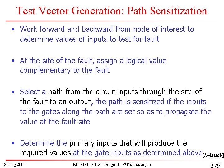
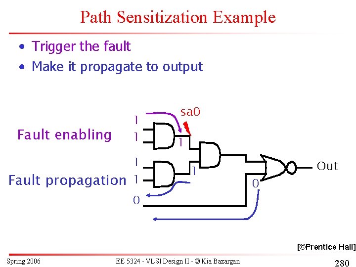
Test Vector Generation: Path Sensitization • Work forward and backward from node of interest to determine values of inputs to test for fault • At the site of the fault, assign a logical value complementary to the fault • Select a path from the circuit inputs through the site of the fault to an output, the path is sensitized if the inputs to the gates along the path are set so as to propagate the value at the fault site • Determine the primary inputs that will produce the required values at the gate inputs as determined above[©Hauck] Spring 2006 EE 5324 - VLSI Design II - © Kia Bazargan 279

Path Sensitization Example • Trigger the fault • Make it propagate to output Fault enabling 1 1 1 Fault propagation 1 sa 0 1 1 0 0 Out [©Prentice Hall] Spring 2006 EE 5324 - VLSI Design II - © Kia Bazargan 280

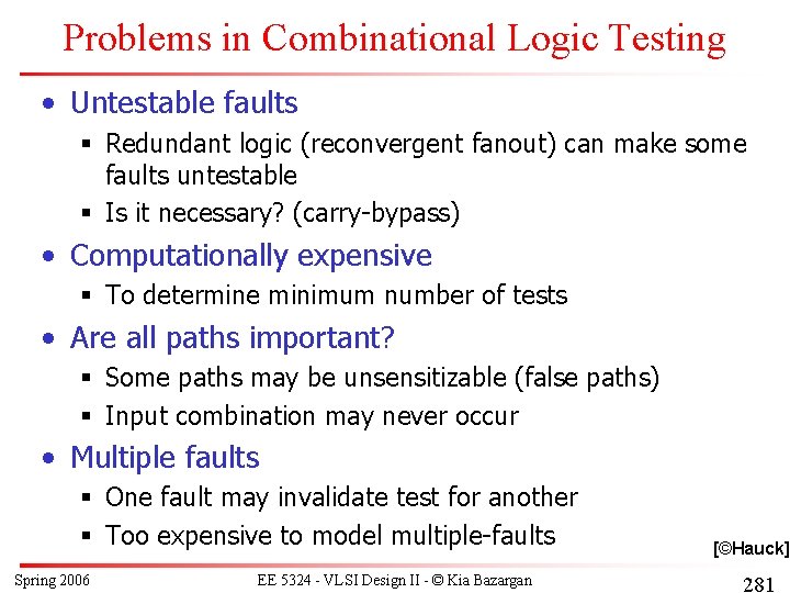
Problems in Combinational Logic Testing • Untestable faults § Redundant logic (reconvergent fanout) can make some faults untestable § Is it necessary? (carry-bypass) • Computationally expensive § To determine minimum number of tests • Are all paths important? § Some paths may be unsensitizable (false paths) § Input combination may never occur • Multiple faults § One fault may invalidate test for another § Too expensive to model multiple-faults Spring 2006 EE 5324 - VLSI Design II - © Kia Bazargan [©Hauck] 281

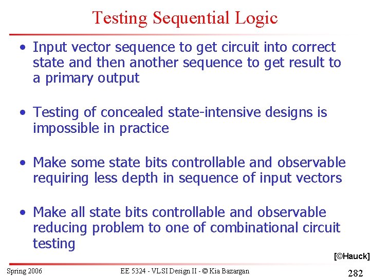
Testing Sequential Logic • Input vector sequence to get circuit into correct state and then another sequence to get result to a primary output • Testing of concealed state-intensive designs is impossible in practice • Make some state bits controllable and observable requiring less depth in sequence of input vectors • Make all state bits controllable and observable reducing problem to one of combinational circuit testing [©Hauck] Spring 2006 EE 5324 - VLSI Design II - © Kia Bazargan 282

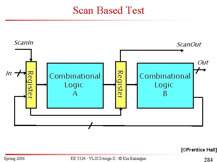
Level Sensitive Scan Design (LSSD) • Known as scan-based test • Scan path (shift register) links all state elements in circuit • Observe and control all states • Requires 3 extra pins and a bit more logic in FFs • All tests become combinational • Very slow — shift in test vector and shift output vector serially — partial scan paths only use necessary amount • Easy to extend to system level [©Hauck] Spring 2006 EE 5324 - VLSI Design II - © Kia Bazargan 283

Scan Based Test Scan. In Scan. Out Combinational Logic A Register In Combinational Logic B [©Prentice Hall] Spring 2006 EE 5324 - VLSI Design II - © Kia Bazargan 284

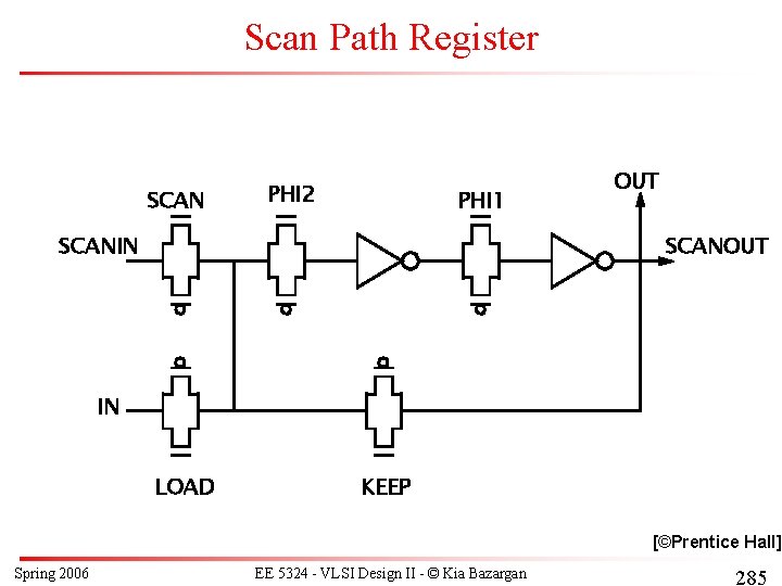
Scan Path Register SCAN PHI 2 PHI 1 SCANIN OUT SCANOUT IN LOAD KEEP [©Prentice Hall] Spring 2006 EE 5324 - VLSI Design II - © Kia Bazargan 285

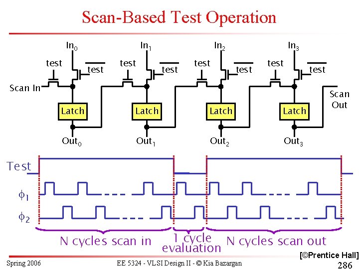
Scan-Based Test Operation In 0 test In 1 test In 2 test In 3 test Scan In Latch Out 0 Out 1 Out 2 Out 3 Scan Out Test f 1 f 2 N cycles scan in Spring 2006 1 cycle N cycles scan out evaluation EE 5324 - VLSI Design II - © Kia Bazargan [©Prentice Hall] 286
![ScanBased Testing on Pipelined Designs Efficient use the existing registers A B REG1 Scan-Based Testing on Pipelined Designs • Efficient: use the existing registers A B REG[1]](https://slidetodoc.com/presentation_image/fd106e474120c07b9356baaa9d7b60bc/image-24.jpg)
Scan-Based Testing on Pipelined Designs • Efficient: use the existing registers A B REG[1] REG[0] REG[2] REG[3] SCANIN + REG[4] COMPIN COMP REG[5] SCANOUT Spring 2006 EE 5324 - VLSI Design II - © Kia Bazargan [©Prentice Hall] 287

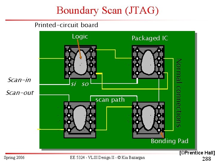
Boundary Scan (JTAG) Printed-circuit board Logic Scan-out si so scan path N o r m a l c o n n e c ti o n s Scan-in Packaged IC Bonding Pad Spring 2006 EE 5324 - VLSI Design II - © Kia Bazargan [©Prentice Hall] 288

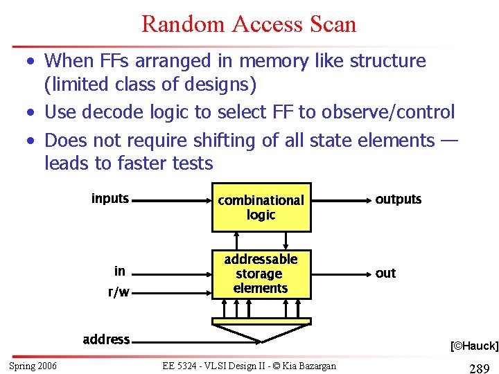
Random Access Scan • When FFs arranged in memory like structure (limited class of designs) • Use decode logic to select FF to observe/control • Does not require shifting of all state elements — leads to faster tests inputs in r/w combinational logic addressable storage elements address Spring 2006 outputs out [©Hauck] EE 5324 - VLSI Design II - © Kia Bazargan 289

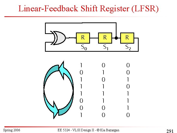
Self Testing • Built-in self test (BIST) • Chip itself generates test vectors (internally) § Dedicated sub-circuit to generate pseudo-random test vectors § Use “linear feedback shift register (LFSR)” to generate test vectors • Use signature to check the integrity § Apply sequences of input vectors and combine the output into a signature • Shift in initial seed and shift out the signature Spring 2006 EE 5324 - VLSI Design II - © Kia Bazargan 290

Linear-Feedback Shift Register (LFSR) Spring 2006 R R R S 0 S 1 S 2 1 0 1 1 1 0 0 1 0 1 1 1 0 EE 5324 - VLSI Design II - © Kia Bazargan 291

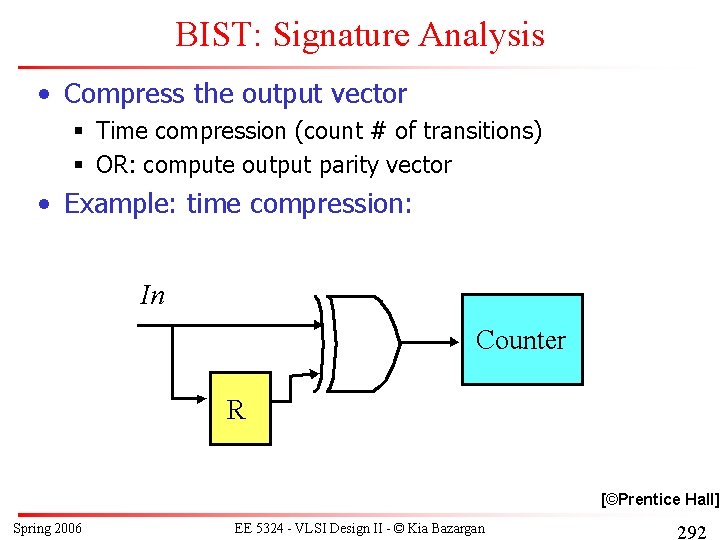
BIST: Signature Analysis • Compress the output vector § Time compression (count # of transitions) § OR: compute output parity vector • Example: time compression: In Counter R [©Prentice Hall] Spring 2006 EE 5324 - VLSI Design II - © Kia Bazargan 292

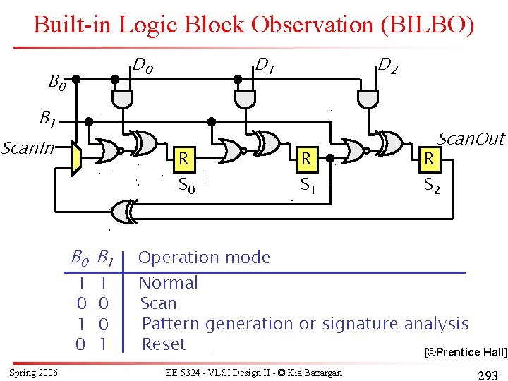
Built-in Logic Block Observation (BILBO) D 0 B 0 D 1 D 2 B 1 Scan. In R S 0 B 1 1 0 Spring 2006 1 0 0 1 R Scan. Out S 2 Operation mode Normal Scan Pattern generation or signature analysis Reset [©Prentice Hall] EE 5324 - VLSI Design II - © Kia Bazargan 293

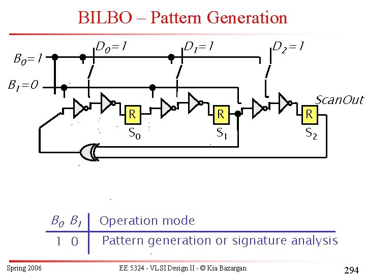
BILBO – Pattern Generation D 0 =1 B 0=1 D 1=1 D 2 =1 B 1=0 Scan. In R S 0 B 1 1 0 Spring 2006 R S 1 R Scan. Out S 2 Operation mode Pattern generation or signature analysis EE 5324 - VLSI Design II - © Kia Bazargan 294

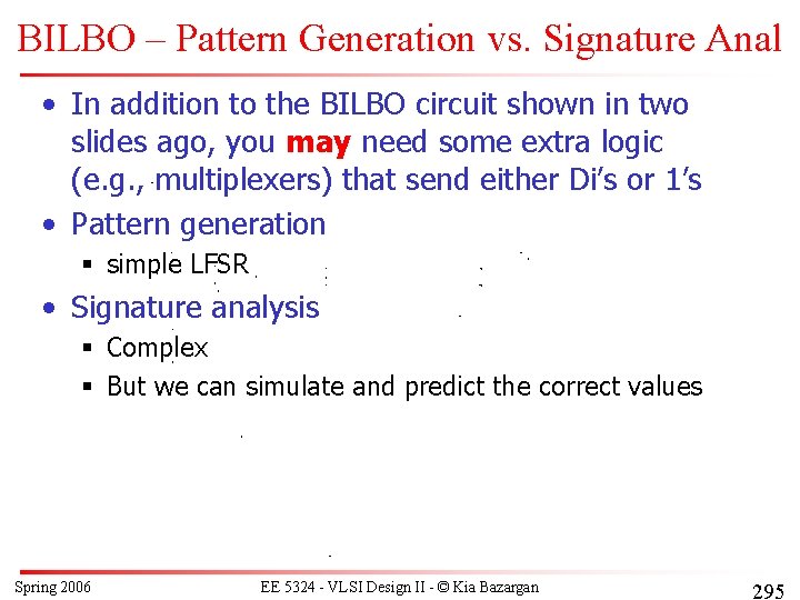
BILBO – Pattern Generation vs. Signature Anal • In addition to the BILBO circuit shown in two slides ago, you may need some extra logic (e. g. , multiplexers) that send either Di’s or 1’s • Pattern generation § simple LFSR • Signature analysis § Complex § But we can simulate and predict the correct values Spring 2006 EE 5324 - VLSI Design II - © Kia Bazargan 295

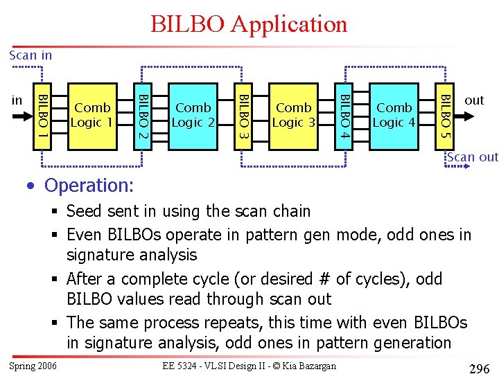
BILBO Application Scan in Comb Logic 4 BILBO 5 Comb Logic 3 BILBO 4 Comb Logic 2 BILBO 3 Comb Logic 1 BILBO 2 BILBO 1 in out Scan out • Operation: § Seed sent in using the scan chain § Even BILBOs operate in pattern gen mode, odd ones in signature analysis § After a complete cycle (or desired # of cycles), odd BILBO values read through scan out § The same process repeats, this time with even BILBOs in signature analysis, odd ones in pattern generation Spring 2006 EE 5324 - VLSI Design II - © Kia Bazargan 296

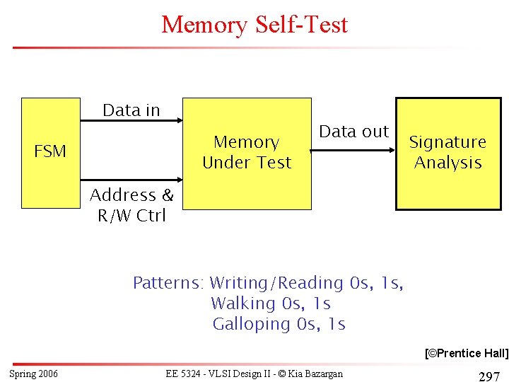
Memory Self-Test Data in Memory Under Test FSM Data out Signature Analysis Address & R/W Ctrl Patterns: Writing/Reading 0 s, 1 s, Walking 0 s, 1 s Galloping 0 s, 1 s [©Prentice Hall] Spring 2006 EE 5324 - VLSI Design II - © Kia Bazargan 297

To Probe Further (Testing) • BIST § K. A. Ockunzzi and C. Papachristou, "Test Strategies for BIST at the Algorithmic and Register-Transfer Levels", Design Automation Conference, pp. 65 -70, 2001. • LFSR § W. G. Solomon, “Shift Register Sequences”, Aegean Park Press, 1982. Spring 2006 EE 5324 - VLSI Design II - © Kia Bazargan 298