EE 466 VLSI Design CAMs ROMs and PLAs
- Slides: 17

EE 466: VLSI Design CAMs, ROMs, and PLAs 14: CAMs, ROMs, and PLAs 1

Outline q Content-Addressable Memories q Read-Only Memories q Programmable Logic Arrays 14: CAMs, ROMs, and PLAs CMOS VLSI Design 2

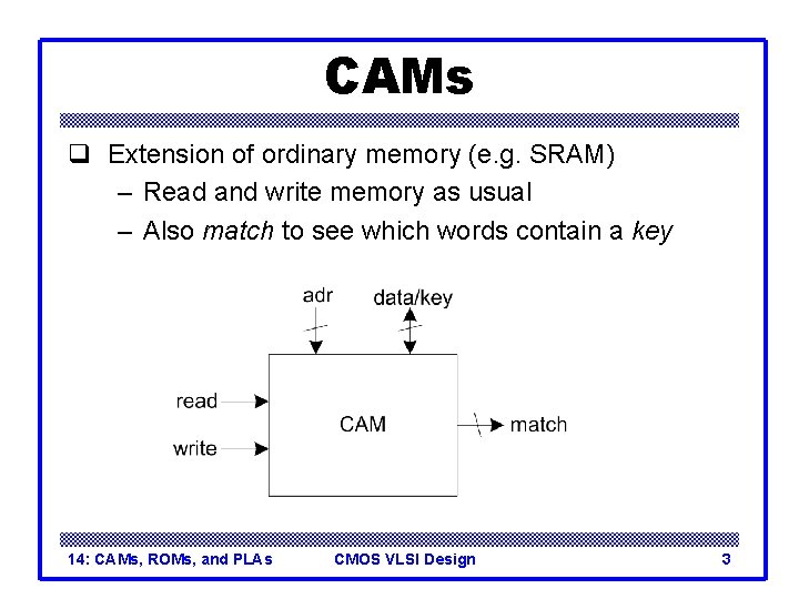
CAMs q Extension of ordinary memory (e. g. SRAM) – Read and write memory as usual – Also match to see which words contain a key 14: CAMs, ROMs, and PLAs CMOS VLSI Design 3

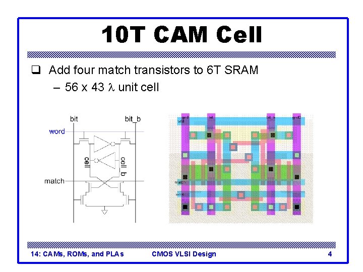
10 T CAM Cell q Add four match transistors to 6 T SRAM – 56 x 43 l unit cell 14: CAMs, ROMs, and PLAs CMOS VLSI Design 4

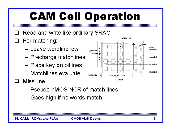
CAM Cell Operation q Read and write like ordinary SRAM q For matching: – Leave wordline low – Precharge matchlines – Place key on bitlines – Matchlines evaluate q Miss line – Pseudo-n. MOS NOR of match lines – Goes high if no words match 14: CAMs, ROMs, and PLAs CMOS VLSI Design 5

Read-Only Memories q Read-Only Memories are nonvolatile – Retain their contents when power is removed q Mask-programmed ROMs use one transistor per bit – Presence or absence determines 1 or 0 14: CAMs, ROMs, and PLAs CMOS VLSI Design 6

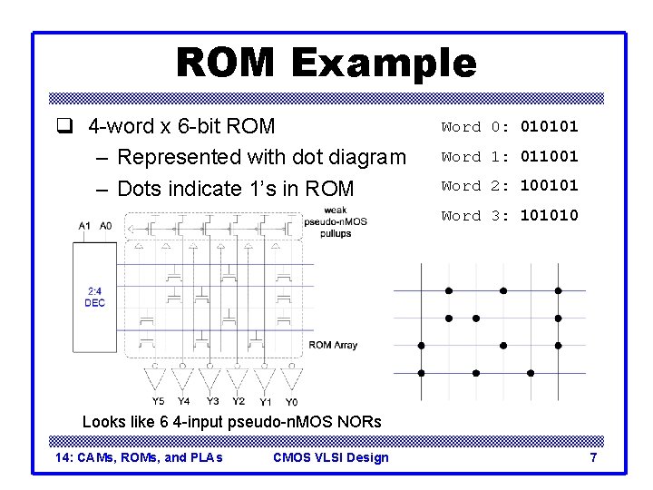
ROM Example q 4 -word x 6 -bit ROM – Represented with dot diagram – Dots indicate 1’s in ROM Word 0: 010101 Word 1: 011001 Word 2: 100101 Word 3: 101010 Looks like 6 4 -input pseudo-n. MOS NORs 14: CAMs, ROMs, and PLAs CMOS VLSI Design 7

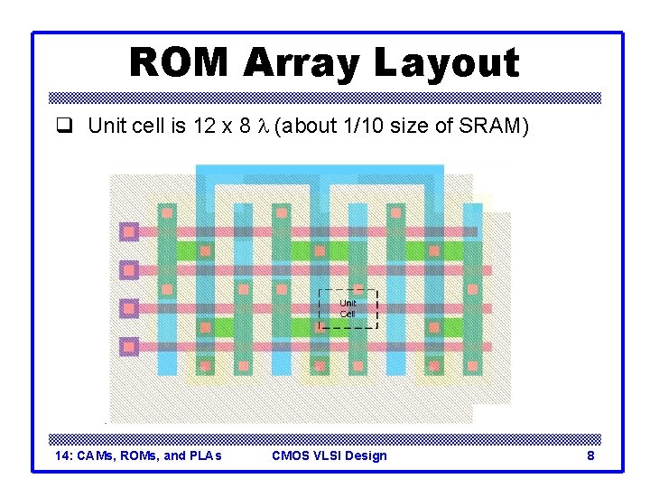
ROM Array Layout q Unit cell is 12 x 8 l (about 1/10 size of SRAM) 14: CAMs, ROMs, and PLAs CMOS VLSI Design 8

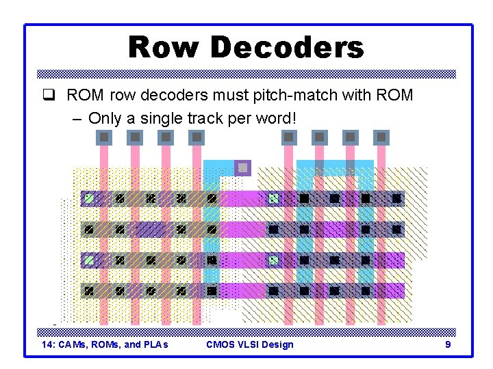
Row Decoders q ROM row decoders must pitch-match with ROM – Only a single track per word! 14: CAMs, ROMs, and PLAs CMOS VLSI Design 9

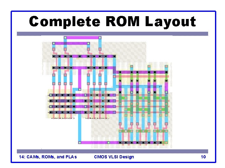
Complete ROM Layout 14: CAMs, ROMs, and PLAs CMOS VLSI Design 10

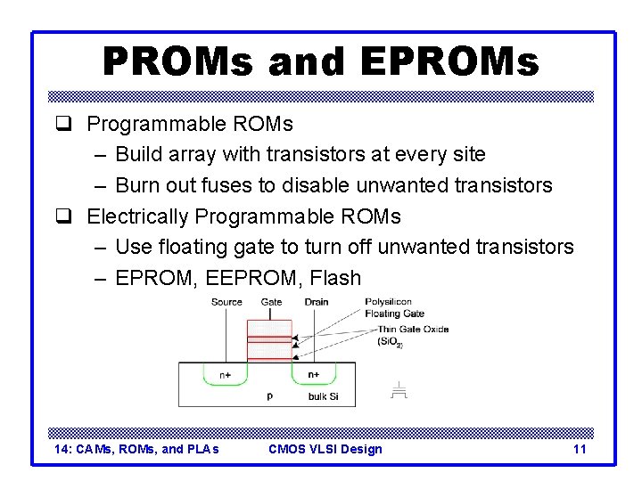
PROMs and EPROMs q Programmable ROMs – Build array with transistors at every site – Burn out fuses to disable unwanted transistors q Electrically Programmable ROMs – Use floating gate to turn off unwanted transistors – EPROM, EEPROM, Flash 14: CAMs, ROMs, and PLAs CMOS VLSI Design 11

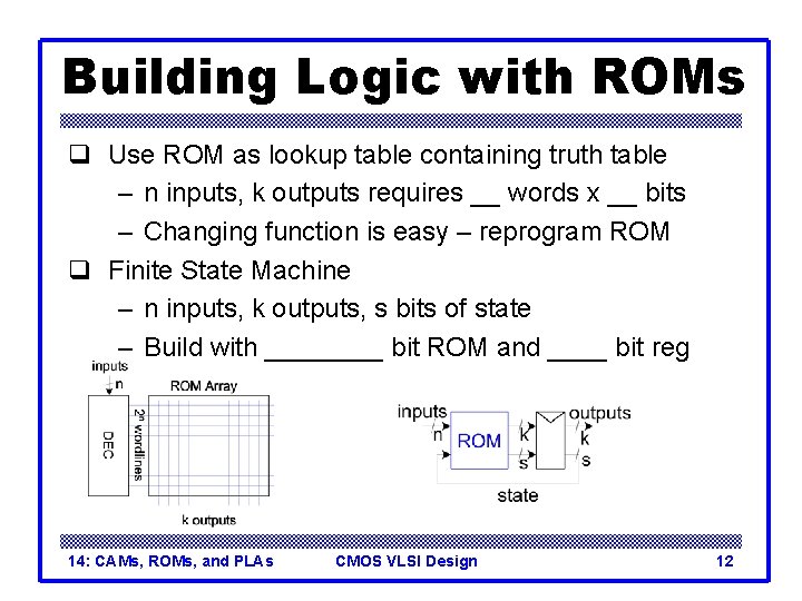
Building Logic with ROMs q Use ROM as lookup table containing truth table – n inputs, k outputs requires __ words x __ bits – Changing function is easy – reprogram ROM q Finite State Machine – n inputs, k outputs, s bits of state – Build with ____ bit ROM and ____ bit reg 14: CAMs, ROMs, and PLAs CMOS VLSI Design 12

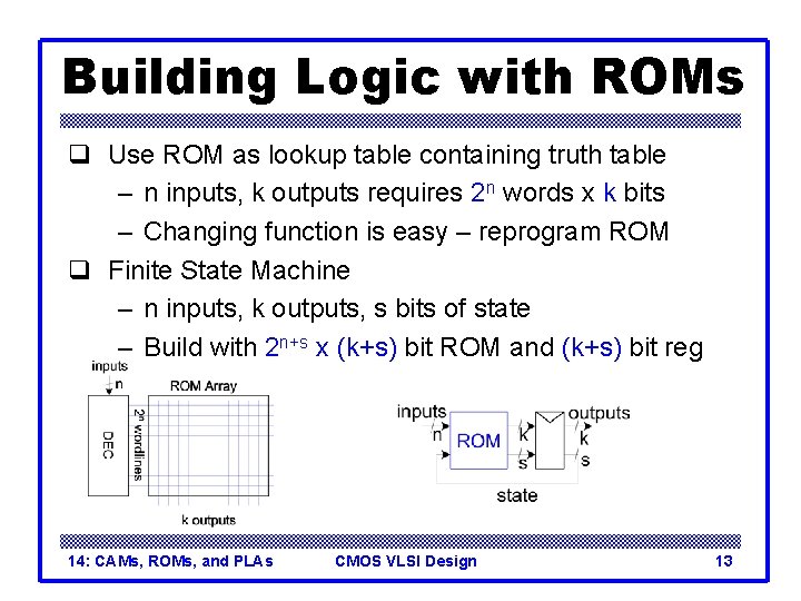
Building Logic with ROMs q Use ROM as lookup table containing truth table – n inputs, k outputs requires 2 n words x k bits – Changing function is easy – reprogram ROM q Finite State Machine – n inputs, k outputs, s bits of state – Build with 2 n+s x (k+s) bit ROM and (k+s) bit reg 14: CAMs, ROMs, and PLAs CMOS VLSI Design 13

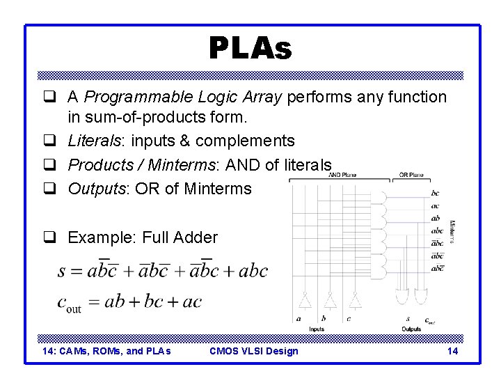
PLAs q A Programmable Logic Array performs any function in sum-of-products form. q Literals: inputs & complements q Products / Minterms: AND of literals q Outputs: OR of Minterms q Example: Full Adder 14: CAMs, ROMs, and PLAs CMOS VLSI Design 14

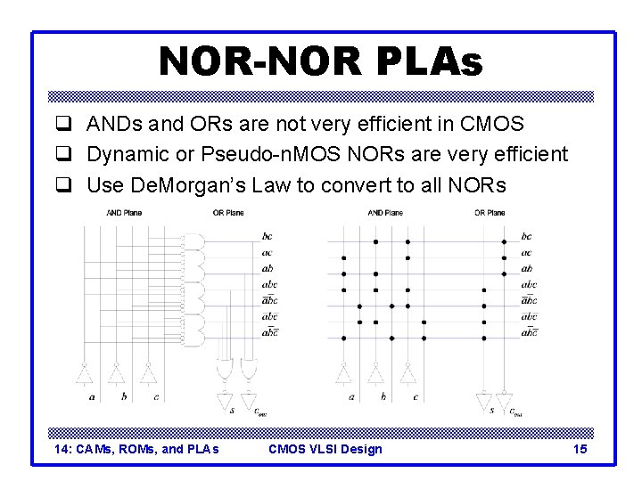
NOR-NOR PLAs q ANDs and ORs are not very efficient in CMOS q Dynamic or Pseudo-n. MOS NORs are very efficient q Use De. Morgan’s Law to convert to all NORs 14: CAMs, ROMs, and PLAs CMOS VLSI Design 15

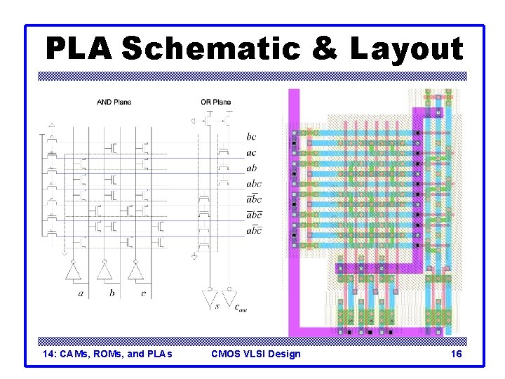
PLA Schematic & Layout 14: CAMs, ROMs, and PLAs CMOS VLSI Design 16

PLAs vs. ROMs q The OR plane of the PLA is like the ROM array q The AND plane of the PLA is like the ROM decoder q PLAs are more flexible than ROMs – No need to have 2 n rows for n inputs – Only generate the minterms that are needed – Take advantage of logic simplification 14: CAMs, ROMs, and PLAs CMOS VLSI Design 17