EE 4611 INTRODUCTION 21 January 2015 Semiconductor Industry


- Slides: 9
EE 4611 INTRODUCTION 21 January 2015 Semiconductor Industry Milestones • 1942 - Very pure silicon and germanium were manufactured • 1947 - PN junction diodes was invented • 1947 - The junction transistor was invented at Bell Lab by Bardeen, Brattain and Schockley • 1958 - Integrated circuits (ICs) were invented by Kilby at TI • 1962 - First commercial integrated circuits • 1962 - Semiconductor industry surpasses $1 -billion in sales • 1963 - First MOS IC • 1963 - CMOS invented • 1965 - Moore’s law invented by Intel co-founder Gordon E. Moore • 1971 - Microprocessor invented • 1978 - Semiconductor Industry passes $10 -billion. • 1985 - Intel 80386 DX • 1985 - 200 mm silicon wafers introduced • 1986 - 1 Mbit DRAM • 1988 - 4 Mbit DRAM • 1989 - Intel 80486 DXTM • 1990’s-2000’s Intel Pentium Series • 2009 - Intel demonstrated the first working 32 nm processor • 2012 – Micron 22 nm memory 1
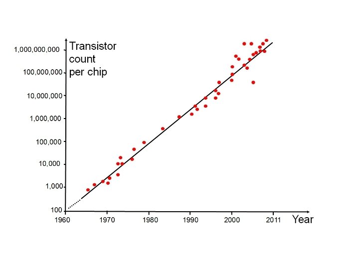
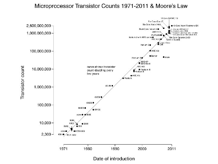
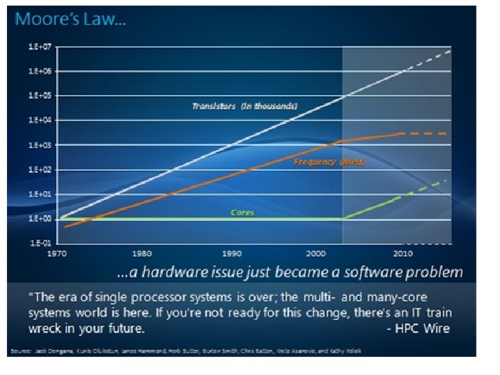
Moore’s Law • Number of transistors on a chip roughly double every 18 months • Has been true since 1970 and shows no signs of slowing • World's first 2 -billion transistor microprocessor (Intel Itanium processor) is announced in February 2008 2
Device Becomes Ever Smaller • Smaller feather size leads to more transistors per unit area (high density) and higher speed • Intel demonstrated the first working 32 nm processor in 2009 • 2012 feature sizes 22 nm, advanced R&D to 14 nm • January 2013 IEEE Spectrum 3 -D “Fin. FET” R&D by INTEL and others 3
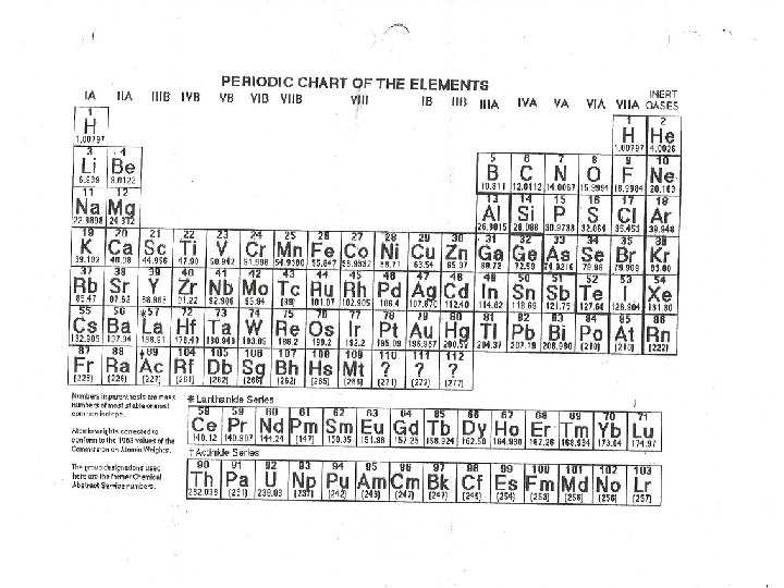
Semiconductor Materials • Elements: Si, Ge • III-V compounds: Al. As, Ga. As, In. P • II-VI compounds: Cd. S, Cd. Se, Zn. S, • Si is today’s most important semiconductor material ― Low cost ― easily oxidized to form Si. O 2 insulating layer ― High Eg, can be used in high temperature Periodic table of semiconductors • Ga. As and In. P are used for optoelectronic applications 8
Semiconductor Industry Development Trend: smaller, faster, and cheaper Ways to achieve: • Better quality of fabrication materials, e. g. , very pure semiconductors and large single crystals • New materials (such as graphene, carbon nano tube) • New design concepts and new theories on semiconductor physics • New fabrication technology • Micro- and nano- technology • Energy efficient devices • New theory 9