EE 434 Lecture 12 Devices in Semiconductor Processes




- Slides: 35

EE 434 Lecture 12 Devices in Semiconductor Processes Diodes Capacitors MOS Transistors

Quiz 10 A “ 10 K” resistor has a temperature coefficient of +80 ppm/o. C If the resistor was measured to be 9. 83 K at 20 o. C, what would be the resistor value at 80 o. C?

And the number is ….

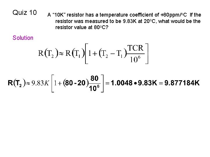
Quiz 10 Solution A “ 10 K” resistor has a temperature coefficient of +80 ppm/o. C If the resistor was measured to be 9. 83 K at 20 o. C, what would be the resistor value at 80 o. C?

Review from Last Time • Process Flow is a “recipe” for the process – Shows what can and can not be made – Gives insight into performance capabilities and limitations • Back-End Processes – Die attach options (eutectic, preform, conductive epoxy) • Stresses the die – Bonding • Wire bonding • Bump bonding – Packaging • Many packaging options • Package Costs can be large so defective die should be eliminated before packaging

Basic Devices and Device Models • • • Resistor Diode Capacitor MOSFET BJT

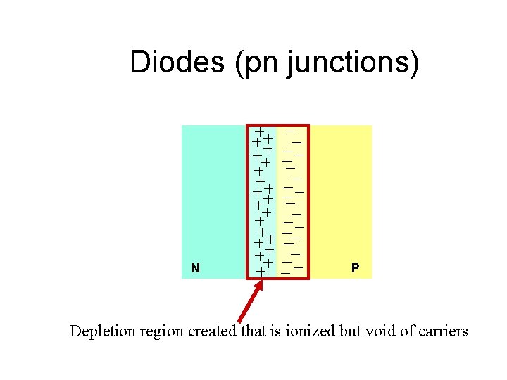
Diodes (pn junctions) N P Depletion region created that is ionized but void of carriers

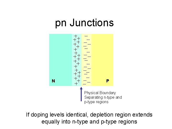
pn Junctions N P Physical Boundary Separating n-type and p-type regions If doping levels identical, depletion region extends equally into n-type and p-type regions

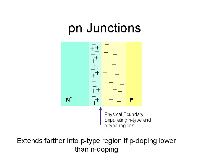
pn Junctions N+ P - Physical Boundary Separating n-type and p-type regions Extends farther into p-type region if p-doping lower than n-doping

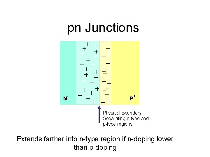
pn Junctions N - P + Physical Boundary Separating n-type and p-type regions Extends farther into n-type region if n-doping lower than p-doping

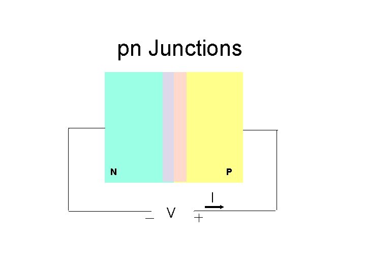
pn Junctions N P V I

pn Junctions I N P V I Diode Equation: JS= Sat Current Density A= Junction Cross Section Area VT=k. T/q n is approximately 1 V

Basic Devices and Device Models • • • Resistor Diode Capacitor MOSFET BJT

Capacitors • Types – Parallel Plate – Fringe – Junction

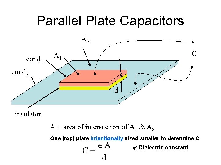
Parallel Plate Capacitors A 2 cond 1 C A 1 cond 2 d insulator A = area of intersection of A 1 & A 2 One (top) plate intentionally sized smaller to determine C : Dielectric constant

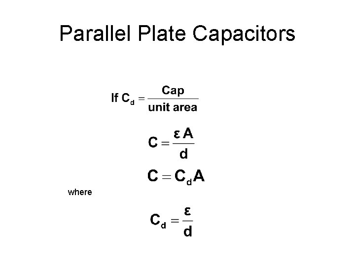
Parallel Plate Capacitors where

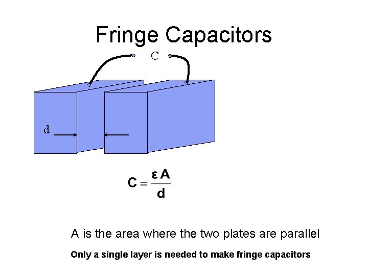
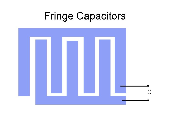
Fringe Capacitors C d A is the area where the two plates are parallel Only a single layer is needed to make fringe capacitors

Fringe Capacitors C

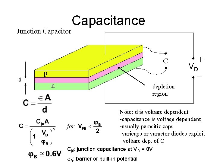
Junction Capacitor Capacitance C d p n d VD depletion region Note: d is voltage dependent -capacitance is voltage dependent -usually parasitic caps -varicaps or varactor diodes exploit voltage dep. of C Cj 0: junction capacitance at VD = 0 V B: barrier or built-in potential

Basic Devices and Device Models • • • Resistor Diode Capacitor MOSFET BJT

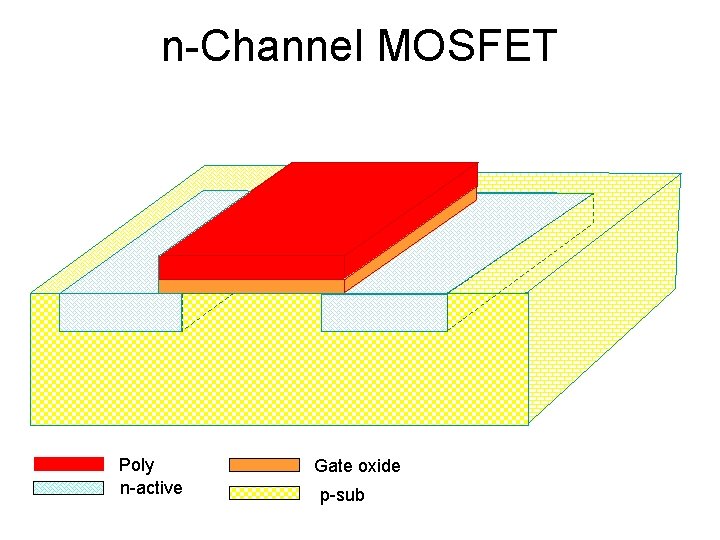
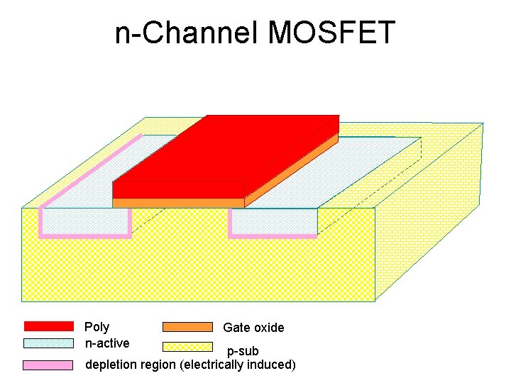
n-Channel MOSFET Poly n-active Gate oxide p-sub

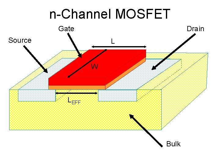
n-Channel MOSFET Gate Drain Source L W LEFF Bulk

n-Channel MOSFET Poly n-active Gate oxide p-sub depletion region (electrically induced)

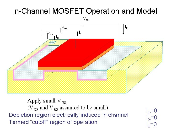
n-Channel MOSFET Operation and Model VDS ID VGS VBS IB IG Apply small VGS (VDS and VBS assumed to be small) Depletion region electrically induced in channel Termed “cutoff” region of operation ID=0 IG=0 IB=0

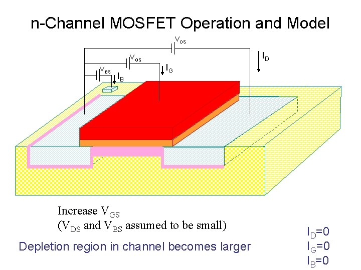
n-Channel MOSFET Operation and Model VDS ID VGS VBS IB IG Increase VGS (VDS and VBS assumed to be small) Depletion region in channel becomes larger ID=0 IG=0 IB=0

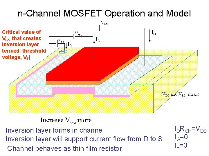
n-Channel MOSFET Operation and Model VDS Critical value of VGS that creates inversion layer termed threshold voltage, VT) ID VGS VBS IB IG (VDS and VBS small) Increase VGS more Inversion layer forms in channel Inversion layer will support current flow from D to S Channel behaves as thin-film resistor IDRCH=VDS IG=0 IB=0

n-Channel MOSFET Operation and Model VDS ID VGS VBS IB IG (VDS and VBS small) Increase VGS more Inversion layer in channel thickens RCH will decrease Termed “ohmic” or “triode” region of operation IDRCH=VDS IG=0 IB=0

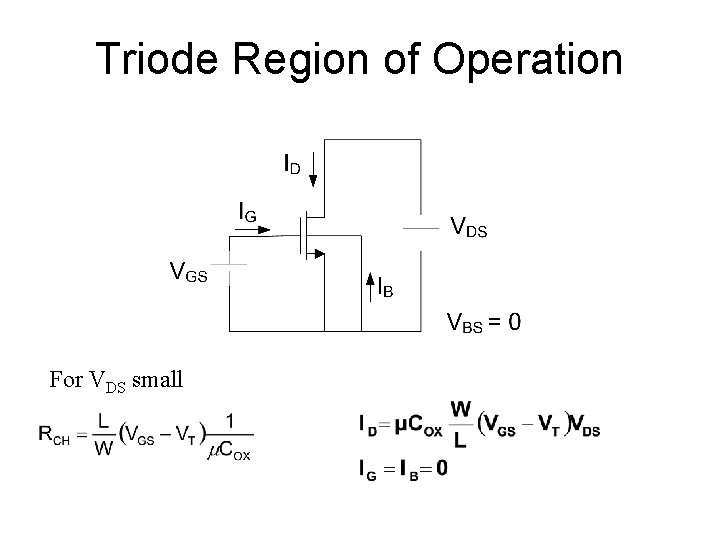
Triode Region of Operation For VDS small

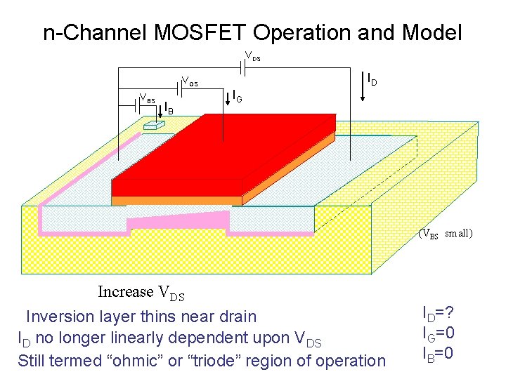
n-Channel MOSFET Operation and Model VDS ID VGS VBS IB IG (VBS small) Increase VDS Inversion layer thins near drain ID no longer linearly dependent upon VDS Still termed “ohmic” or “triode” region of operation ID=? IG=0 IB=0

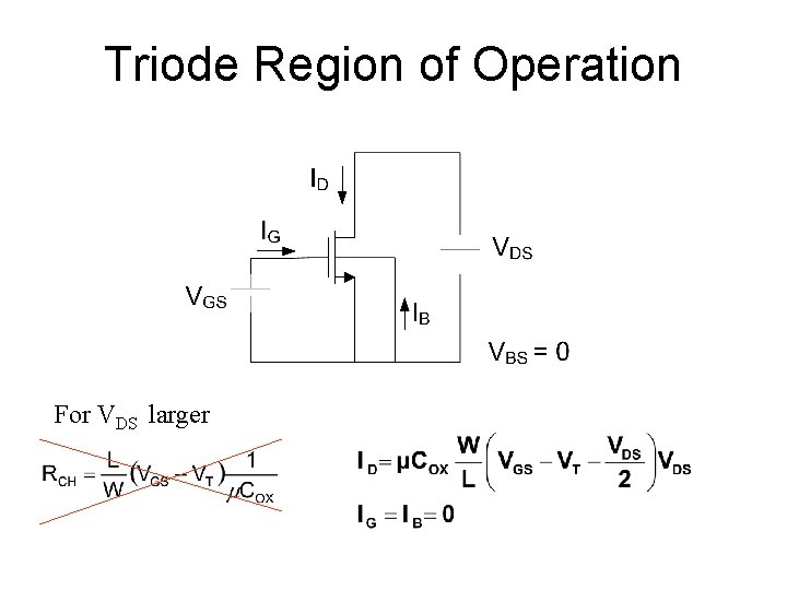
Triode Region of Operation For VDS larger

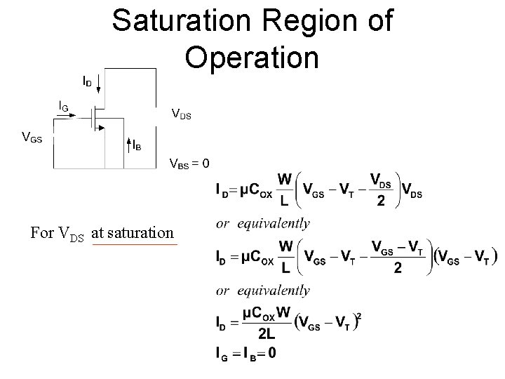
n-Channel MOSFET Operation and Model VDS ID VGS VBS IB IG (VBS small) Increase VDS even more Inversion layer disappears near drain Termed “saturation”region of operation Saturation first occurs when VDS=VGS-VT ID=? IG=0 IB=0

Saturation Region of Operation For VDS at saturation

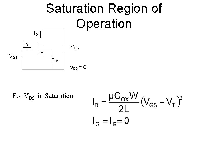
n-Channel MOSFET Operation and Model VDS ID VGS VBS IB IG (VBS small) Increase VDS even more (beyond VGS-VT) Nothing much changes !! Termed “saturation”region of operation ID=? IG=0 IB=0

Saturation Region of Operation For VDS in Saturation

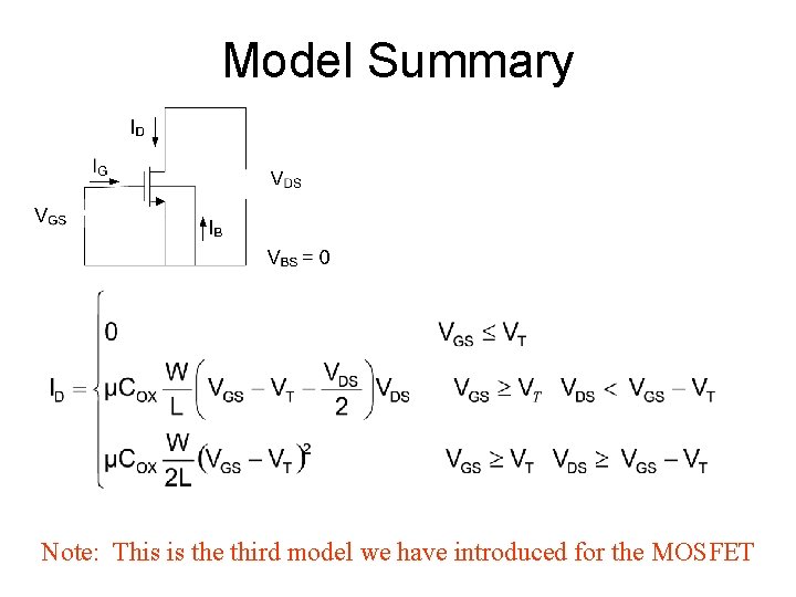
Model Summary Note: This is the third model we have introduced for the MOSFET