EE 40 Lecture 18 Josh Hug 8062010 EE


- Slides: 79

EE 40 Lecture 18 Josh Hug 8/06/2010 EE 40 Summer 2010 Hug 1

Logistics • HW 8 due today @5 PM – short but tough • Mini-midterm 3 next Wednesday – 80/160 points will be a take-home set of design problems which will utilize techniques we’ve covered in class • Posted online – Other 80/160 will be an in class midterm covering HW 7 and HW 8 • Final will include Friday and Monday lecture, Midterm won’t – Design problems will provide practice EE 40 Summer 2010 Hug 2

Project 2 • Project 2 demos next Wednesday (after midterm), need two things to be “done”: – Check-off: Verifying that your circuit works - can optionally be done before Wednesday if you’re worried about circuit breaking before presentation – Presentation: Asking you questions about why your circuit works – No lab report • Presentation will be Wednesday in lab – 1: 15 PM until we’re done (~3: 00 PM? ) – Cooper, Onur, and I will walk around asking questions – Bring your circuit even if function is checked-off EE 40 Summer 2010 Hug 3

Project 2 • Booster lab actually due next week – For Booster lab, ignore circuit simulation, though it may be instructive to try the Falstad simulator • Project 2 demos next Wednesday (after midterm) EE 40 Summer 2010 Hug 4

EE 40 this Summer • We’ve covered a terrifyingly large number of things for only 7 weeks • By this time last semester, they had just finished RC and RL circuits and hadn’t started phasors yet, we’ve done all that and: – – – – Phasors Transfer Functions and Filtering Real and Reactive Power Bode Plots Qualitatively: Integrated Circuits Manufacturing Defining Digital Systems MOSFET structure and 3 models of the MOSFET Discussed analysis and design of transistor circuits • Function • Delay • Power Dissipation – Diode circuit analysis • You’ll pardon me if we have a little fun… EE 40 Summer 2010 Hug 5

Rewatching Lectures • As you remember in lecture this week, I realized I like saying “kind of” and “sort of” a lot – I rewatched some of my lectures, and it is worse than I had feared – Annihilates any residual professorial gravitas remaining to a short grad student with long hair • As expected, youtube comments are less than friendly • Let’s set the record straight, i. Clicker style EE 40 Summer 2010 Hug 6

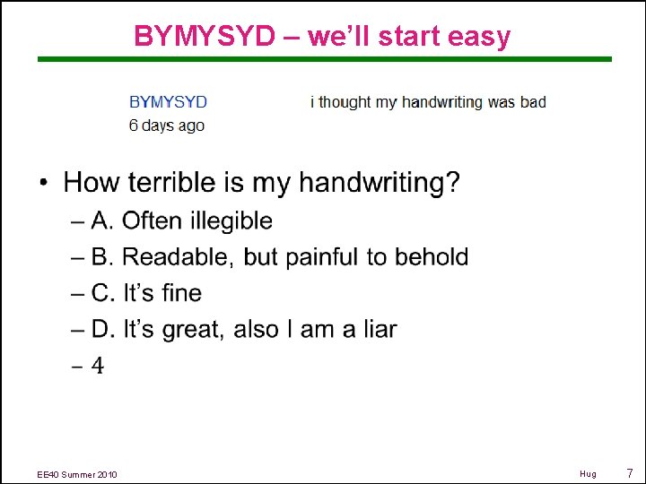
BYMYSYD – we’ll start easy • EE 40 Summer 2010 Hug 7

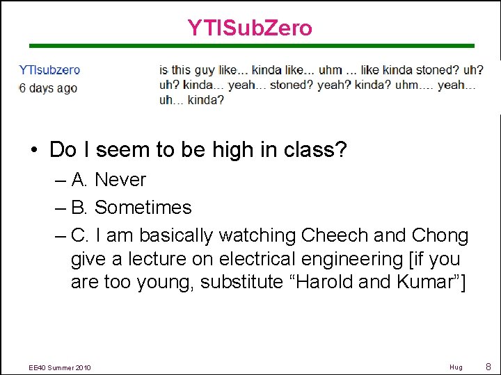
YTISub. Zero • Do I seem to be high in class? – A. Never – B. Sometimes – C. I am basically watching Cheech and Chong give a lecture on electrical engineering [if you are too young, substitute “Harold and Kumar”] EE 40 Summer 2010 Hug 8

Yokombo – Lecture on RC and RL circuits • How freakish am I? – A. Seem pretty normal – B. Normal, except the weird walk – C. Eccentric, in a safely professorish way – D. I have on occasion been afraid to come to class EE 40 Summer 2010 Hug 9

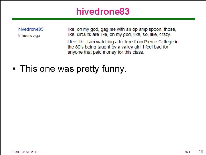
hivedrone 83 • This one was pretty funny. EE 40 Summer 2010 Hug 10

Today • Intro to semiconductor physics • Diodes and PN-Junctions EE 40 Summer 2010 Hug 11

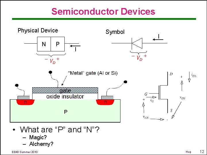
Semiconductor Devices Physical Device N - P Symbol I + I - + • What are “P” and “N”? – Magic? – Alchemy? EE 40 Summer 2010 Hug 12

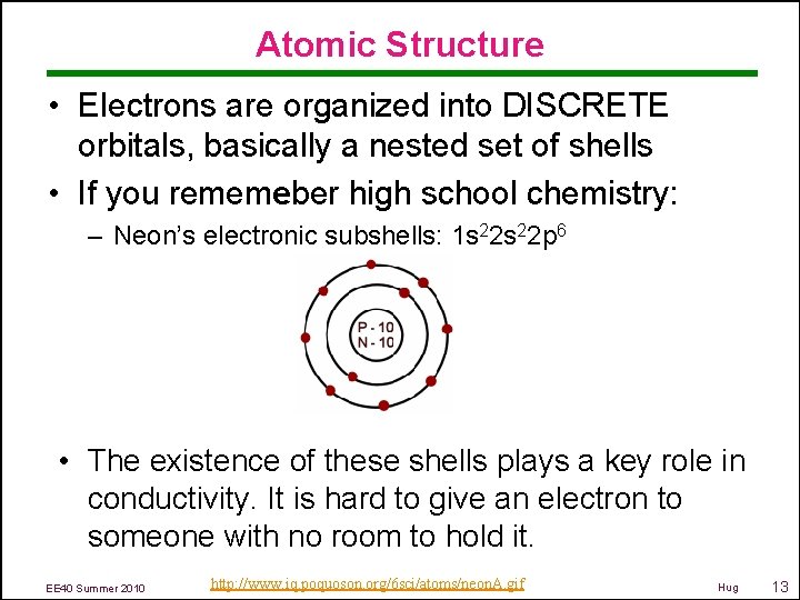
Atomic Structure • Electrons are organized into DISCRETE orbitals, basically a nested set of shells • If you rememeber high school chemistry: – Neon’s electronic subshells: 1 s 22 p 6 • The existence of these shells plays a key role in conductivity. It is hard to give an electron to someone with no room to hold it. EE 40 Summer 2010 http: //www. iq. poquoson. org/6 sci/atoms/neon. A. gif Hug 13

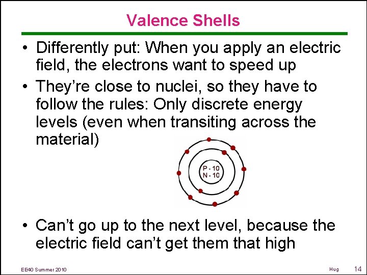
Valence Shells • Differently put: When you apply an electric field, the electrons want to speed up • They’re close to nuclei, so they have to follow the rules: Only discrete energy levels (even when transiting across the material) • Can’t go up to the next level, because the electric field can’t get them that high EE 40 Summer 2010 Hug 14

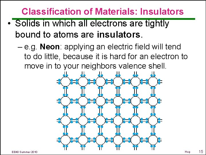
Classification of Materials: Insulators • Solids in which all electrons are tightly bound to atoms are insulators. – e. g. Neon: applying an electric field will tend to do little, because it is hard for an electron to move in to your neighbors valence shell. EE 40 Summer 2010 Hug 15

Electrons in Conductors and Insulators • Solids with “free electrons” – that is electrons not directly involved in the inter-atomic bonding- are the familiar metals (Cu, Al, Fe, Au, etc) – Often 1 free electron per atom • Solids with no free electrons are the familiar insulators (glass, quartz crystals, ceramics, etc. ) EE 40 Summer 2010 Hug 16

Resistance of a Metal vs. Temperature • How does the resistance of a metal vary with temperature? – A. Resistance increases as temperature goes up – B. Resistance decreases as temperature goes up EE 40 Summer 2010 Hug 17

Why? • In a hot metal everything is moving around a lot more • Electrons trying to get from point a to point b are constantly running into this big disorderly surface fluctuating around them • A very cold metal, by contrast, sits relatively still, so electrons can zoom along the lattice unhindered EE 40 Summer 2010 Hug 18

Electrons in Semiconductors • Silicon is an insulator, but at higher temperatures some of the bonding electrons can get free and make it a little conducting – hence the term “semiconductor” • Pure silicon is a poor conductor (and a poor insulator). It has 4 valence electrons, all of which are needed to bond with nearest neighbors. No free electrons. EE 40 Summer 2010 Hug 19

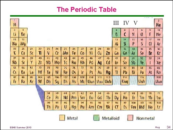
The Periodic Table III IV V EE 40 Summer 2010 Hug 20

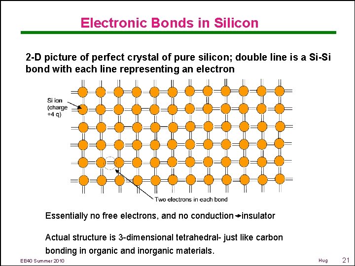
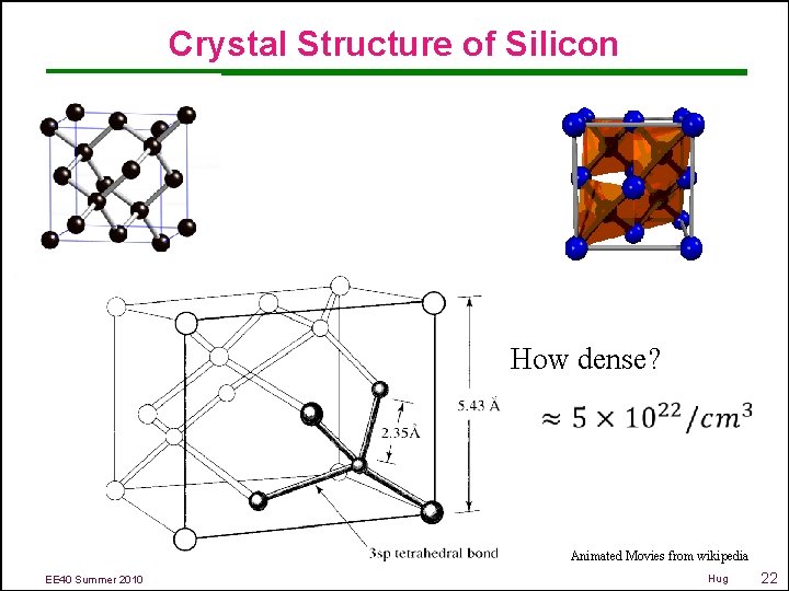
Electronic Bonds in Silicon 2 -D picture of perfect crystal of pure silicon; double line is a Si-Si bond with each line representing an electron Essentially no free electrons, and no conduction - insulator Actual structure is 3 -dimensional tetrahedral- just like carbon bonding in organic and inorganic materials. EE 40 Summer 2010 Hug 21

Crystal Structure of Silicon How dense? Animated Movies from wikipedia EE 40 Summer 2010 Hug 22

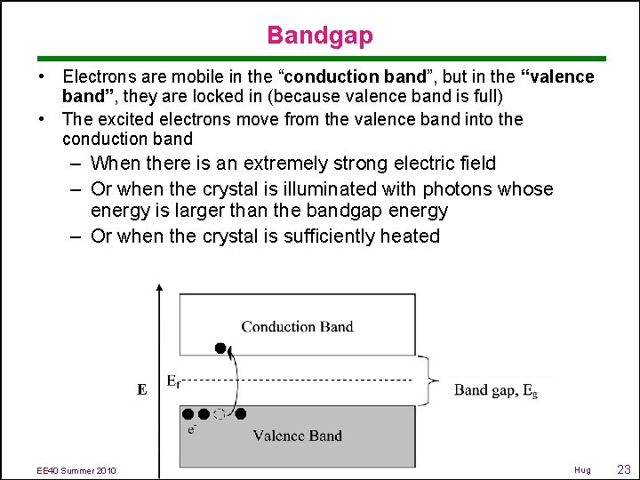
Bandgap • Electrons are mobile in the “conduction band”, but in the “valence band”, they are locked in (because valence band is full) • The excited electrons move from the valence band into the conduction band – When there is an extremely strong electric field – Or when the crystal is illuminated with photons whose energy is larger than the bandgap energy – Or when the crystal is sufficiently heated EE 40 Summer 2010 Hug 23

Semiconductors • Resistance DECREASES with temperature – Yes, everything is jostling around more! • More electrons can be shaken free to move around • While traveling, these electrons endure scattering as they repeatedly run into the jostling landscape. Heat exacerbates this – You can’t win if you don’t play • More players • Worse odds • Still get more absolute number of successes EE 40 Summer 2010 Hug 24

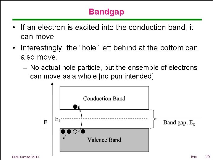
Bandgap • If an electron is excited into the conduction band, it can move • Interestingly, the “hole” left behind at the bottom can also move. – No actual hole particle, but the ensemble of electrons can move as a whole [no pun intended] EE 40 Summer 2010 Hug 25

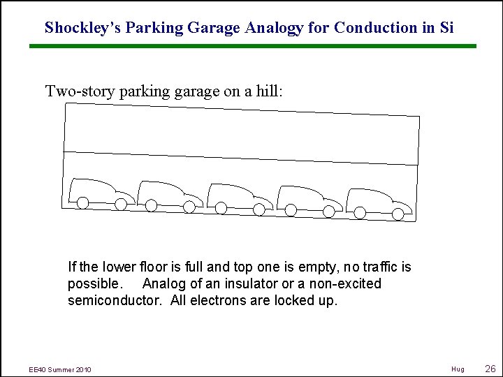
Shockley’s Parking Garage Analogy for Conduction in Si Two-story parking garage on a hill: If the lower floor is full and top one is empty, no traffic is possible. Analog of an insulator or a non-excited semiconductor. All electrons are locked up. EE 40 Summer 2010 Hug 26

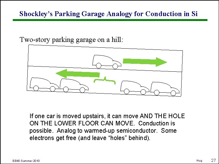
Shockley’s Parking Garage Analogy for Conduction in Si Two-story parking garage on a hill: If one car is moved upstairs, it can move AND THE HOLE ON THE LOWER FLOOR CAN MOVE. Conduction is possible. Analog to warmed-up semiconductor. Some electrons get free (and leave “holes” behind). EE 40 Summer 2010 Hug 27

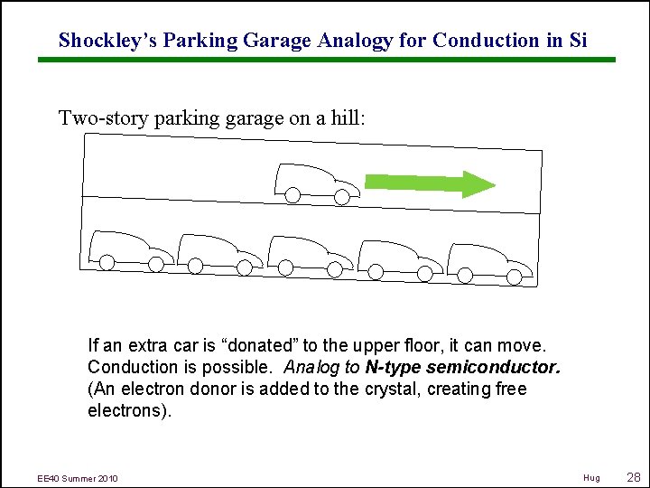
Shockley’s Parking Garage Analogy for Conduction in Si Two-story parking garage on a hill: If an extra car is “donated” to the upper floor, it can move. Conduction is possible. Analog to N-type semiconductor. (An electron donor is added to the crystal, creating free electrons). EE 40 Summer 2010 Hug 28

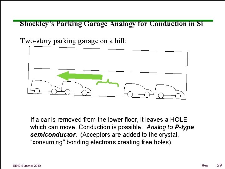
Shockley’s Parking Garage Analogy for Conduction in Si Two-story parking garage on a hill: If a car is removed from the lower floor, it leaves a HOLE which can move. Conduction is possible. Analog to P-type semiconductor. (Acceptors are added to the crystal, “consuming” bonding electrons, creating free holes). EE 40 Summer 2010 Hug 29

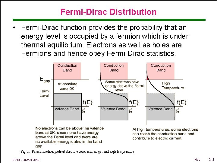
Fermi-Dirac Distribution • Fermi-Dirac function provides the probability that an energy level is occupied by a fermion which is under thermal equilibrium. Electrons as well as holes are Fermions and hence obey Fermi-Dirac statistics. Fig. 5. Fermi function plots at absolute zero, mid-range, and high temperature. EE 40 Summer 2010 Hug 30

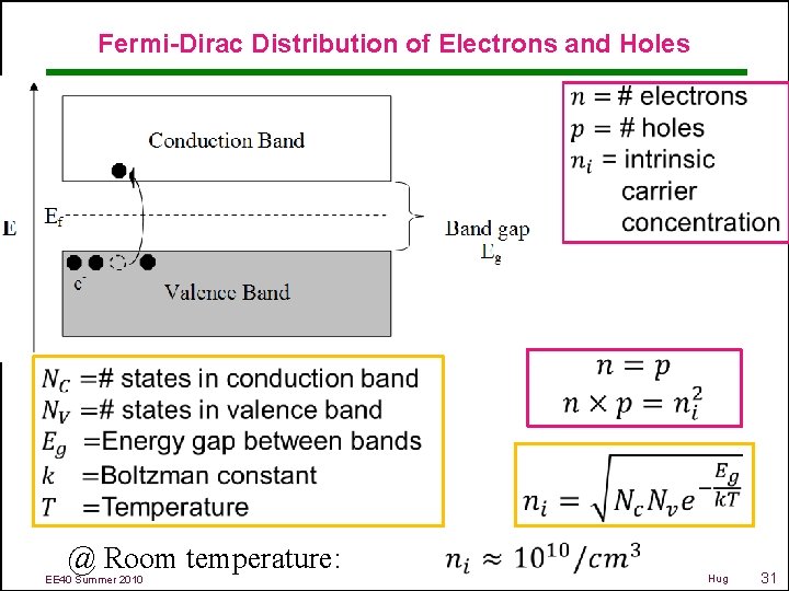
Fermi-Dirac Distribution of Electrons and Holes @ Room temperature: EE 40 Summer 2010 Hug 31

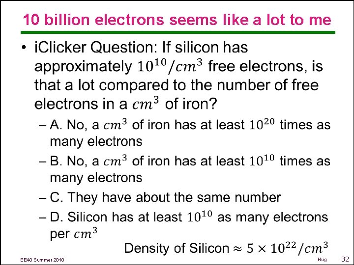
10 billion electrons seems like a lot to me • EE 40 Summer 2010 Hug 32

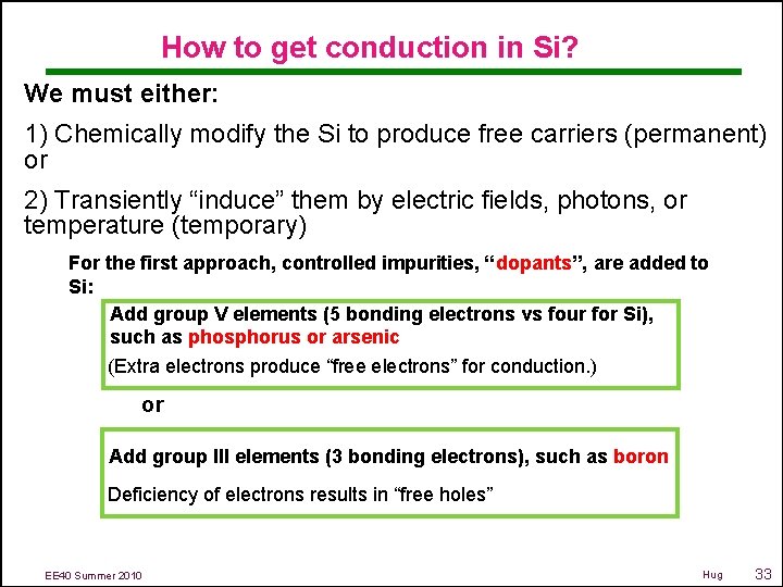
How to get conduction in Si? We must either: 1) Chemically modify the Si to produce free carriers (permanent) or 2) Transiently “induce” them by electric fields, photons, or temperature (temporary) For the first approach, controlled impurities, “dopants”, are added to Si: Add group V elements (5 bonding electrons vs four for Si), such as phosphorus or arsenic (Extra electrons produce “free electrons” for conduction. ) or Add group III elements (3 bonding electrons), such as boron Deficiency of electrons results in “free holes” EE 40 Summer 2010 Hug 33

The Periodic Table III IV V EE 40 Summer 2010 Hug 34

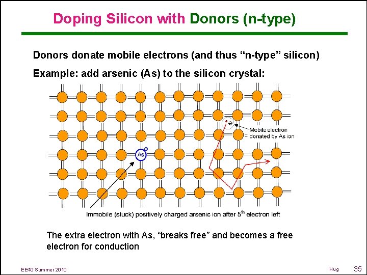
Doping Silicon with Donors (n-type) Donors donate mobile electrons (and thus “n-type” silicon) Example: add arsenic (As) to the silicon crystal: The extra electron with As, “breaks free” and becomes a free electron for conduction EE 40 Summer 2010 Hug 35

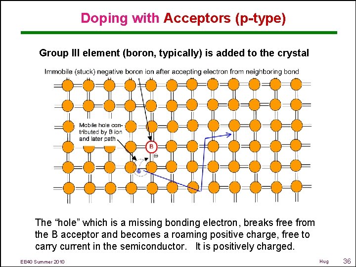
Doping with Acceptors (p-type) Group III element (boron, typically) is added to the crystal The “hole” which is a missing bonding electron, breaks free from the B acceptor and becomes a roaming positive charge, free to carry current in the semiconductor. It is positively charged. EE 40 Summer 2010 Hug 36

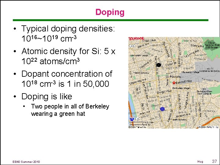
Doping • Typical doping densities: 1016~1019 cm-3 • Atomic density for Si: 5 x 10²² atoms/cm 3 • Dopant concentration of 1018 cm-3 is 1 in 50, 000 • Doping is like • Two people in all of Berkeley wearing a green hat EE 40 Summer 2010 Hug 37

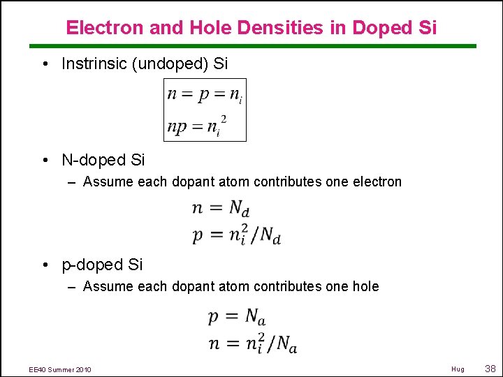
Electron and Hole Densities in Doped Si • Instrinsic (undoped) Si • N-doped Si – Assume each dopant atom contributes one electron • p-doped Si – Assume each dopant atom contributes one hole EE 40 Summer 2010 Hug 38

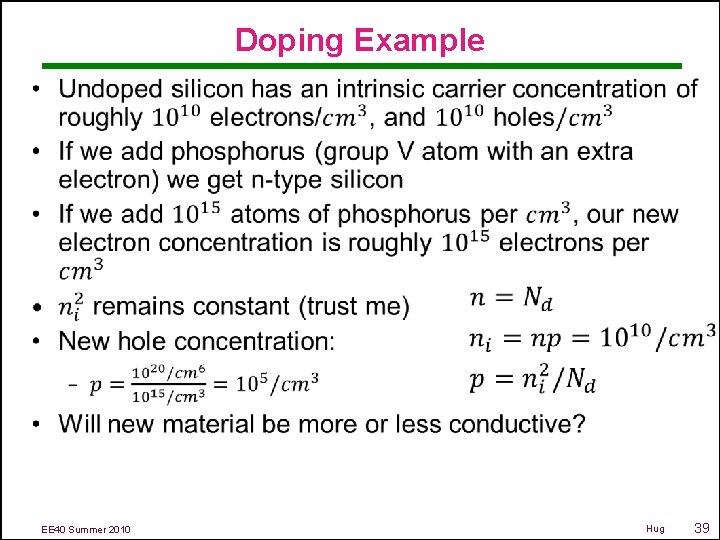
Doping Example • EE 40 Summer 2010 Hug 39

Summary of n- and p-type silicon Pure silicon is an insulator. At high temperatures it conducts weakly. If we add an impurity with extra electrons (e. g. arsenic, phosphorus) these extra electrons are set free and we have a pretty good conductor (n-type silicon). If we add an impurity with a deficit of electrons (e. g. boron) then bonding electrons are missing (holes), and the resulting holes can move around … again a pretty good conductor (p-type silicon) Now what is really interesting is when we join n-type and p-type silicon, that is make a pn junction. It has interesting electrical properties. EE 40 Summer 2010 Hug 40

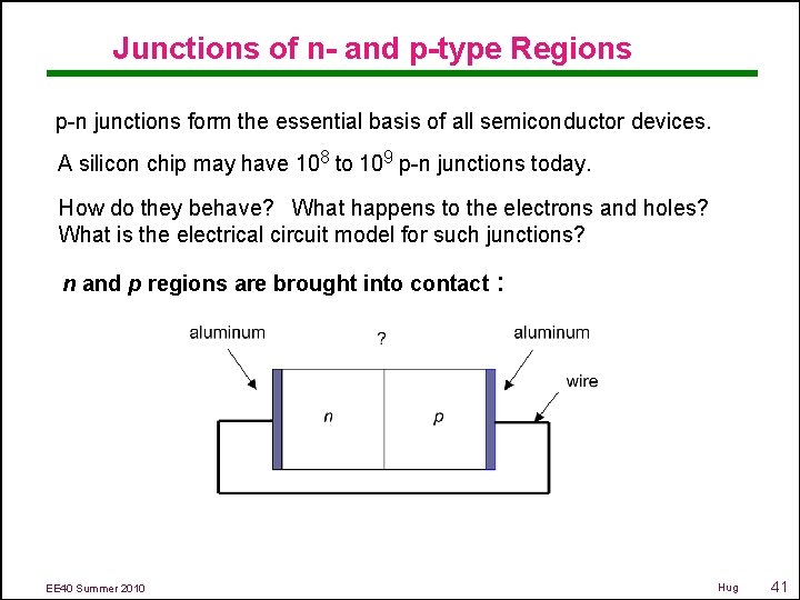
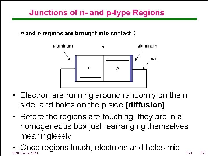
Junctions of n- and p-type Regions p-n junctions form the essential basis of all semiconductor devices. A silicon chip may have 108 to 109 p-n junctions today. How do they behave? What happens to the electrons and holes? What is the electrical circuit model for such junctions? n and p regions are brought into contact EE 40 Summer 2010 : Hug 41

Junctions of n- and p-type Regions n and p regions are brought into contact : • Electron are running around randomly on the n side, and holes on the p side [diffusion] • Before the regions are touching, they are in a homogeneous box just rearranging themselves meaninglessly • Once regions touch, electrons and holes mix EE 40 Summer 2010 Hug 42

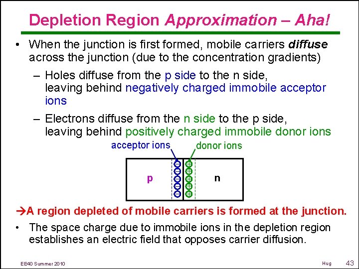
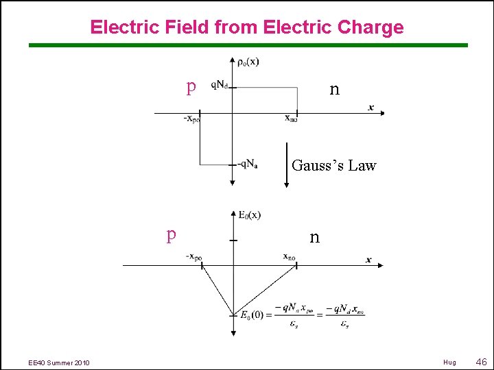
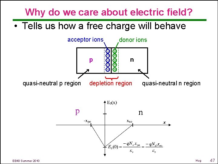
Depletion Region Approximation – Aha! • When the junction is first formed, mobile carriers diffuse across the junction (due to the concentration gradients) – Holes diffuse from the p side to the n side, leaving behind negatively charged immobile acceptor ions – Electrons diffuse from the n side to the p side, leaving behind positively charged immobile donor ions acceptor ions donor ions – + – + p n – + A region depleted of mobile carriers is formed at the junction. • The space charge due to immobile ions in the depletion region establishes an electric field that opposes carrier diffusion. EE 40 Summer 2010 Hug 43

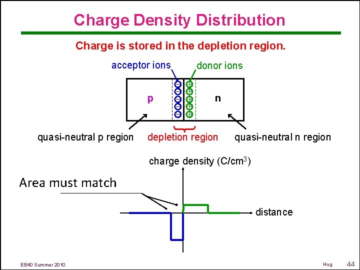
Charge Density Distribution Charge is stored in the depletion region. acceptor ions donor ions – + – + p n – + quasi-neutral p region depletion region quasi-neutral n region charge density (C/cm 3) Area must match distance EE 40 Summer 2010 Hug 44

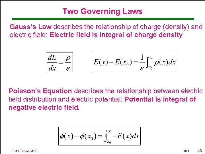
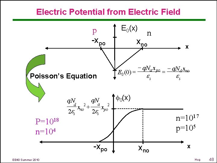
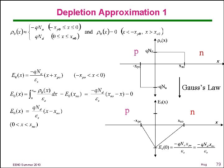
Two Governing Laws Gauss’s Law describes the relationship of charge (density) and electric field: Electric field is integral of charge density Poisson’s Equation describes the relationship between electric field distribution and electric potential: Potential is integral of negative electric field. EE 40 Summer 2010 Hug 45

Electric Field from Electric Charge p n Gauss’s Law p EE 40 Summer 2010 n Hug 46

Why do we care about electric field? • Tells us how a free charge will behave acceptor ions donor ions – + – + p n – + quasi-neutral p region p EE 40 Summer 2010 depletion region quasi-neutral n region n Hug 47

Electric Potential from Electric Field p -xpo d 2 es xno 2 + q. N a 2 es xpo 2 n xno E 0 (0) = Poisson’s Equation q. N E 0(x) - q. Na x po es es n=1017 p=105 n=104 EE 40 Summer 2010 = q. Nd xno f 0(x) P=1018 -xpo x xno x Hug 48

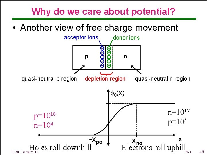
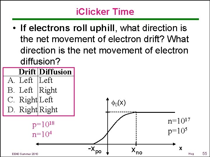
Why do we care about potential? • Another view of free charge movement acceptor ions donor ions – + – + p n – + quasi-neutral p region depletion region quasi-neutral n region f 0(x) p=1018 n=104 n=1017 p=105 x -xpo xno Holes roll downhill Electrons roll uphill EE 40 Summer 2010 Hug 49

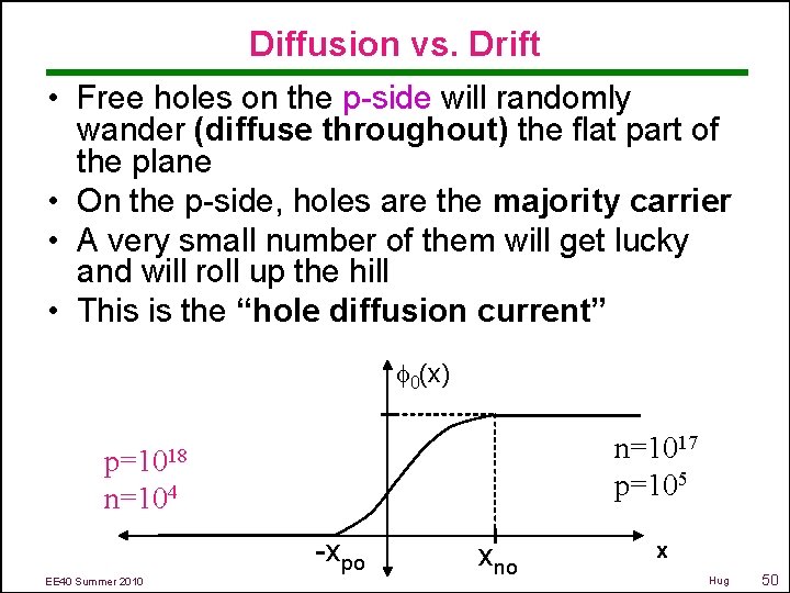
Diffusion vs. Drift • Free holes on the p-side will randomly wander (diffuse throughout) the flat part of the plane • On the p-side, holes are the majority carrier • A very small number of them will get lucky and will roll up the hill • This is the “hole diffusion current” f 0(x) n=1017 p=105 p=1018 n=104 -xpo EE 40 Summer 2010 xno x Hug 50

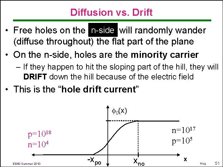
Diffusion vs. Drift n-side • Free holes on the will randomly wander (diffuse throughout) the flat part of the plane • On the n-side, holes are the minority carrier – If they happen to hit the sloping part of the hill, they will DRIFT down the hill because of the electric field • This is the “hole drift current” f 0(x) n=1017 p=105 p=1018 n=104 EE 40 Summer 2010 -xpo xno x Hug 51

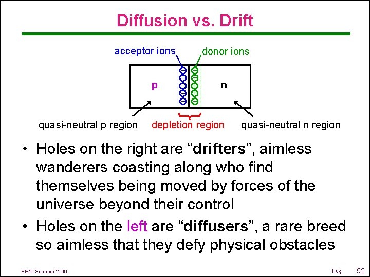
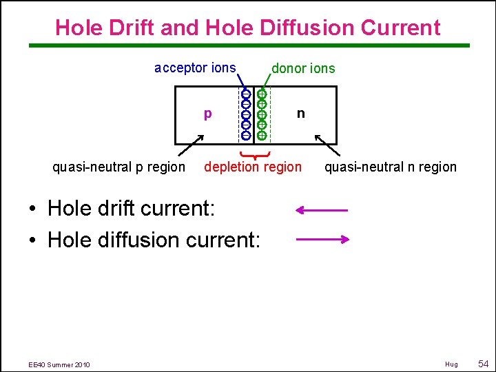
Diffusion vs. Drift acceptor ions donor ions – + – + p n – + quasi-neutral p region depletion region quasi-neutral n region • Holes on the right are “drifters”, aimless wanderers coasting along who find themselves being moved by forces of the universe beyond their control • Holes on the left are “diffusers”, a rare breed so aimless that they defy physical obstacles EE 40 Summer 2010 Hug 52

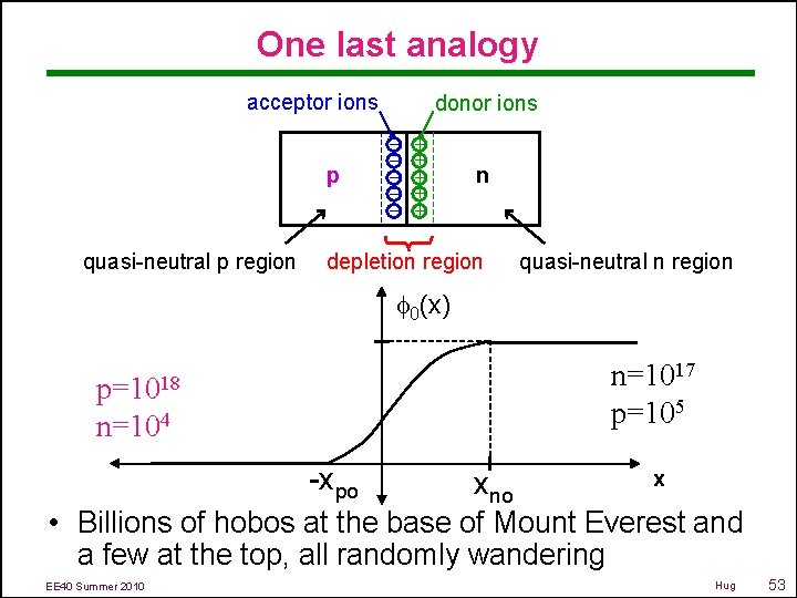
One last analogy acceptor ions donor ions – + – + p n – + quasi-neutral p region depletion region quasi-neutral n region f 0(x) n=1017 p=105 p=1018 n=104 -xpo xno x • Billions of hobos at the base of Mount Everest and a few at the top, all randomly wandering EE 40 Summer 2010 Hug 53

Hole Drift and Hole Diffusion Current acceptor ions donor ions – + – + p n – + quasi-neutral p region depletion region quasi-neutral n region • Hole drift current: • Hole diffusion current: EE 40 Summer 2010 Hug 54

i. Clicker Time • If electrons roll uphill, what direction is the net movement of electron drift? What direction is the net movement of electron diffusion? A. B. C. D. Drift Diffusion Left Right Left Right f 0(x) n=1017 p=105 p=1018 n=104 EE 40 Summer 2010 -xpo xno x Hug 55

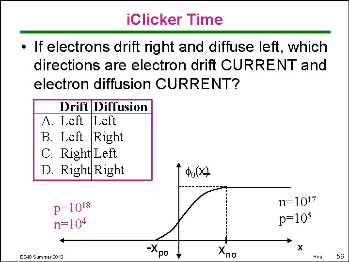
i. Clicker Time • If electrons drift right and diffuse left, which directions are electron drift CURRENT and electron diffusion CURRENT? A. B. C. D. Drift Diffusion Left Right Left Right f 0(x) n=1017 p=105 p=1018 n=104 EE 40 Summer 2010 -xpo xno x Hug 56

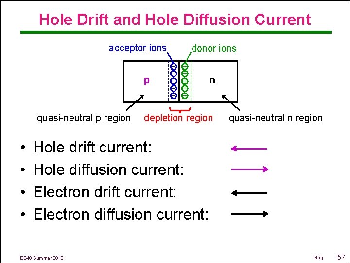
Hole Drift and Hole Diffusion Current acceptor ions donor ions – + – + p n – + quasi-neutral p region • • depletion region quasi-neutral n region Hole drift current: Hole diffusion current: Electron drift current: Electron diffusion current: EE 40 Summer 2010 Hug 57

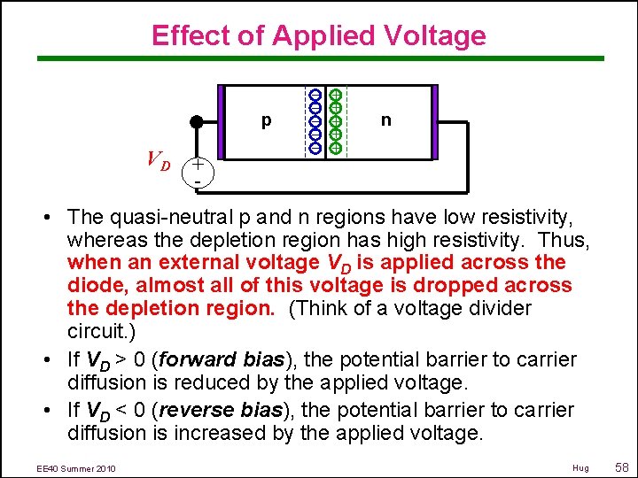
Effect of Applied Voltage VD + - – + – + p n – + • The quasi-neutral p and n regions have low resistivity, whereas the depletion region has high resistivity. Thus, when an external voltage VD is applied across the diode, almost all of this voltage is dropped across the depletion region. (Think of a voltage divider circuit. ) • If VD > 0 (forward bias), the potential barrier to carrier diffusion is reduced by the applied voltage. • If VD < 0 (reverse bias), the potential barrier to carrier diffusion is increased by the applied voltage. EE 40 Summer 2010 Hug 58

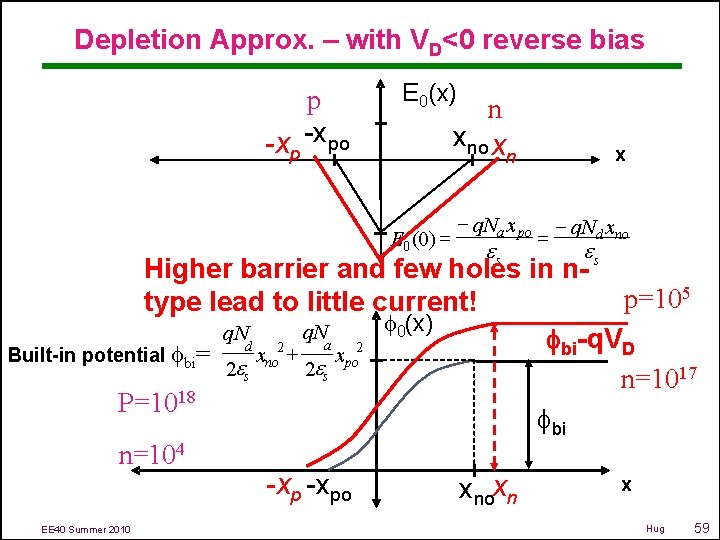
Depletion Approx. – with VD<0 reverse bias p -xpo E 0(x) n xno x n E 0 (0) = - q. Na x po es x = q. Nd xno es Higher barrier and few holes in np=105 type lead to little current! f 0(x) q. N fbi-q. VD a d Built-in potential fbi= xno 2 + xpo 2 2 es n=1017 P=1018 fbi n=104 x -xpo xnoxn EE 40 Summer 2010 Hug 59

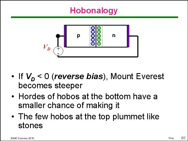
Hobonalogy VD + - – + – + p n – + • If VD < 0 (reverse bias), Mount Everest becomes steeper • Hordes of hobos at the bottom have a smaller chance of making it • The few hobos at the top plummet like stones EE 40 Summer 2010 Hug 60

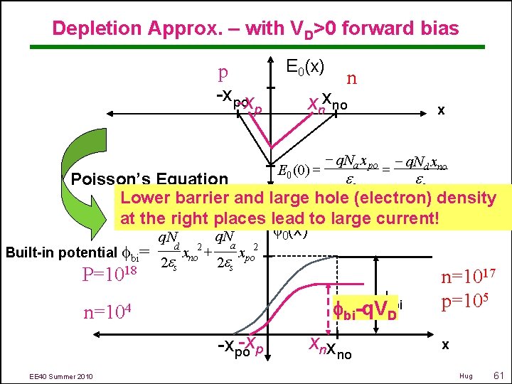
Depletion Approx. – with VD>0 forward bias p -xpo -x E 0(x) p n xnxno E 0 (0) = - q. Na x po x = q. Nd xno es es Poisson’s Equation Lower barrier and large hole (electron) density at the right places lead to large current! f 0(x) q. N a d Built-in potential fbi= xno 2 + xpo 2 P=1018 2 es fbi-q. VD n=104 -xpo EE 40 Summer 2010 xnx no n=1017 p=105 x Hug 61

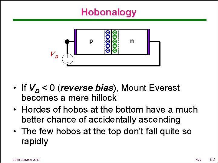
Hobonalogy VD + - – + – + p n – + • If VD < 0 (reverse bias), Mount Everest becomes a mere hillock • Hordes of hobos at the bottom have a much better chance of accidentally ascending • The few hobos at the top don’t fall quite so rapidly EE 40 Summer 2010 Hug 62

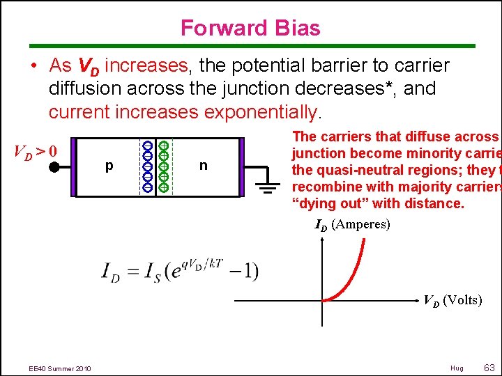
Forward Bias • As VD increases, the potential barrier to carrier diffusion across the junction decreases*, and current increases exponentially. VD > 0 – + – + p n – + The carriers that diffuse across junction become minority carrie the quasi-neutral regions; they t recombine with majority carriers “dying out” with distance. ID (Amperes) VD (Volts) EE 40 Summer 2010 Hug 63

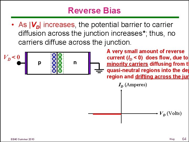
Reverse Bias • As |VD| increases, the potential barrier to carrier diffusion across the junction increases*; thus, no carriers diffuse across the junction. VD < 0 – + – + p n – + A very small amount of reverse current (ID < 0) does flow, due to minority carriers diffusing from th quasi-neutral regions into the dep region and drifting across the jun ID (Amperes) VD (Volts) EE 40 Summer 2010 Hug 64

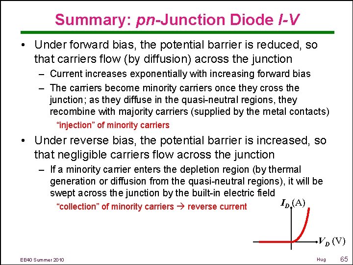
Summary: pn-Junction Diode I-V • Under forward bias, the potential barrier is reduced, so that carriers flow (by diffusion) across the junction – Current increases exponentially with increasing forward bias – The carriers become minority carriers once they cross the junction; as they diffuse in the quasi-neutral regions, they recombine with majority carriers (supplied by the metal contacts) “injection” of minority carriers • Under reverse bias, the potential barrier is increased, so that negligible carriers flow across the junction – If a minority carrier enters the depletion region (by thermal generation or diffusion from the quasi-neutral regions), it will be swept across the junction by the built-in electric field ID (A) “collection” of minority carriers reverse current VD (V) EE 40 Summer 2010 Hug 65

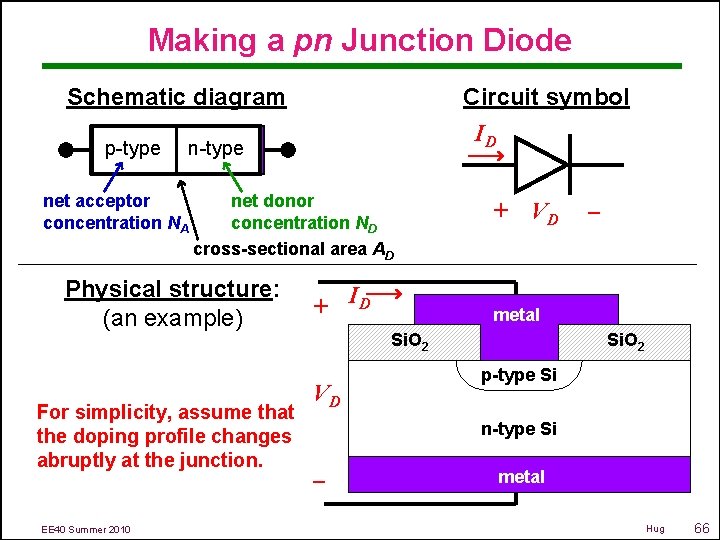
Making a pn Junction Diode Schematic diagram Circuit symbol ID p-type net acceptor concentration NA net donor concentration ND cross-sectional area AD Physical structure: (an example) For simplicity, assume that the doping profile changes abruptly at the junction. EE 40 Summer 2010 + ID + VD metal Si. O 2 VD – Si. O 2 p-type Si n-type Si – metal Hug 66

More than one way to get current flowing • Or there’s more than one way to move hobos around mountains • Electric field is the obvious way • Can also create electron/hole pairs, for example, with light EE 40 Summer 2010 Hug 67

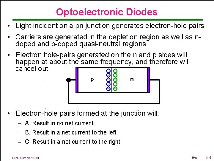
Optoelectronic Diodes • Light incident on a pn junction generates electron-hole pairs • Carriers are generated in the depletion region as well as ndoped and p-doped quasi-neutral regions. • Electron hole-pairs generated on the n and p sides will happen at about the same frequency, and therefore will cancel out – + – + p n – + • Electron-hole pairs formed at the junction will: – A. Result in no net current – B. Result in a net current to the left – C. Result in a net current to the right EE 40 Summer 2010 Hug 68

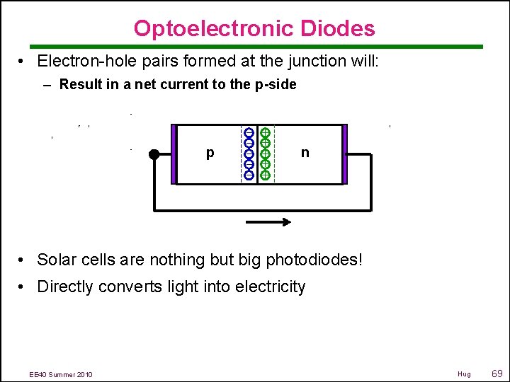
Optoelectronic Diodes • Electron-hole pairs formed at the junction will: – Result in a net current to the p-side – + – + p n – + • Solar cells are nothing but big photodiodes! • Directly converts light into electricity EE 40 Summer 2010 Hug 69

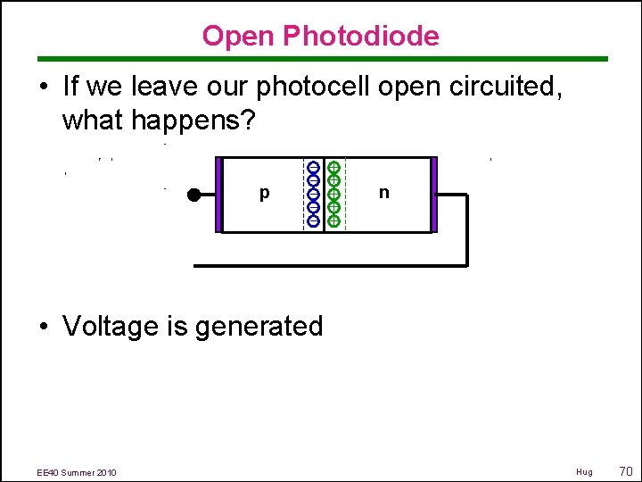
Open Photodiode • If we leave our photocell open circuited, what happens? – + – + p n – + • Voltage is generated EE 40 Summer 2010 Hug 70

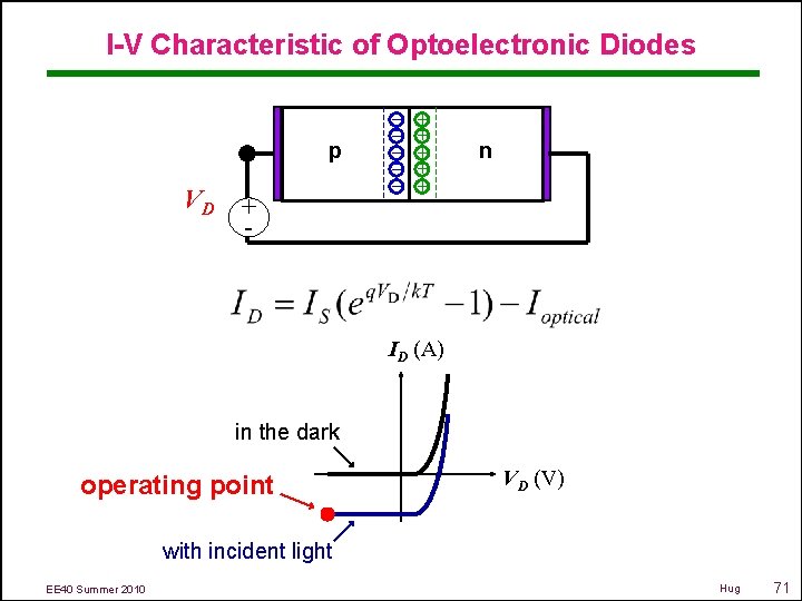
I-V Characteristic of Optoelectronic Diodes VD + - – + – + p n – + ID (A) in the dark operating point VD (V) with incident light EE 40 Summer 2010 Hug 71

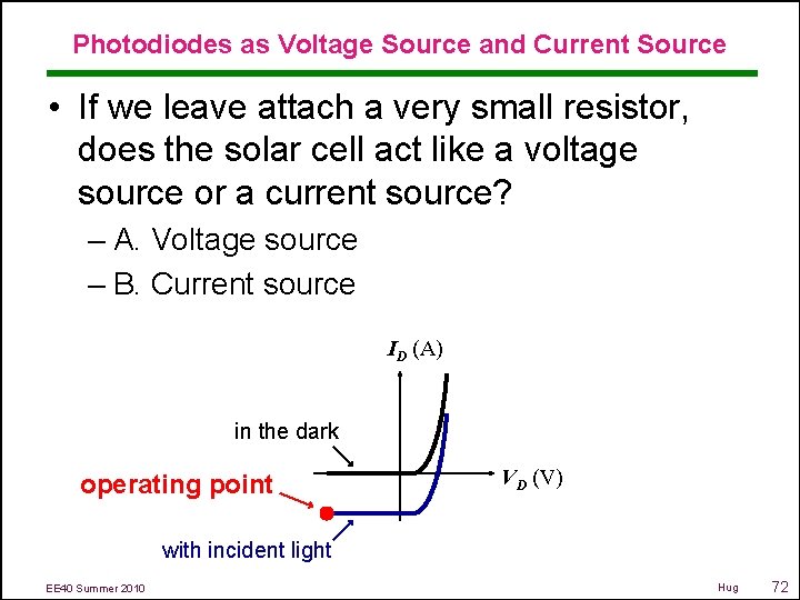
Photodiodes as Voltage Source and Current Source • If we leave attach a very small resistor, does the solar cell act like a voltage source or a current source? – A. Voltage source – B. Current source ID (A) in the dark operating point VD (V) with incident light EE 40 Summer 2010 Hug 72

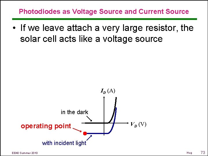
Photodiodes as Voltage Source and Current Source • If we leave attach a very large resistor, the solar cell acts like a voltage source ID (A) in the dark operating point VD (V) with incident light EE 40 Summer 2010 Hug 73

That’s all for today • Next time – Brief tiny look at MOSFET semiconductor physics (for ~5 minutes) – Course overview – Open Q&A: Send me questions beforehand for better answers – If somehow we aren’t done at this point, I’ll do a quick diode problem EE 40 Summer 2010 Hug 74

Extra Slides EE 40 Summer 2010 Hug 75

Design Problems • ALL WORK MUST BE DONE COMPLETELY SOLO! • Maximum allowed time will be 5 hours – Will be written so that it can be completed in approximately 2 hours • Allowed resources: – May use any textbook (incl. Google Books) – Anything posted on the EE 40 website – Only allowed websites are Google Books, wikipedia, and EE 40 websites – Not allowed to use other websites like facebook answers, yahoo answers, etc. even if you are reading other people’s responses – When in doubt, email me or text me – We will be very serious about cheating on this! EE 40 Summer 2010 Hug 76

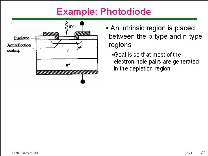
Example: Photodiode • An intrinsic region is placed between the p-type and n-type regions §Goal is so that most of the electron-hole pairs are generated in the depletion region EE 40 Summer 2010 Hug 77

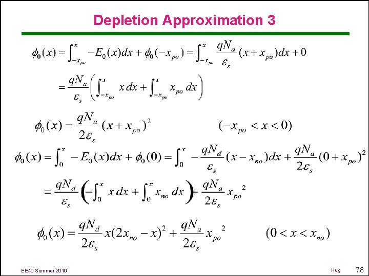
Depletion Approximation 3 EE 40 Summer 2010 Hug 78

Depletion Approximation 1 p n Gauss’s Law p EE 40 Summer 2010 n Hug 79