EE 40 Lecture 15 Josh Hug 7302010 EE



- Slides: 71

EE 40 Lecture 15 Josh Hug 7/30/2010 EE 40 Summer 2010 Hug 1

Logistics • HW 7 due Tuesday • HW 8 will be due next Friday • Homeworks will be less mathematically intense starting with the second half of HW 7 • Details on Project 2 demo and Mini. Midterm 3 details on Monday EE 40 Summer 2010 Hug 2

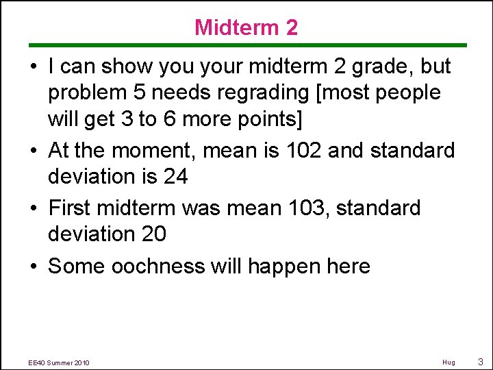
Midterm 2 • I can show your midterm 2 grade, but problem 5 needs regrading [most people will get 3 to 6 more points] • At the moment, mean is 102 and standard deviation is 24 • First midterm was mean 103, standard deviation 20 • Some oochness will happen here EE 40 Summer 2010 Hug 3

Logic Gates and Static Discipline • (On the board before we started) EE 40 Summer 2010 Hug 4

i. Clicker Warmup • We’re going to have a ton of i. Clicker questions today • A quick warmup. Have you played Starcraft 2? A. Yes B. No C. Starwhat? EE 40 Summer 2010 Hug 5

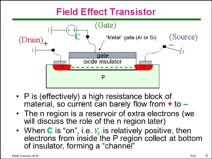
Field Effect Transistor + - (Drain) + (Gate) C (Source) – - - - - EE 40 Summer 2010 Hug 6

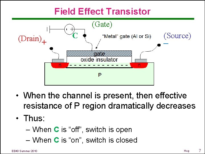
Field Effect Transistor + - (Drain) + (Gate) C (Source) – - - - - • When the channel is present, then effective resistance of P region dramatically decreases • Thus: – When C is “off”, switch is open – When C is “on”, switch is closed EE 40 Summer 2010 Hug 7

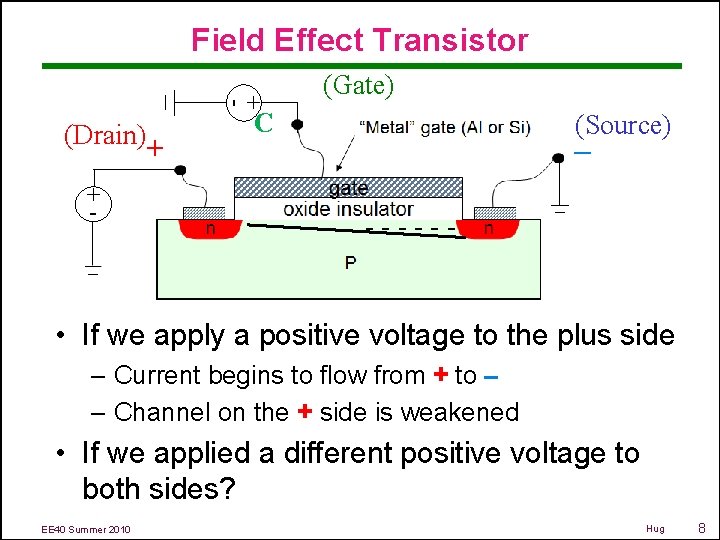
Field Effect Transistor + - (Drain) + - + (Gate) C (Source) – - - - • If we apply a positive voltage to the plus side – Current begins to flow from + to – – Channel on the + side is weakened • If we applied a different positive voltage to both sides? EE 40 Summer 2010 Hug 8

Field Effect Transistor Summary • “Switchiness” is due to a controlling voltage which induces a channel of free electrons • Extremely easy to make in unbelievable numbers • Ubiquitous in all computational technology everywhere EE 40 Summer 2010 Hug 9

Discussion Today • In discussion today, we’ll go over the physics of MOSFETs for those of you who are curious • Time permitting, we’ll discuss at a future date in class as well (so yeah, it will be slightly redundant) EE 40 Summer 2010 Hug 10

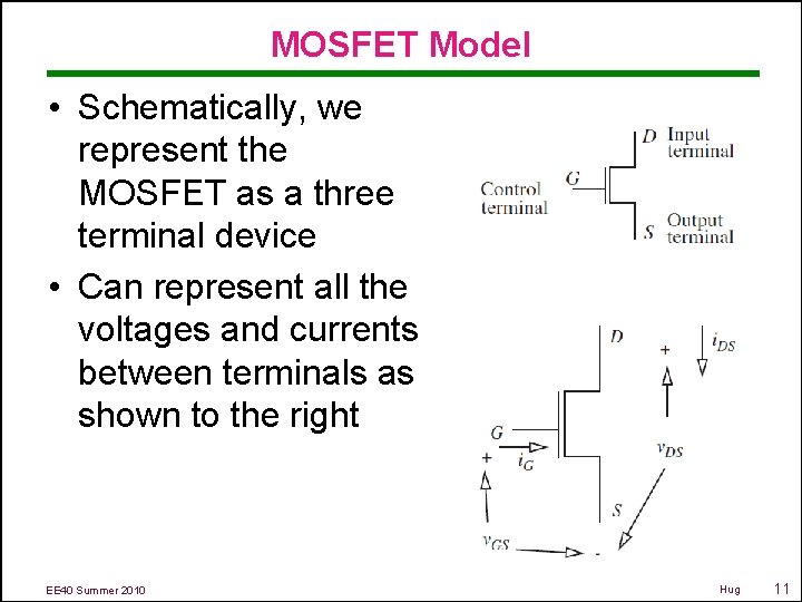
MOSFET Model • Schematically, we represent the MOSFET as a three terminal device • Can represent all the voltages and currents between terminals as shown to the right EE 40 Summer 2010 Hug 11

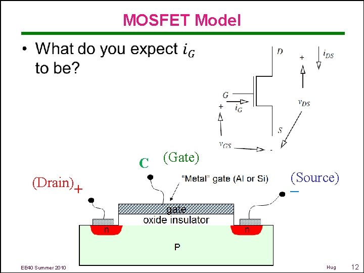
MOSFET Model • C (Drain) EE 40 Summer 2010 + (Gate) (Source) – Hug 12

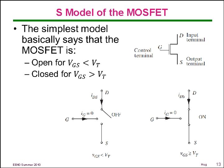
S Model of the MOSFET • EE 40 Summer 2010 Hug 13

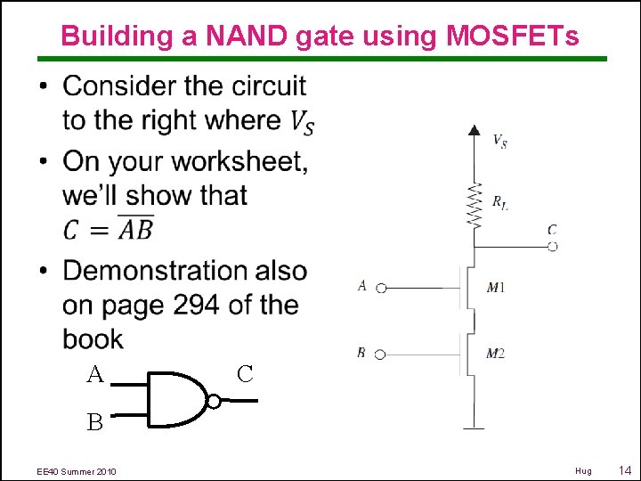
Building a NAND gate using MOSFETs • A C B EE 40 Summer 2010 Hug 14

MOSFET modeling • MOSFET models vary greatly in complexity • For example, an “ON” MOSFET has some effective resistance (not an ideal switch) • We will progressively refine our model of the MOSFET – Will add capacitance later today – If we have time in the next 2 weeks, we will also talk about using MOSFETs as analog amplifiers which will necessitate an even better model EE 40 Summer 2010 Hug 15

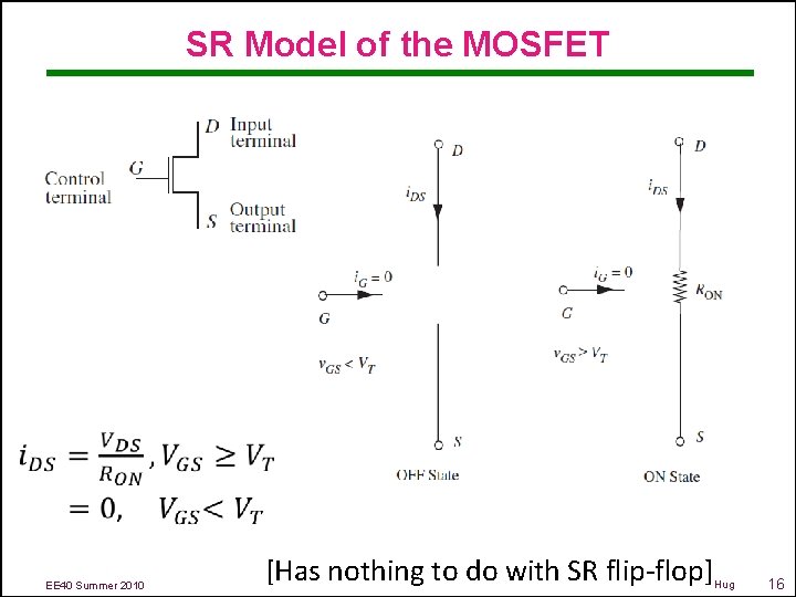
SR Model of the MOSFET EE 40 Summer 2010 [Has nothing to do with SR flip-flop] Hug 16

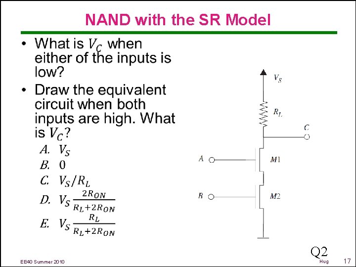
NAND with the SR Model • Q 2 EE 40 Summer 2010 Hug 17

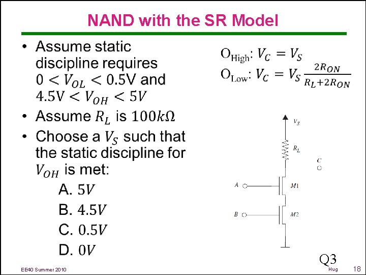
NAND with the SR Model • Q 3 EE 40 Summer 2010 Hug 18

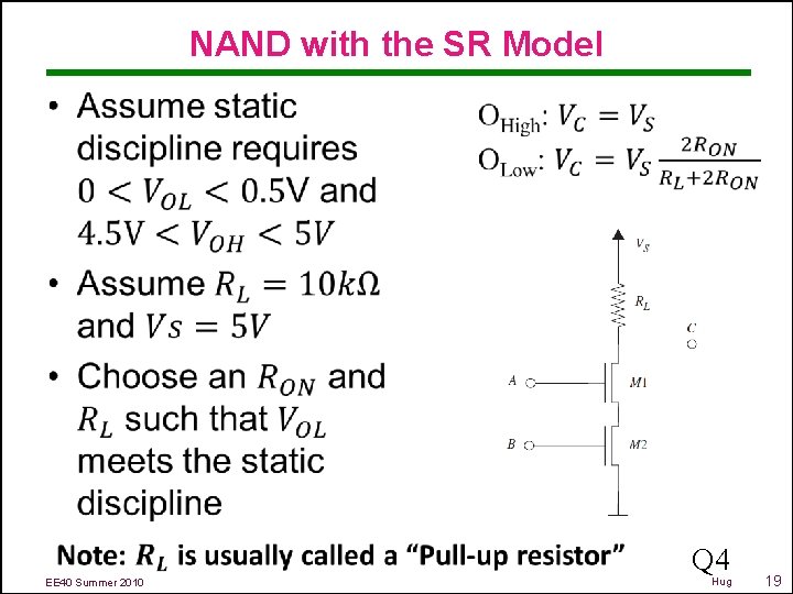
NAND with the SR Model • EE 40 Summer 2010 Q 4 Hug 19

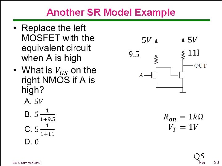
Another SR Model Example • Q 5 EE 40 Summer 2010 Hug 20

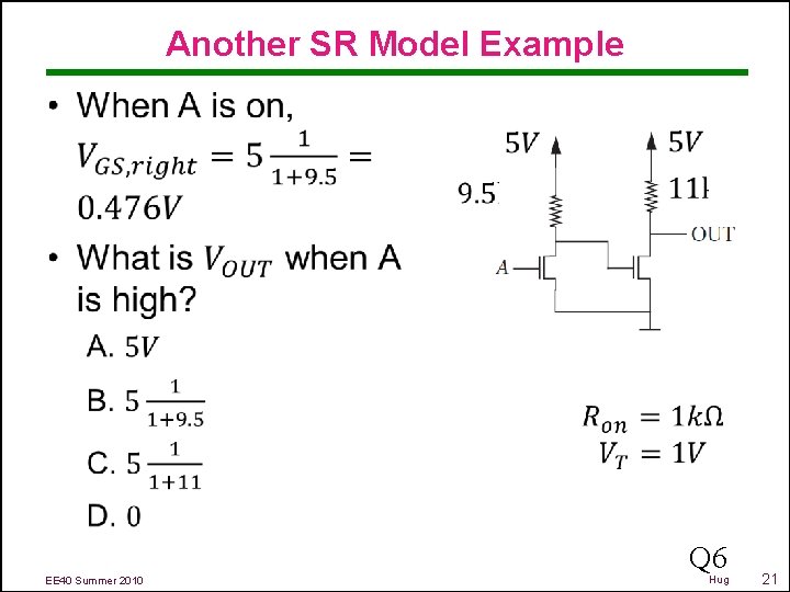
Another SR Model Example • Q 6 EE 40 Summer 2010 Hug 21

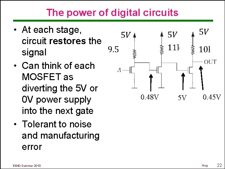
The power of digital circuits • At each stage, circuit restores the signal • Can think of each MOSFET as diverting the 5 V or 0 V power supply into the next gate • Tolerant to noise and manufacturing error EE 40 Summer 2010 0. 48 V 5 V 0. 45 V Hug 22

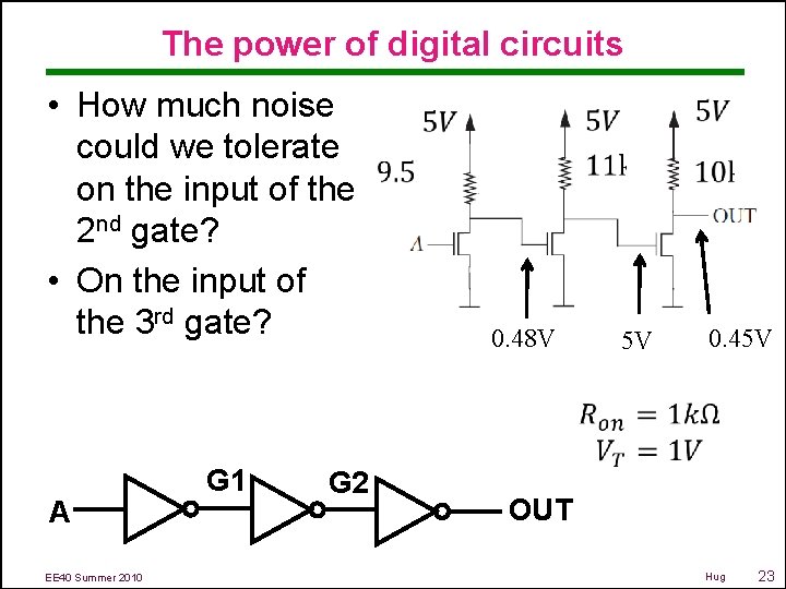
The power of digital circuits • How much noise could we tolerate on the input of the 2 nd gate? • On the input of the 3 rd gate? 0. 48 V 5 V 0. 45 V A EE 40 Summer 2010 G 1 G 2 OUT Hug 23

The power of digital circuits (literally) • Like all circuits, digital circuits consume power • Amount of power will be dependent on state of our MOSFET switches EE 40 Summer 2010 Hug 24

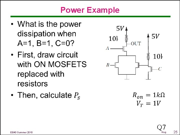
Power Example • Q 7 EE 40 Summer 2010 Hug 25

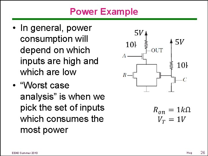
Power Example • In general, power consumption will depend on which inputs are high and which are low • “Worst case analysis” is when we pick the set of inputs which consumes the most power EE 40 Summer 2010 Hug 26

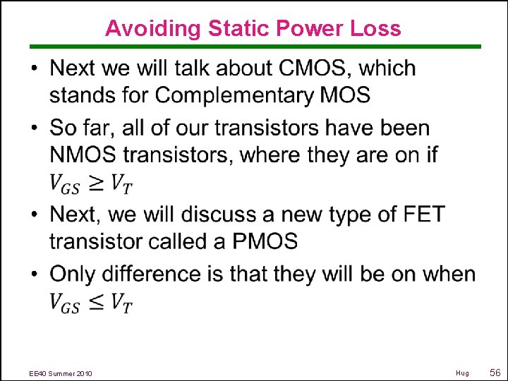
Static Power • Using only NMOS to implement our gates will result in a gate which constantly eats up power – If you wire such a gate up on a breadboard, it will hum along using power all day • Later today, we will see a technique called CMOS to avoid this static power dissipation • But first, let’s discuss delay EE 40 Summer 2010 Hug 27

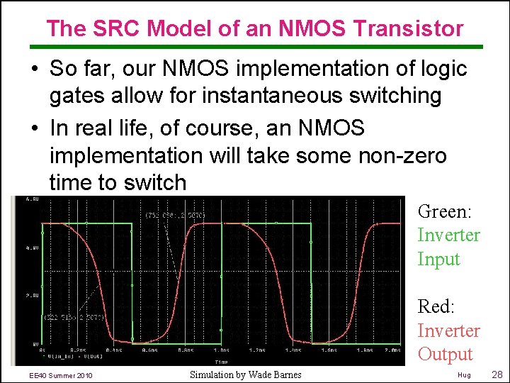
The SRC Model of an NMOS Transistor • So far, our NMOS implementation of logic gates allow for instantaneous switching • In real life, of course, an NMOS implementation will take some non-zero time to switch Green: Inverter Input Red: Inverter Output EE 40 Summer 2010 Simulation by Wade Barnes Hug 28

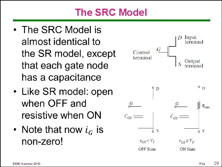
The SRC Model EE 40 Summer 2010 Hug 29

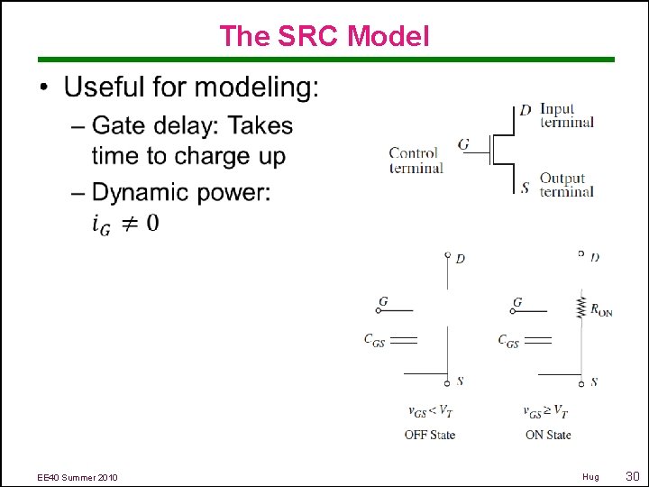
The SRC Model EE 40 Summer 2010 Hug 30

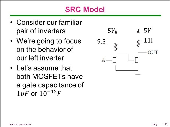
SRC Model • EE 40 Summer 2010 Hug 31

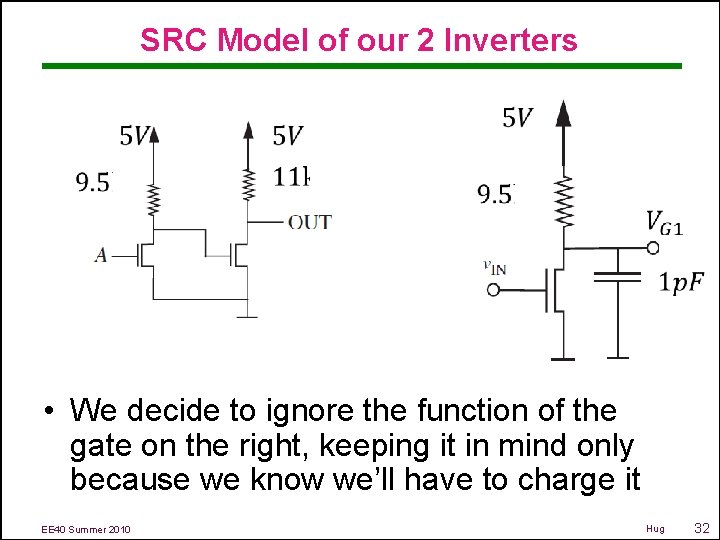
SRC Model of our 2 Inverters • We decide to ignore the function of the gate on the right, keeping it in mind only because we know we’ll have to charge it EE 40 Summer 2010 Hug 32

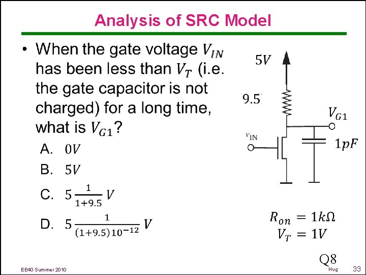
Analysis of SRC Model • Q 8 EE 40 Summer 2010 Hug 33

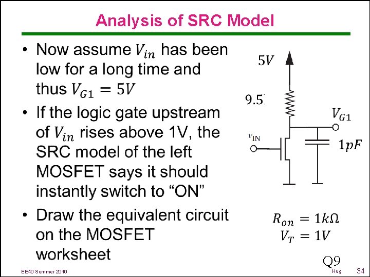
Analysis of SRC Model • Q 9 EE 40 Summer 2010 Hug 34

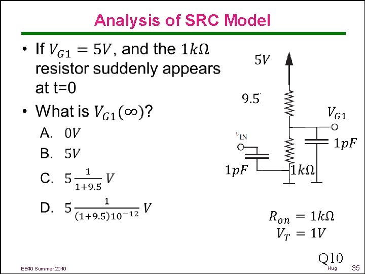
Analysis of SRC Model • Q 10 EE 40 Summer 2010 Hug 35

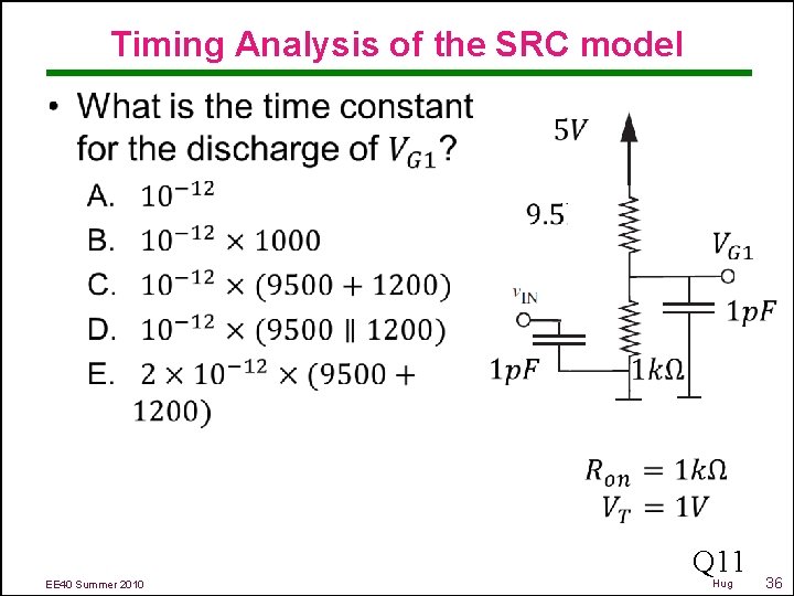
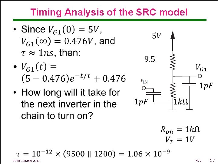
Timing Analysis of the SRC model • Q 11 EE 40 Summer 2010 Hug 36

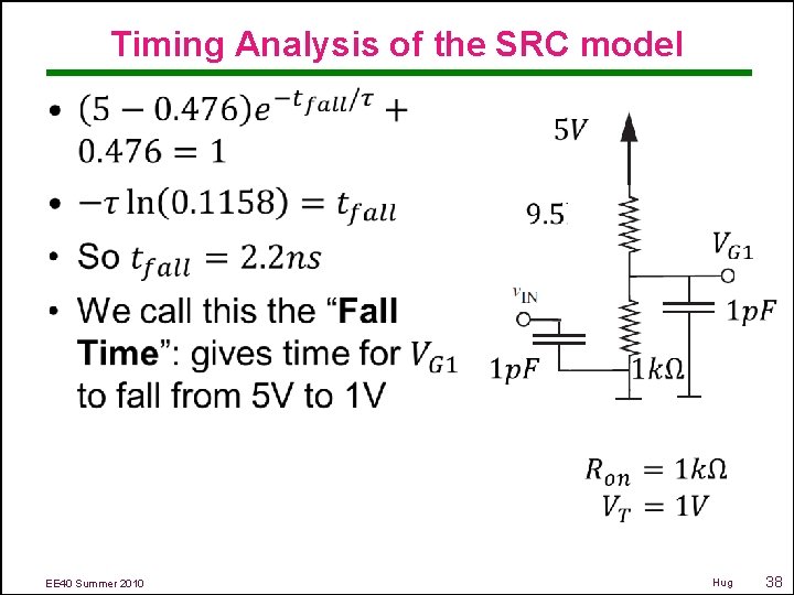
Timing Analysis of the SRC model • EE 40 Summer 2010 Hug 37

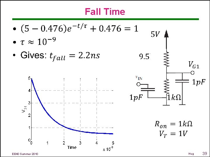
Timing Analysis of the SRC model • EE 40 Summer 2010 Hug 38

Fall Time • EE 40 Summer 2010 Hug 39

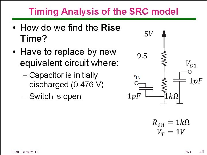
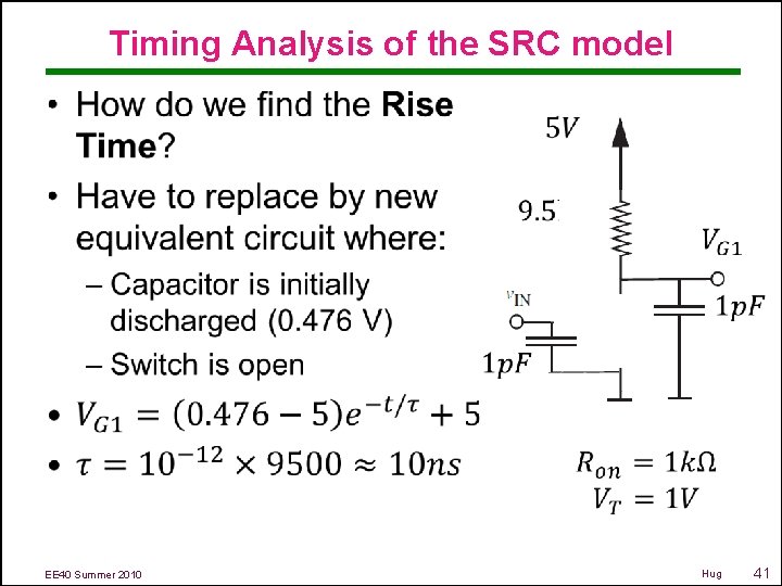
Timing Analysis of the SRC model • How do we find the Rise Time? • Have to replace by new equivalent circuit where: – Capacitor is initially discharged (0. 476 V) – Switch is open EE 40 Summer 2010 Hug 40

Timing Analysis of the SRC model • EE 40 Summer 2010 Hug 41

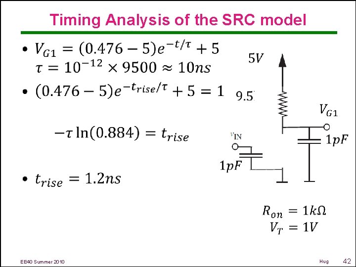
Timing Analysis of the SRC model • EE 40 Summer 2010 Hug 42

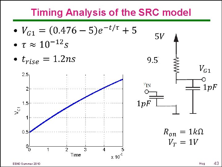
Timing Analysis of the SRC model • EE 40 Summer 2010 Hug 43

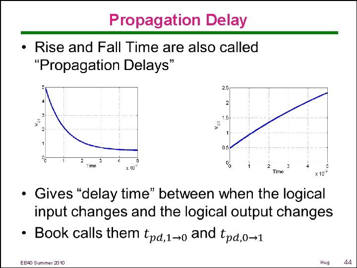
Propagation Delay • EE 40 Summer 2010 Hug 44

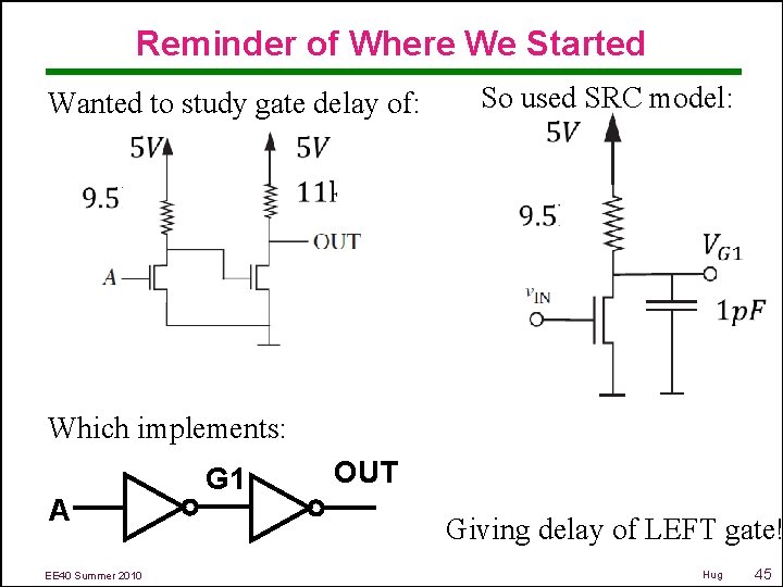
Reminder of Where We Started Wanted to study gate delay of: So used SRC model: Which implements: A EE 40 Summer 2010 G 1 OUT Giving delay of LEFT gate! Hug 45

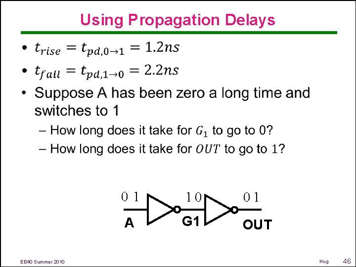
Using Propagation Delays • EE 40 Summer 2010 01 A G 1 OUT Hug 46

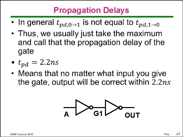
Propagation Delays • A EE 40 Summer 2010 G 1 OUT Hug 47

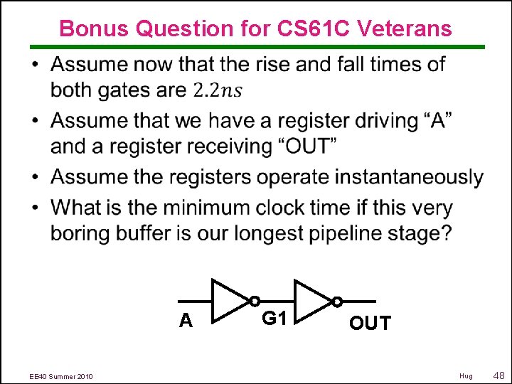
Bonus Question for CS 61 C Veterans • A EE 40 Summer 2010 G 1 OUT Hug 48

• This is where we stopped EE 40 Summer 2010 Hug 49

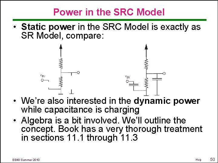
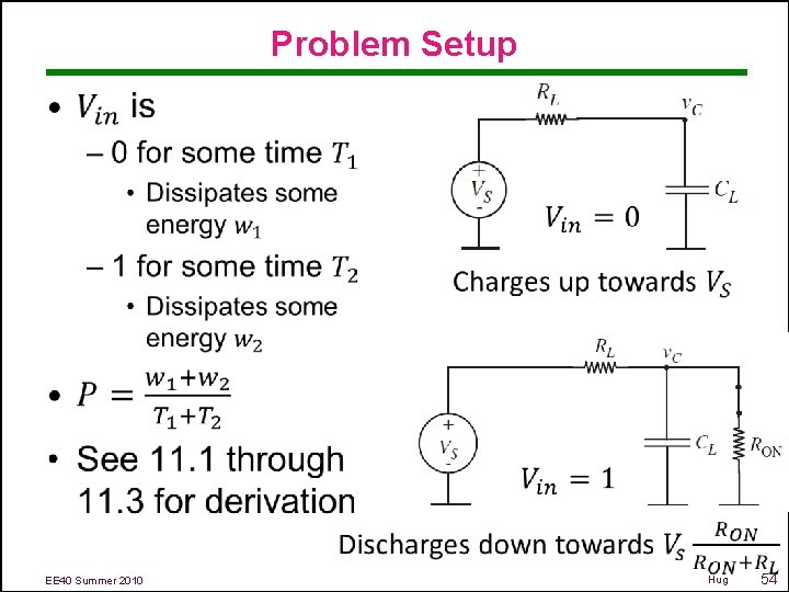
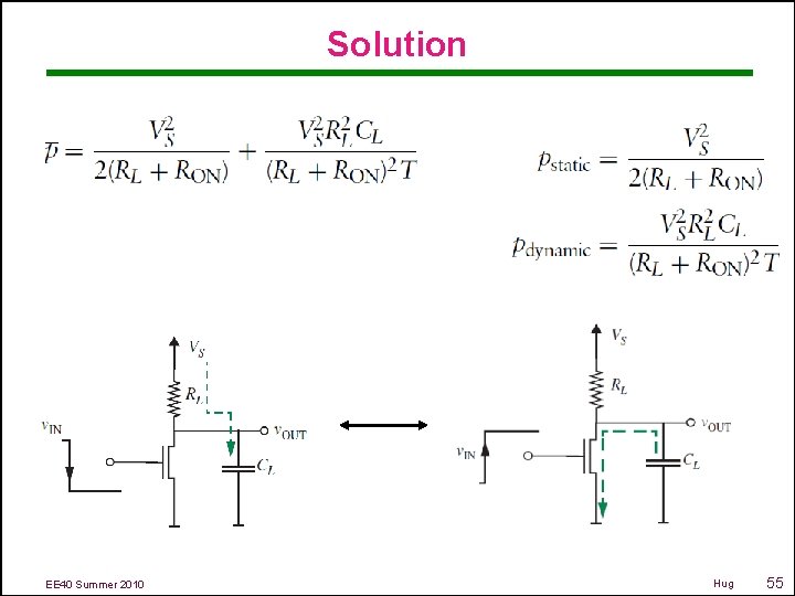
Power in the SRC Model • Static power in the SRC Model is exactly as SR Model, compare: • We’re also interested in the dynamic power while capacitance is charging • Algebra is a bit involved. We’ll outline the concept. Book has a very thorough treatment in sections 11. 1 through 11. 3 EE 40 Summer 2010 Hug 50

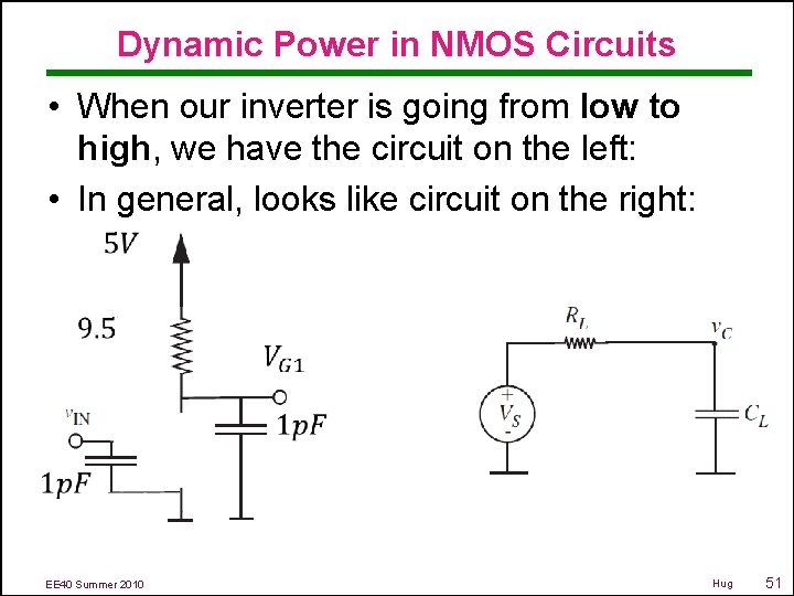
Dynamic Power in NMOS Circuits • When our inverter is going from low to high, we have the circuit on the left: • In general, looks like circuit on the right: EE 40 Summer 2010 Hug 51

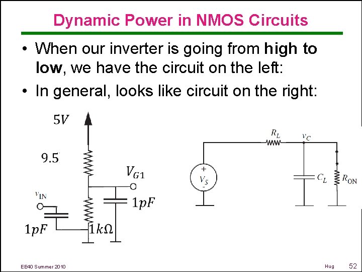
Dynamic Power in NMOS Circuits • When our inverter is going from high to low, we have the circuit on the left: • In general, looks like circuit on the right: EE 40 Summer 2010 Hug 52

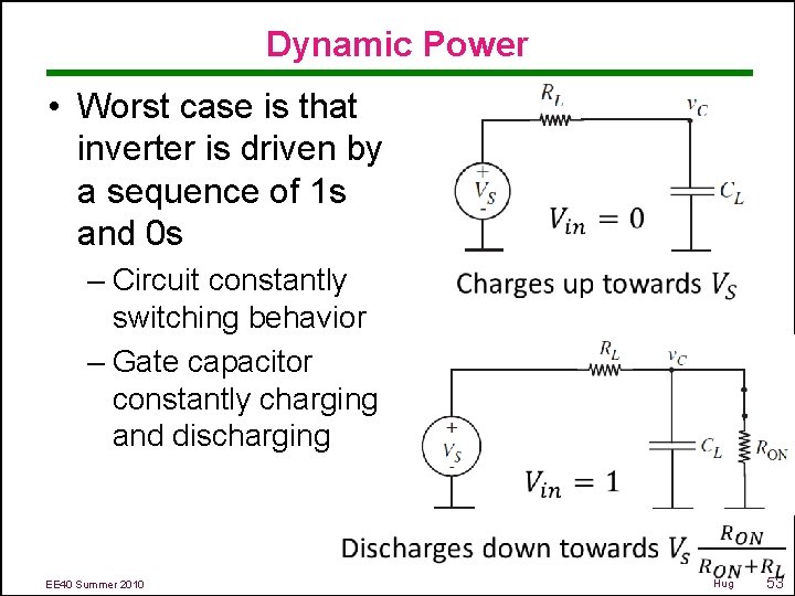
Dynamic Power • Worst case is that inverter is driven by a sequence of 1 s and 0 s – Circuit constantly switching behavior – Gate capacitor constantly charging and discharging EE 40 Summer 2010 Hug 53

Problem Setup • EE 40 Summer 2010 Hug 54

Solution EE 40 Summer 2010 Hug 55

Avoiding Static Power Loss • EE 40 Summer 2010 Hug 56

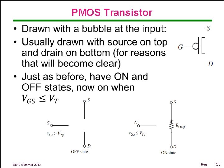
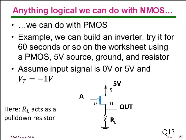
PMOS Transistor • EE 40 Summer 2010 Hug 57

Anything logical we can do with NMOS… • S A G 5 V D OUT RL Q 13 EE 40 Summer 2010 Hug 58

Analysis of PMOS Logic • We could go through and repeat everything we did for NMOS, but it would be almost exactly the same thing • Instead, we’re now going to use NMOS and PMOS in a clever way EE 40 Summer 2010 Hug 59

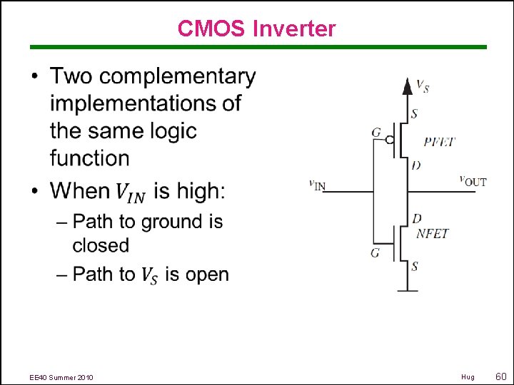
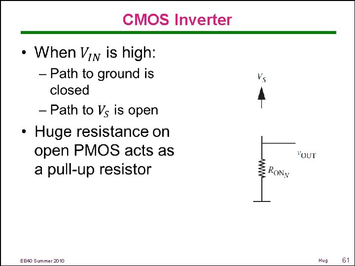
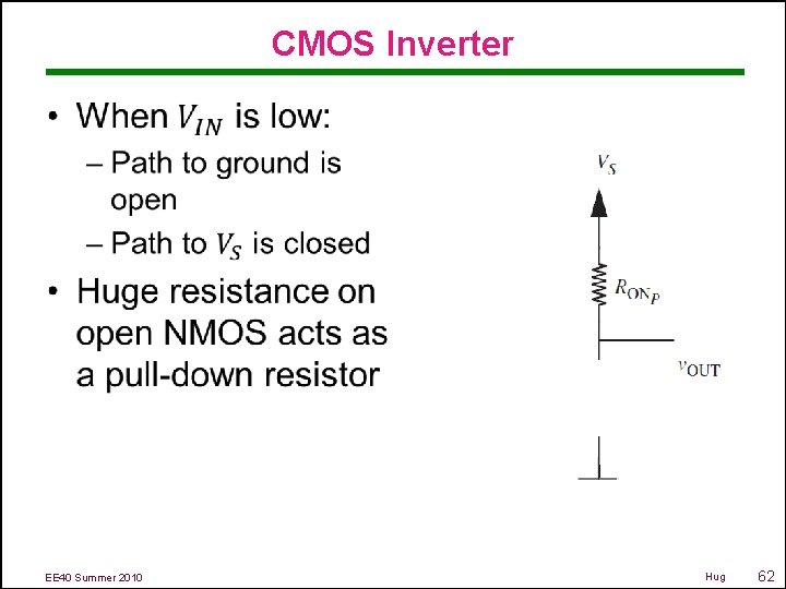
CMOS Inverter • EE 40 Summer 2010 Hug 60

CMOS Inverter • EE 40 Summer 2010 Hug 61

CMOS Inverter • EE 40 Summer 2010 Hug 62

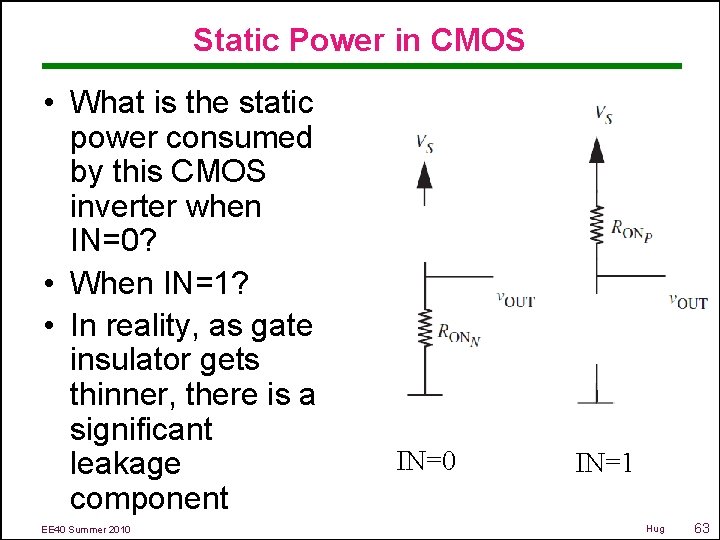
Static Power in CMOS • What is the static power consumed by this CMOS inverter when IN=0? • When IN=1? • In reality, as gate insulator gets thinner, there is a significant leakage component EE 40 Summer 2010 IN=1 Hug 63

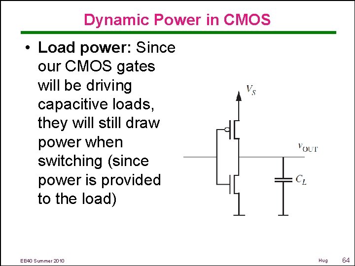
Dynamic Power in CMOS • Load power: Since our CMOS gates will be driving capacitive loads, they will still draw power when switching (since power is provided to the load) EE 40 Summer 2010 Hug 64

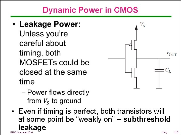
Dynamic Power in CMOS • • Even if timing is perfect, both transistors will at some point be “weakly on” – subthreshold leakage EE 40 Summer 2010 Hug 65

Dynamic Power • These days, subthreshold leakage is a big issue – Thresholds have been reduced to decrease switching times – Reduced thresholds mean leakier MOSFETs • In this class, we won’t analyze this case, but be aware that in the world of digital integrated circuits, it plays a big role EE 40 Summer 2010 Hug 66

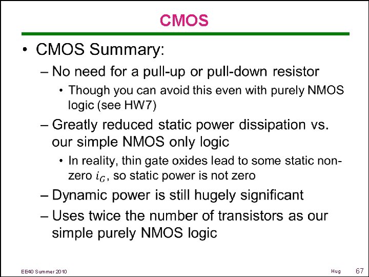
CMOS • EE 40 Summer 2010 Hug 67

Implementation of Complex Gates Using NMOS and CMOS • In class today, we’ve discussed analysis of NMOS and CMOS circuits • Haven’t discussed how to design them • Luckily, it is easy EE 40 Summer 2010 Hug 68

That’s it for today EE 40 Summer 2010 Hug 69

Extra Slides EE 40 Summer 2010 Hug 70

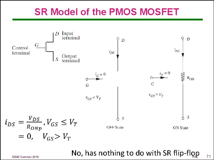
SR Model of the PMOS MOSFET EE 40 Summer 2010 No, has nothing to do with SR flip-flop Hug 71