EE 4 OI 4 Engineering Design Programmable Logic

EE 4 OI 4 Engineering Design Programmable Logic Technology
Evolution of Silicon Chip • We often measure the size of an IC by the number of logic gates or the number of transistors that the IC contains. • Example: 100 k-gate IC: contains equivalent of 100, 000 twoinput NAND gates. • Small-scale integration (SSI) ICs: contains a few (1 to 10) logic gates (often simple gates NANA, NOT, AND) • Medium-scale integration (MSI): increased the range to counters and similar larger scale logic functions • Large-scale integration (LSI): packed even larger logic functions such as the first microprocessor into a single chip • Very large scale integration (VLSI): 64 bit microprocessors with cache memory and floating point arithmetic units (over a million transistor on a single silicon) 2
Evolution of Silicon Chip • Some digital logic ICs are standard parts. • These ICs can be selected from catalog and data books and bought and used in different systems • With the advent of VLSI in the 1980 s engineers began to realize the advantages of designing an IC that was customized or tailored to a particular system or application rather than using standard ICs. 3
Digital logic technology • ICs are made on a thin silicon wafer • The transistors and wiring are made from many layers (between 10 to 15) built on top of one another • The first half-dozen or so layers define the logic cells (AND , OR, Flip-flop). The last half-dozen or so define the wires between the logic cells (mask layer or interconnect) 4

Digital logic technologies. 5
Digital logic technology • In a full-custom IC some (or all) logic cells are customized and all the mask layers are also customized • Example: a microprocessor is a full custom • The designer does not use pre-tested, pre-characterized cells • Why? – No suitable entity cell library available (not fast enough, not small enough, consumes too much power) or no cell library is available (new application) • Full custom ICs are the most expensive to design and manufacture • Design time is long • Fewer and fewer full-custom ICs are being designed because of the above problems 6
Digital logic technology • Traditional integrated circuits chips: perform a fixed operation defined by device manufacturer • Internal functional operation is defined by user: – Application Specific Integrated Circuits (ASIC) – Field Programmable Logic Devices (FPLD) 7
Digital logic technology • ASIC: – Gate arrays – Standard cells • Gate array: an array of pre-manufactured logic cells – A final manufacturing step is required to interconnect the logic cells in a pattern created by the designer to implement a particular design • Standard cell: no fixed internal structure – The manufacturer builds the chip based on the user’s selection of devices from the manufacturer’s standard cell library 8
Digital logic technology • Programmable logic devices (PLDs) are standard ICs that may be configured or programmed to create a part customized to a specific application • Features: – No customized layers or cells – Fast design time 9
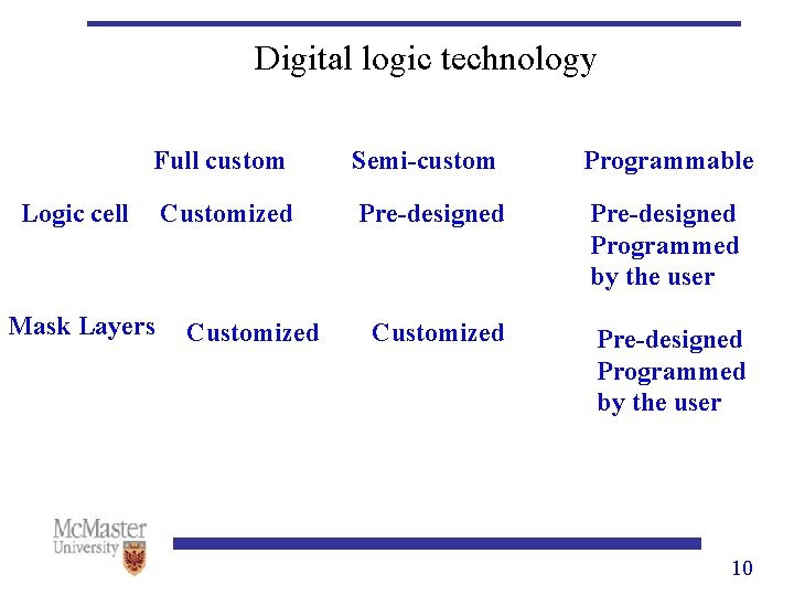
Digital logic technology Full custom Semi-custom Programmable Customized Pre-designed Programmed by the user Logic cell Mask Layers Customized 10
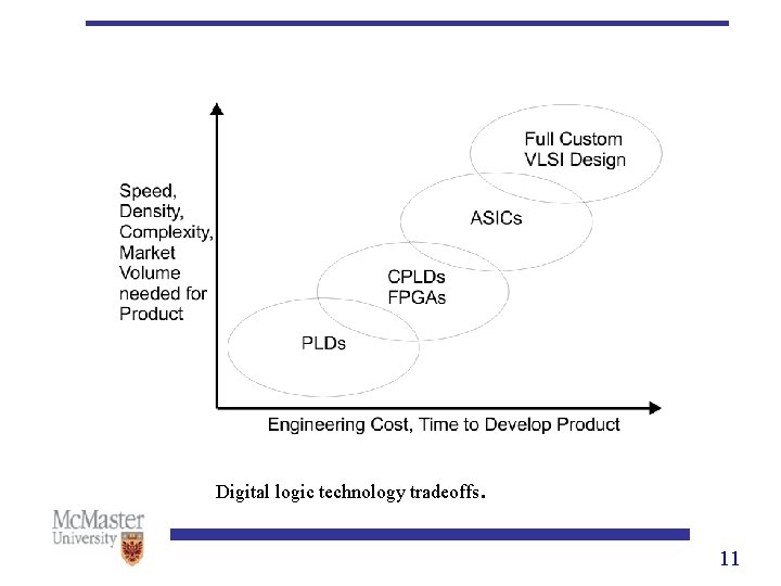
Digital logic technology tradeoffs. 11

Programmable Logic Technology • Simple programmable logic devices (PLDs) such as programmable logic array (PLA) and programmable array logic (PAL) have been in use for over 20 years. • PLA: the idea is that logic functions can be realized in sum-of products form 12
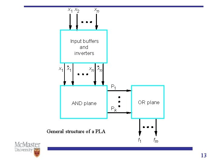
x 1 x 2 xn Input buffers and inverters x 1 xn xn P 1 AND plane OR plane Pk General structure of a PLA f 1 fm 13
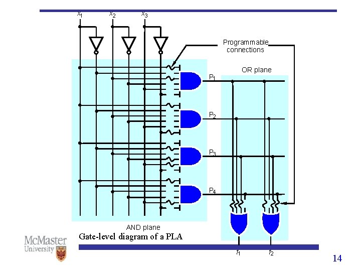
x 1 x 2 x 3 Programmable connections OR plane P 1 P 2 P 3 P 4 AND plane Gate-level diagram of a PLA f 1 f 2 14
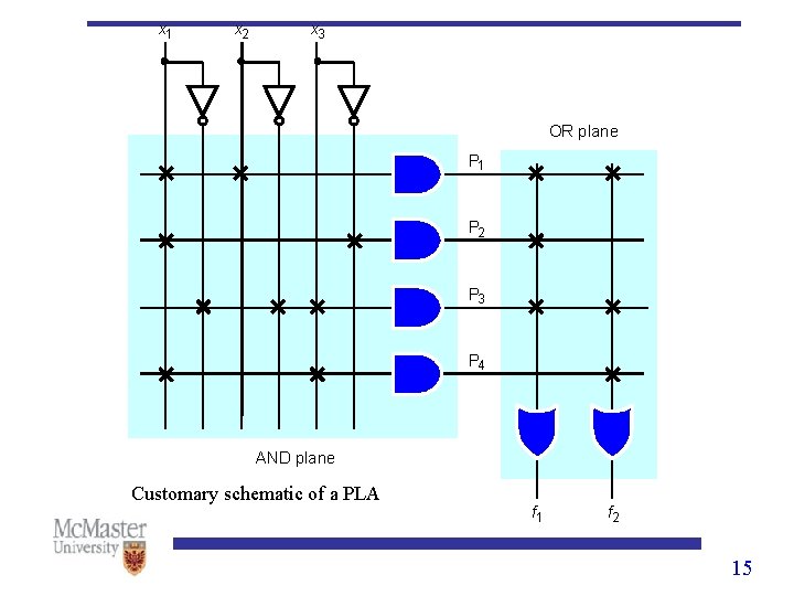
x 1 x 2 x 3 OR plane P 1 P 2 P 3 P 4 AND plane Customary schematic of a PLA f 1 f 2 15
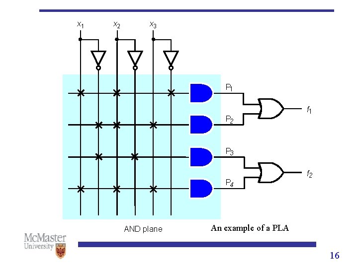
x 1 x 2 x 3 P 1 P 2 f 1 P 3 P 4 AND plane f 2 An example of a PLA 16
Programmable Logic Technology • Programmable connections (switches) are difficult to fabricate and reduce the speed of circuit • In PALs the AND plane is programmable but the OR plane is fixed. • To compensate for reduced flexibility, PALs are manufactured in a range 17

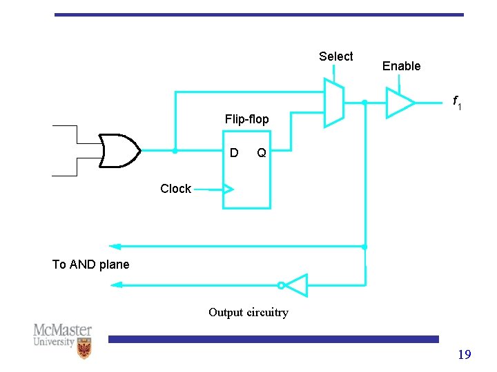
Programmable Logic Technology • On many PLAs and PALs the output of the OR gate is connected to a flip flop whose output can then be feedback as an input into the AND gate array. • This way simple state machines are implemented 18
Select Enable f 1 Flip-flop D Q Clock To AND plane Output circuitry 19
FPLD • CPLDs and FPGAs are the highest density and most advanced programmable logic devices. • These devices are collectively called field programmable logic devices (FPLD). • Characteristics: – None of the mask layers are customized – The core is a regular array of programmable logic cells that can implement combinational as well as sequential logic – A matrix of programmable interconnect surrounds the basic logic cells – Programmable I/O cells • For all but the most time critical design applications, CPLDs and FPGAs have adequate speed (clock range 50 -400 MHz) 20
FPLD • CPLDs and FPGAs typically contain multiple copies of a basic programmable logic element (LE) or logic cell (LC). • Logic element: can implement a network of several logic gates that feed into 1 or 2 flip-flops • Logic elements are arranged in a column or matrix on the chip 21
FPLD • To perform complex operations, logic elements are connected using a programmable interconnection network • Interconnection network contains row and/or column chipwide interconnections. • Interconnection network often contains shorter and faster programmable interconnects limited only to neighboring logic elements 22
FPLD • 1. 2. 3. FPLDs contain: Programmable logic cells Programmable interconnection Programmable I/O cells 23
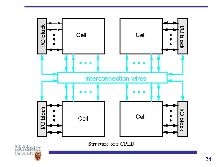
I/O block Cell I/O block Interconnection wires Structure of a CPLD 24

A section of a CPLD 25
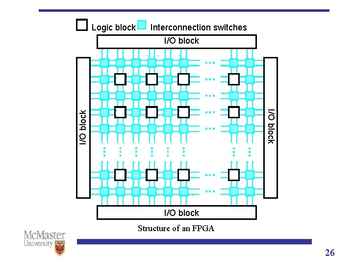
Interconnection switches I/O block Logic block I/O block Structure of an FPGA 26
FPLD • In large FPLDs the clock arrives at different times at different flip flops if it is routed through the chip like a normal signal • The situation in which the clock signal arrives at different times at different flip flops is known as clock skew. • Clock signals in large FPLDs are normally distributed using an internal high speed bus (global clock line) • Using global clock line, clock is distributed to all flip-flops in the device at the same time. 27
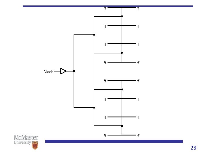
ff ff ff ff Clock Figure 10. 44 An H tree clock distribution network 28
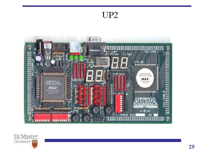
UP 2 29

UP 3 30
Altera MAX 7000 • MAX 7000 is a CPLD family with 600 to 20000 gates. • Configured by an internal electrically erasable programmable read only memory (EEPROM) • Configuration is retained when power is removed • The 7000 family contains from 32 to 256 macrocells. • An individual macrocell contains five programmable AND gates. • The AND/OR network is designed to implement Boolean equations expressed in sum-of-product form. 31

MAX 7000 macrocell. 32
Altera MAX 7000 • Macrocells are combined into groups of 16 called logic array block (LAB) • Input to the AND gates include product terms from other macrocells in the same block or signals from the chip-wide programmable interconnect array (PIA) 33
Altera MAX 7000 • Each I/O pins contains a programmable tri-state output buffer. • An I/O pin can be programmed as input, output with a tri-state driver and tri-state bi-directional. 34
Altera MAX 7000 • If more than five product terms are required, additional product terms are generated using the following methods: 1. Parallel expander: product terms can be shared between macrocells. A macrocell can borrow up to 15 product terms from its neighbors 2. Shared expander: one of the product terms in a macrocell is inverted and fed back to the shared pool of product term. • The inputs to this product term are used in complement form and using De. Morgan’s theorem a sum term is produced. • Since there are 16 macrocells in an LAB, shared logic expander pool has up to 16 terms 35
MAX 7000 CPLD architecture. 36
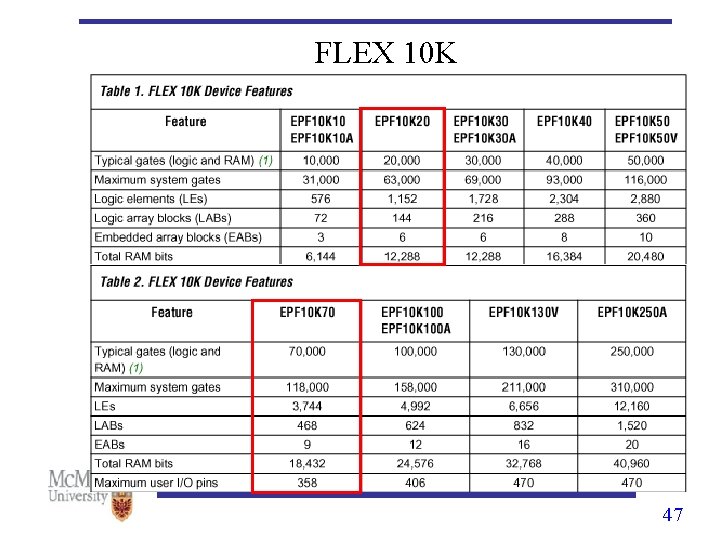
FLEX 10 K • Flex 10 K: an FPGA family with 10, 000 to 250, 000 gates. • Configured by loading internal static random access memory (SRAM). • The configuration is lost whenever power is removed • Gate logic is implemented using a look-up table (LUT) 37
FLEX 10 K • LUT is a high-speed 16 by 1 SRAM. • Four inputs are used to address the LUT’s memory • The truth table for the desired gate network is loaded into the LUT’s SRAM. • A single LUT can model any network of gates with 4 inputs and one output. 38
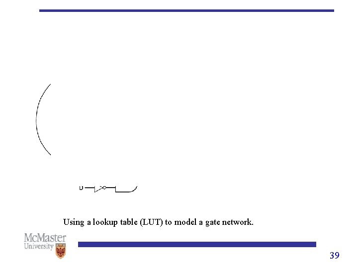
Using a lookup table (LUT) to model a gate network. 39

FLEX 10 K Logic Element (LE). 40
FLEX 10 K • Two dedicated high speed paths are provided in FLEX 10 K: carry chain and cascade chain • They both connect adjacent LEs without using general purpose interconnect path • Carry chain: supports high speed adders and counters (carry forward function between LEs) • Cascade chain can implement functions with a more than 4 inputs. • Adjacent LUTs compute portions of the function in parallel and the cascade chain serially connects the intermediate values • Cascade chain uses logic AND or OR to connect the outputs of adjacent LEs. 41
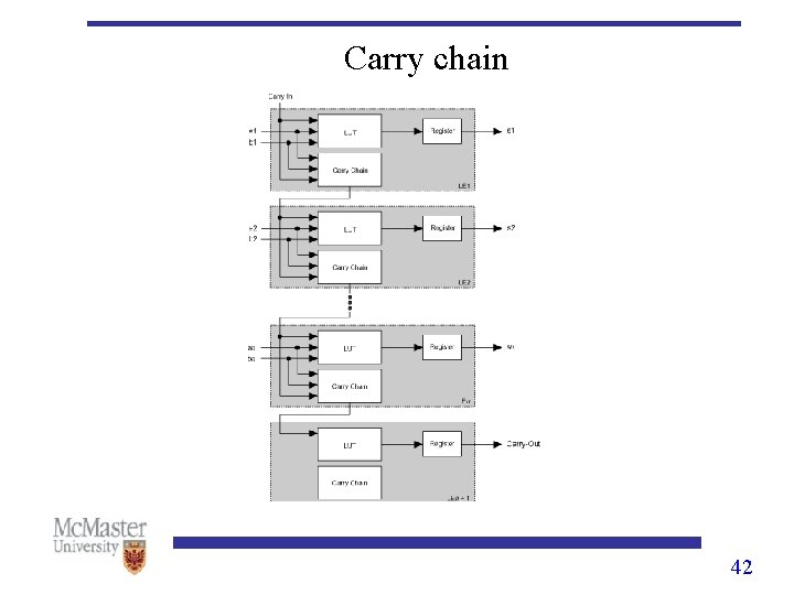
Carry chain 42
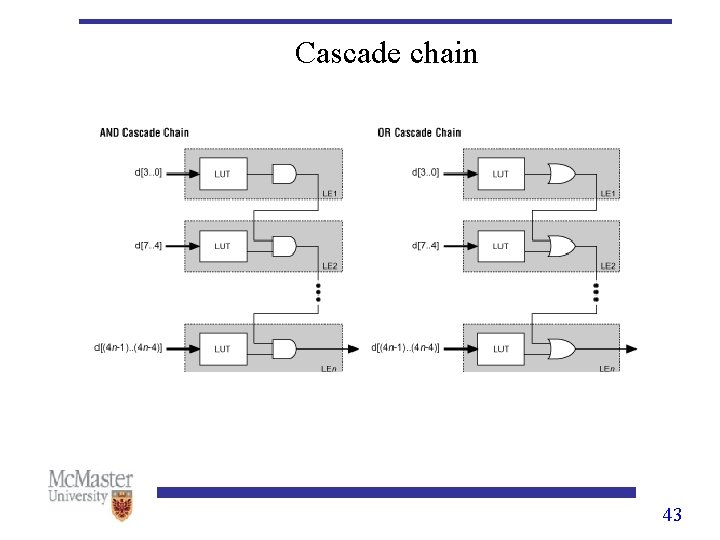
Cascade chain 43
FLEX 10 K Logic Array Block (LAB). 44
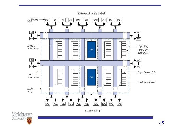
FLEX 10 K CPLD architecture. 45
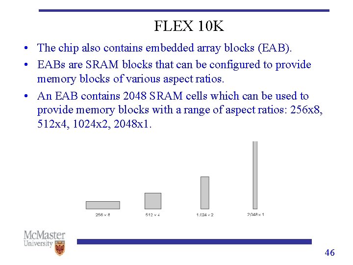
FLEX 10 K • The chip also contains embedded array blocks (EAB). • EABs are SRAM blocks that can be configured to provide memory blocks of various aspect ratios. • An EAB contains 2048 SRAM cells which can be used to provide memory blocks with a range of aspect ratios: 256 x 8, 512 x 4, 1024 x 2, 2048 x 1. 46
FLEX 10 K 47
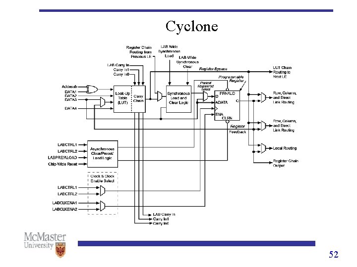
Cyclone • Cyclone: Configured by loading internal static random access memory (SRAM). • The configuration is lost whenever power is removed • Cyclone’s logic array consists of LABs, with 10 Logic Elements (LEs) in each LAB. • An LE is a small unit of logic providing efficient implementation of user logic functions • Cyclone had between 2, 910 to 20, 060 LEs 48
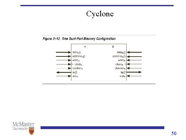
Cyclone • RAM blocks are embedded in Cyclone devices • These blocks are dual-port memory blocks with 4 K bits of memory plus parity (4, 608) • These blocks provide dual-port or single port memory from 1 to 36 bits wide at up to 200 MHz. • These blocks are grouped into columns across the device in between certain LABs • The Cyclone EP 1 C 6 and EP 1 C 12 contain 92 and 239 K bits of embedded RAM 49
Cyclone 50

Cyclone 51
Cyclone 52
Cyclone • • Gate logic is implemented using a look-up table (LUT) The LUT is a high-speed 16 by 1 SRAM Four inputs are used to address the LUT’s memory The truth table for the desired gate network is loaded into the LUT’s SRAM during programming 53
Cyclone • The output of LUT can be fed into a D flip-flop and then to the interconnection network. • More complex gate networks require interconnection with neighboring logic elements. • A logic array block (LAB) is composed of ten logic elements (LE) • Both programmable local LAB and chip-wide row and column interconnects are available • Carry chain are also provided to support faster addition operation 54

Cyclone 55
- Slides: 55