ECO Timing Optimization Using Spare Cells and Technology

- Slides: 41

ECO Timing Optimization Using Spare Cells and Technology Remapping 用預留原件及技術重新映射做 程修改命令的時序最佳化 台灣大學電機 程研究所 陳彥賓 指導教授: 張耀文教授 July 6, 2006 GIEE, NTU The EDA Laboratory 1

Outline ․Introduction & problem formulation ․Previous work and preliminaries ․Algorithm ․Experimental results ․Conclusions GIEE, NTU The EDA Laboratory 2

Outline ․Introduction & problem formulation ․Previous work and preliminaries ․Algorithm ․Experimental results ․Conclusions GIEE, NTU The EDA Laboratory 3

Introduction ․ECO (Engineering Change Order) is usually performed during the chip implementation cycle. ¾ Change the design incrementally. ․When performing ECO to a placed design, change a small portion of netlist to ¾ optimize the chip timing. n ¾ change chip functions. n n GIEE, NTU Functionality is unchanged. Logic bugs. New versions. The EDA Laboratory 4

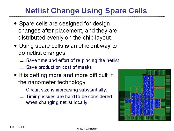
Netlist Change Using Spare Cells ․Spare cells are designed for design changes after placement, and they are distributed evenly on the chip layout. ․Using spare cells is an efficient way to do netlist changes. ¾ ¾ Save time and effort of re-placing the netlist Save production cost of masks ․It is getting more and more difficult in the nanometer technology. ¾ ¾ GIEE, NTU Circuit size is increasing substantially. Timing issues are hard to be considered when changing netlist locally. The EDA Laboratory 5

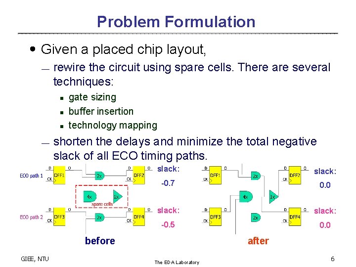
Problem Formulation ․Given a placed chip layout, ¾ rewire the circuit using spare cells. There are several techniques: n n n ¾ gate sizing buffer insertion technology mapping shorten the delays and minimize the total negative slack of all ECO timing paths. slack: -0. 7 0. 0 slack: -0. 5 0. 0 before GIEE, NTU after The EDA Laboratory 6

Outline ․Introduction & problem formulation ․Previous work and preliminaries ․Algorithm ․Experimental results ․Conclusions GIEE, NTU The EDA Laboratory 7

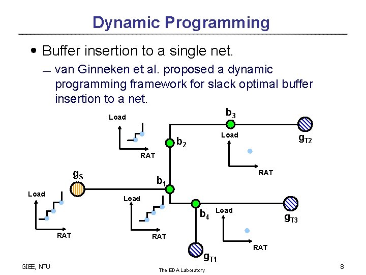
Dynamic Programming ․Buffer insertion to a single net. ¾ van Ginneken et al. proposed a dynamic programming framework for slack optimal buffer insertion to a net. b 3 Load b 2 g. T 2 RAT g. S Load RAT b 1 Load b 4 RAT GIEE, NTU Load g. T 3 RAT g. T 1 The EDA Laboratory RAT 8

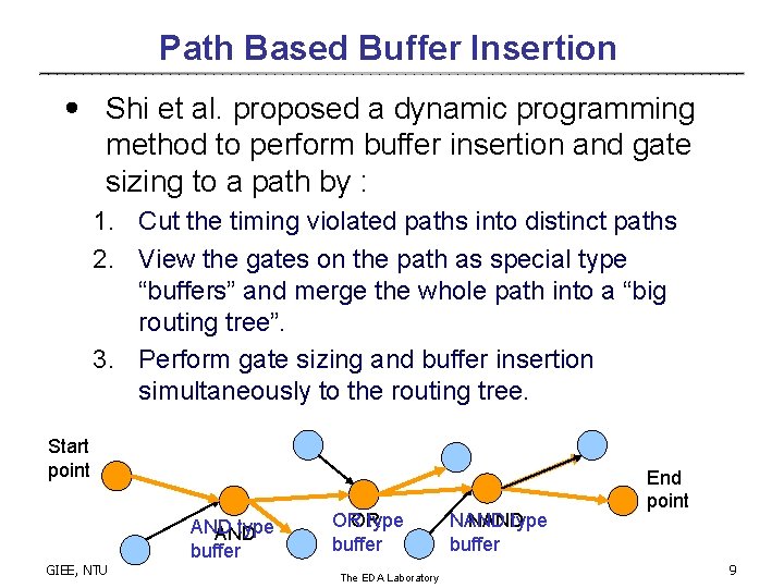
Path Based Buffer Insertion ․ Shi et al. proposed a dynamic programming method to perform buffer insertion and gate sizing to a path by : 1. Cut the timing violated paths into distinct paths 2. View the gates on the path as special type “buffers” and merge the whole path into a “big routing tree”. 3. Perform gate sizing and buffer insertion simultaneously to the routing tree. Start point AND type AND buffer GIEE, NTU OR OR type buffer The EDA Laboratory NAND type buffer End point 9

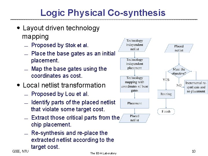
Logic Physical Co-synthesis ․Layout driven technology mapping ¾ ¾ ¾ Proposed by Stok et al. Place the base gates as an initial placement. Map the base gates using the coordinates as cost. ․Local netlist transformation ¾ ¾ GIEE, NTU Proposed by Lou et al. Identify parts of the placed netlist that violate some target cost. Extract those critical parts from the chip placement. Re-synthesis and re-place the extracted netlist according to the target cost. The EDA Laboratory 10

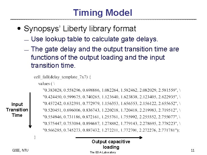
Timing Model ․Synopsys’ Liberty library format ¾ ¾ Use lookup table to calculate gate delays. The gate delay and the output transition time are functions of the output loading and the input transition time. Input Transition Time GIEE, NTU Output capacitive loading The EDA Laboratory 11

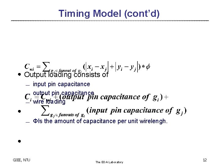
Timing Model (cont’d) ․Output loading consists of ¾ input pin capacitance output pin capacitance wire loading ¾ ΦIs the amount of capacitance per unit wirelengh. ¾ ¾ ․ ․ GIEE, NTU The EDA Laboratory 12

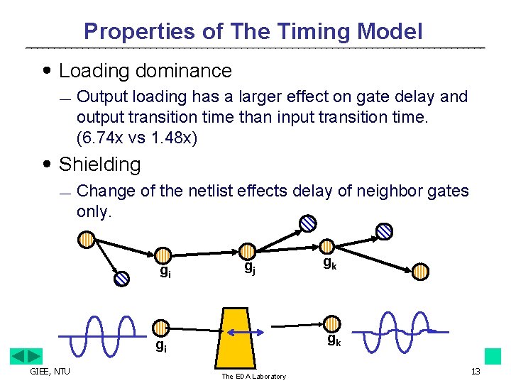
Properties of The Timing Model ․Loading dominance ¾ Output loading has a larger effect on gate delay and output transition time than input transition time. (6. 74 x vs 1. 48 x) ․Shielding ¾ Change of the netlist effects delay of neighbor gates only. gi gj gk gi GIEE, NTU gk The EDA Laboratory 13

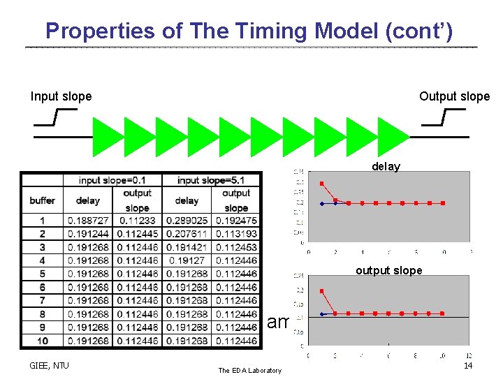
Properties of The Timing Model (cont’) Input slope Output slope delay output slope ․A buffer chain with the same type BUFX 1 GIEE, NTU The EDA Laboratory 14

Outline ․Introduction & problem formulation ․Previous work and preliminaries ․Algorithm ¾ ¾ ¾ Overview Tracing ECO paths Dynamic cost programming Example Timing complexity analysis Technology remapping ․Experimental results ․Conclusions GIEE, NTU The EDA Laboratory 15

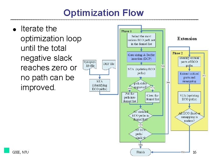
Optimization Flow l Iterate the optimization loop until the total negative slack reaches zero or no path can be improved. GIEE, NTU Extension The EDA Laboratory 16

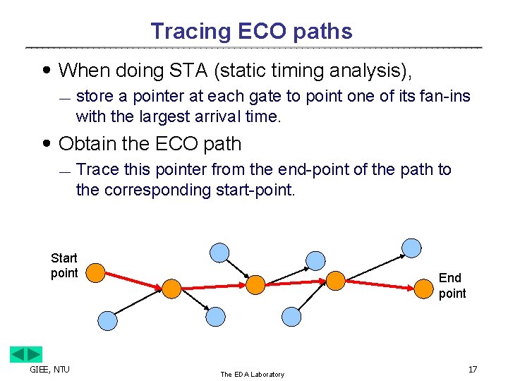
Tracing ECO paths ․When doing STA (static timing analysis), ¾ store a pointer at each gate to point one of its fan-ins with the largest arrival time. ․Obtain the ECO path ¾ Trace this pointer from the end-point of the path to the corresponding start-point. Start point GIEE, NTU End point The EDA Laboratory 17

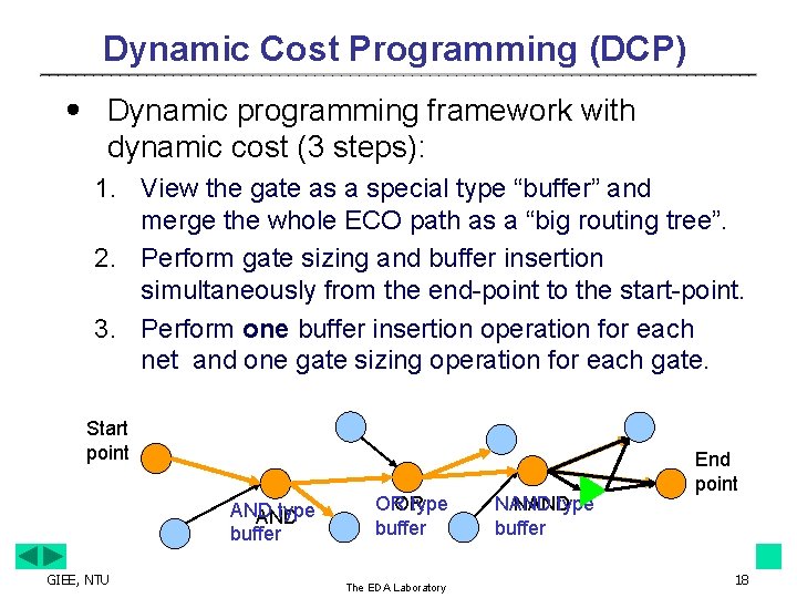
Dynamic Cost Programming (DCP) ․ Dynamic programming framework with dynamic cost (3 steps): 1. View the gate as a special type “buffer” and merge the whole ECO path as a “big routing tree”. 2. Perform gate sizing and buffer insertion simultaneously from the end-point to the start-point. 3. Perform one buffer insertion operation for each net and one gate sizing operation for each gate. Start point AND type AND buffer GIEE, NTU OR OR type buffer The EDA Laboratory NAND type buffer End point 18

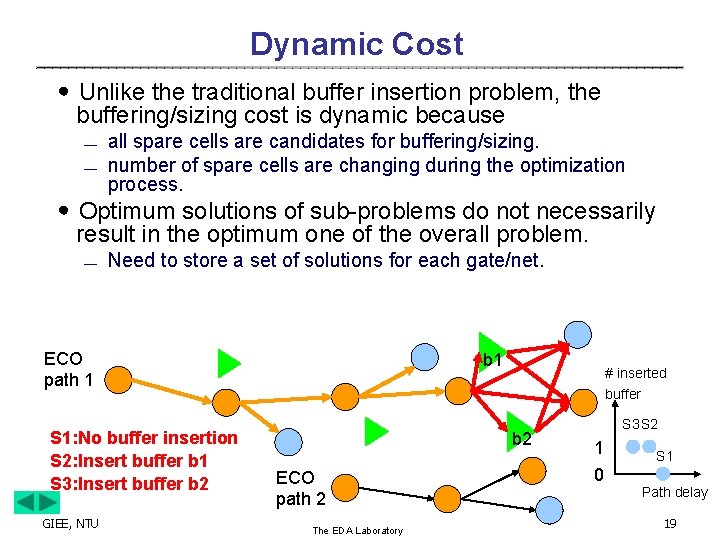
Dynamic Cost ․Unlike the traditional buffer insertion problem, the buffering/sizing cost is dynamic because ¾ ¾ all spare cells are candidates for buffering/sizing. number of spare cells are changing during the optimization process. ․Optimum solutions of sub-problems do not necessarily result in the optimum one of the overall problem. ¾ Need to store a set of solutions for each gate/net. ECO path 1 S 1: No buffer insertion S 2: Insert buffer b 1 S 3: Insert buffer b 2 GIEE, NTU b 1 # inserted buffer b 2 ECO path 2 The EDA Laboratory S 3 S 2 1 0 S 1 Path delay 19

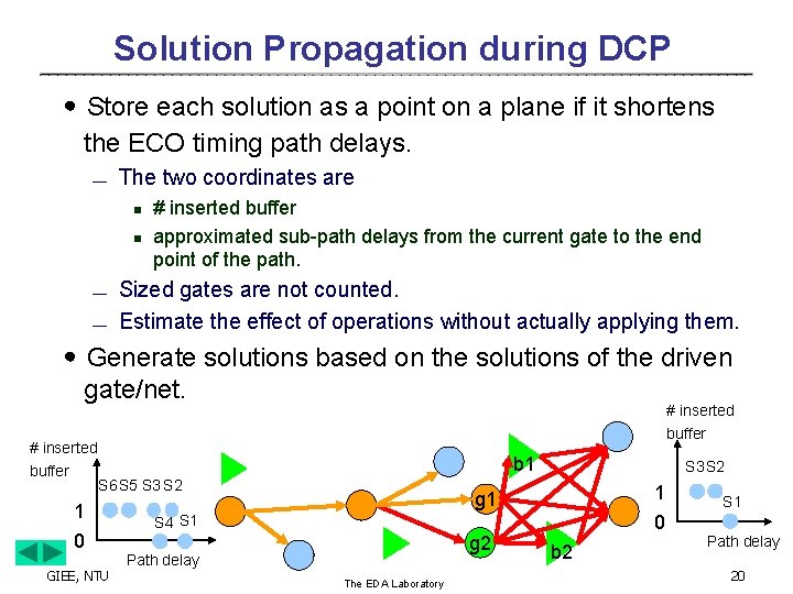
Solution Propagation during DCP ․Store each solution as a point on a plane if it shortens the ECO timing path delays. ¾ The two coordinates are n n ¾ ¾ # inserted buffer approximated sub-path delays from the current gate to the end point of the path. Sized gates are not counted. Estimate the effect of operations without actually applying them. ․Generate solutions based on the solutions of the driven gate/net. # inserted buffer b 1 S 6 S 5 S 3 S 2 1 0 GIEE, NTU S 3 S 2 1 g 1 0 S 4 S 1 g 2 Path delay The EDA Laboratory b 2 S 1 Path delay 20

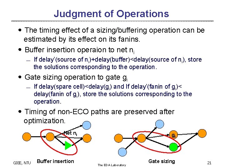
Judgment of Operations ․The timing effect of a sizing/buffering operation can be estimated by its effect on its fanins. ․Buffer insertion operaion to net ni ¾ If delay’(source of ni)+delay(buffer)<delay(source of ni), store the solutions corresponding to the operation. ․Gate sizing operation to gate gi ¾ If delay(spare cell)<delay(gi) and If delay’(fanin of gi)< delay(fanin of gi), store the solutions corresponding to the operation. ․Timing of non-ECO paths are preserved after optimization. Net ni GIEE, NTU Buffer insertion gi The EDA Laboratory Gate sizing 21

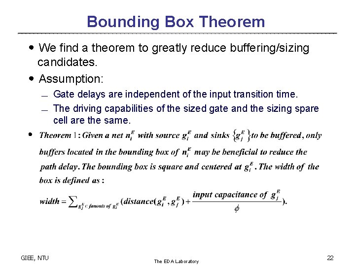
Bounding Box Theorem ․We find a theorem to greatly reduce buffering/sizing candidates. ․Assumption: ¾ ¾ Gate delays are independent of the input transition time. The driving capabilities of the sized gate and the sizing spare cell are the same. ․ GIEE, NTU The EDA Laboratory 22

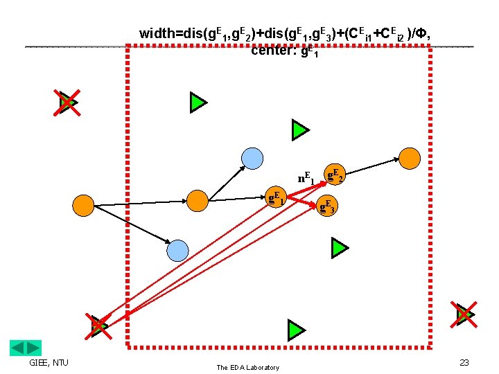
width=dis(g. E 1, g. E 2)+dis(g. E 1, g. E 3)+(CEi 1+CEi 2 )/Φ, center: g. E 1 E n. E 1 g 2 g. E 1 GIEE, NTU The EDA Laboratory g. E 3 23

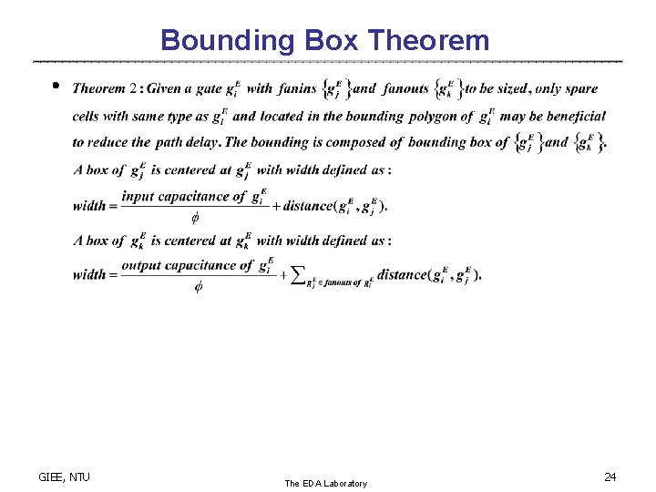
Bounding Box Theorem ․ GIEE, NTU The EDA Laboratory 24

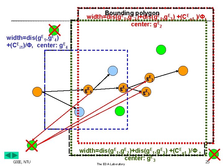
Bounding polygon width=dis(g. E 1, g. E 2)+dis(g. E 1, g. E 3) +(CEo 1 )/Φ, center: g. E 2 width=dis(g. E 1, g. E 4) +(CEi 1)/Φ, center: g. E 4 g. E 2 g. E 4 GIEE, NTU g. E 1 g. E 3 width=dis(g. E 1, g. E 2)+dis(g. E 1, g. E 3) +(CEo 1 )/Φ , center: g. E 3 The EDA Laboratory 25

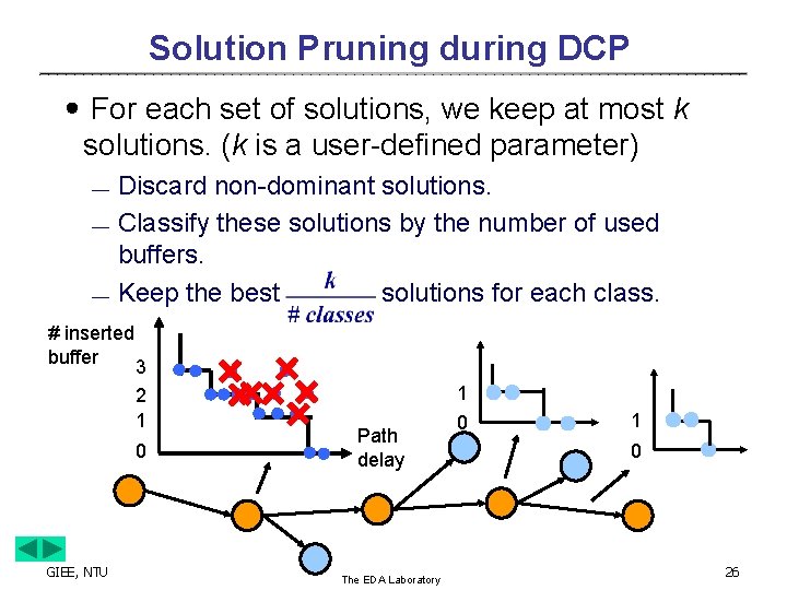
Solution Pruning during DCP ․For each set of solutions, we keep at most k solutions. (k is a user-defined parameter) ¾ ¾ ¾ Discard non-dominant solutions. Classify these solutions by the number of used buffers. Keep the best solutions for each class. # inserted buffer 3 2 1 0 GIEE, NTU 1 Path delay The EDA Laboratory 0 1 0 26

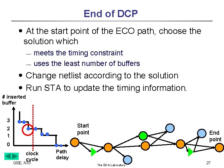
End of DCP ․At the start point of the ECO path, choose the solution which ¾ ¾ meets the timing constraint uses the least number of buffers ․Change netlist according to the solution ․Run STA to update the timing information. # inserted buffer 3 Start point 2 1 End point 0 clock cycle GIEE, NTU Path delay The EDA Laboratory 27

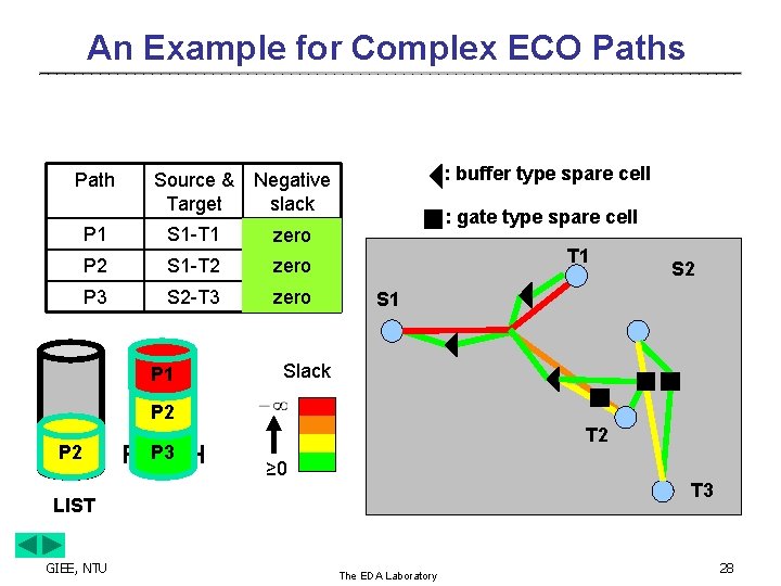
An Example for Complex ECO Paths Path Source & Target Negative slack P 1 S 1 -T 1 large zero P 2 S 1 -T 2 medium small zero P 3 S 2 -T 3 zero small P 1 : buffer type spare cell : gate type spare cell T 1 S 2 S 1 Slack P 2 P 2 P 3 FINISH T 2 ≥ 0 T 3 LIST GIEE, NTU The EDA Laboratory 28

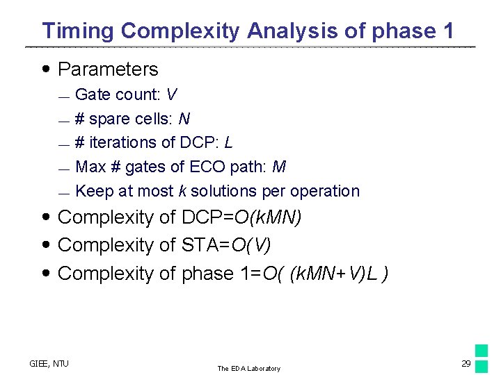
Timing Complexity Analysis of phase 1 ․Parameters ¾ ¾ ¾ Gate count: V # spare cells: N # iterations of DCP: L Max # gates of ECO path: M Keep at most k solutions per operation ․Complexity of DCP=O(k. MN) ․Complexity of STA=O(V) ․Complexity of phase 1=O( (k. MN+V)L ) GIEE, NTU The EDA Laboratory 29

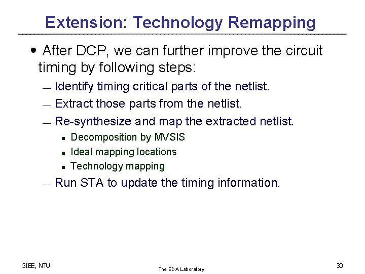
Extension: Technology Remapping ․After DCP, we can further improve the circuit timing by following steps: ¾ ¾ ¾ Identify timing critical parts of the netlist. Extract those parts from the netlist. Re-synthesize and map the extracted netlist. n n n ¾ GIEE, NTU Decomposition by MVSIS Ideal mapping locations Technology mapping Run STA to update the timing information. The EDA Laboratory 30

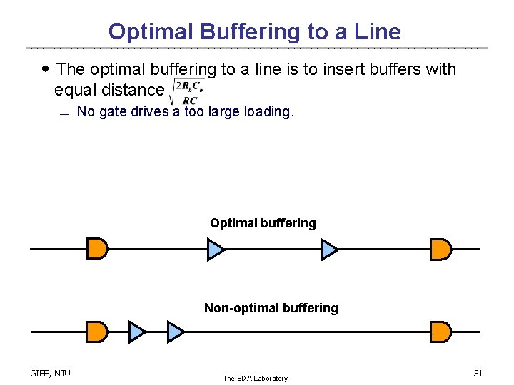
Optimal Buffering to a Line ․The optimal buffering to a line is to insert buffers with equal distance ¾ No gate drives a too large loading. Optimal buffering Non-optimal buffering GIEE, NTU The EDA Laboratory 31

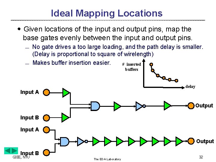
Ideal Mapping Locations ․Given locations of the input and output pins, map the base gates evenly between the input and output pins. ¾ ¾ No gate drives a too large loading, and the path delay is smaller. (Delay is proportional to square of wirelength) Makes buffer insertion easier. # inserted buffers delay Input A Output Input B GIEE, NTU The EDA Laboratory 32

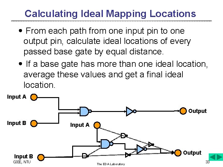
Calculating Ideal Mapping Locations ․From each path from one input pin to one output pin, calculate ideal locations of every passed base gate by equal distance. ․If a base gate has more than one ideal location, average these values and get a final ideal location. Input A Output Input B GIEE, NTU The EDA Laboratory 33

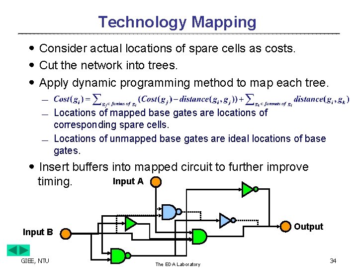
Technology Mapping ․Consider actual locations of spare cells as costs. ․Cut the network into trees. ․Apply dynamic programming method to map each tree. ¾ ¾ ¾ Locations of mapped base gates are locations of corresponding spare cells. Locations of unmapped base gates are ideal locations of base gates. ․Insert buffers into mapped circuit to further improve timing. Input A Output Input B GIEE, NTU The EDA Laboratory 34

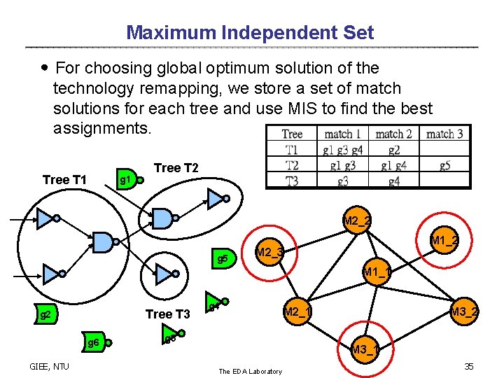
Maximum Independent Set ․For choosing global optimum solution of the technology remapping, we store a set of match solutions for each tree and use MIS to find the best assignments. Tree T 1 g 1 Tree T 2 M 2_2 g 5 M 1_2 M 2_3 M 1_1 Tree T 3 g 2 g 6 GIEE, NTU g 4 M 2_1 M 3_2 g 3 M 3_1 The EDA Laboratory 35

Outline ․Introduction & problem formulation ․Previous work and preliminaries ․Algorithm ․Experimental results ․Conclusions GIEE, NTU The EDA Laboratory 36

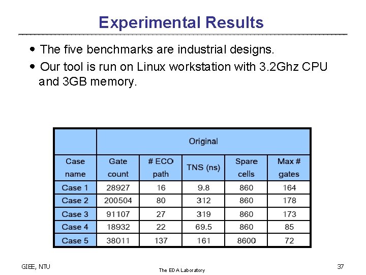
Experimental Results ․The five benchmarks are industrial designs. ․Our tool is run on Linux workstation with 3. 2 Ghz CPU and 3 GB memory. GIEE, NTU The EDA Laboratory 37

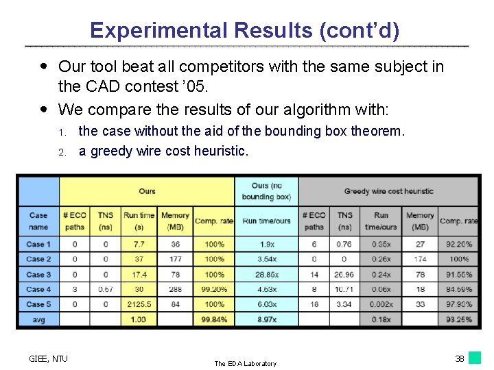
Experimental Results (cont’d) ․ Our tool beat all competitors with the same subject in the CAD contest ’ 05. ․ We compare the results of our algorithm with: 1. 2. GIEE, NTU the case without the aid of the bounding box theorem. a greedy wire cost heuristic. The EDA Laboratory 38

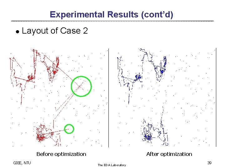
Experimental Results (cont’d) l Layout of Case 2 Before optimization GIEE, NTU After optimization The EDA Laboratory 39

Outline ․Introduction & problem formulation ․Previous work and preliminaries ․Algorithm ․Experimental results ․Conclusions GIEE, NTU The EDA Laboratory 40

Conclusions ․We proposed a dynamic programming method considering dynamic cost to solve the ECO timing optimization problem. ․Functional change considering timing is a tougher work, and we will extend our work in this direction. GIEE, NTU The EDA Laboratory 41