ECECS 552 Single Cycle Datapath Prof Mikko Lipasti
![Load/Store Instructions • lw $1, immed($2) # $1 <= M[SE(immed)+$2] • E. g. MIPS Load/Store Instructions • lw $1, immed($2) # $1 <= M[SE(immed)+$2] • E. g. MIPS](https://slidetodoc.com/presentation_image_h/9d9dd6f435d8dcc4b77ec17e209f390d/image-15.jpg)
- Slides: 20

ECE/CS 552: Single Cycle Datapath © Prof. Mikko Lipasti Lecture notes based in part on slides created by Mark Hill, David Wood, Guri Sohi, John Shen and Jim Smith

Processor Implementation • Forecast – heart of 552 – key to project – Sequential logic design review (brief) – Clock methodology (FSD) – Datapath – 1 CPI • Single instruction, 2’s complement, unsigned • Next: – – Control Multiple cycle implementation (information only) Microprogramming Exceptions

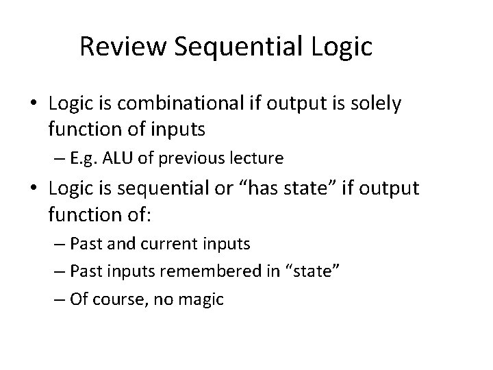
Review Sequential Logic • Logic is combinational if output is solely function of inputs – E. g. ALU of previous lecture • Logic is sequential or “has state” if output function of: – Past and current inputs – Past inputs remembered in “state” – Of course, no magic

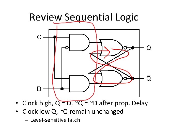
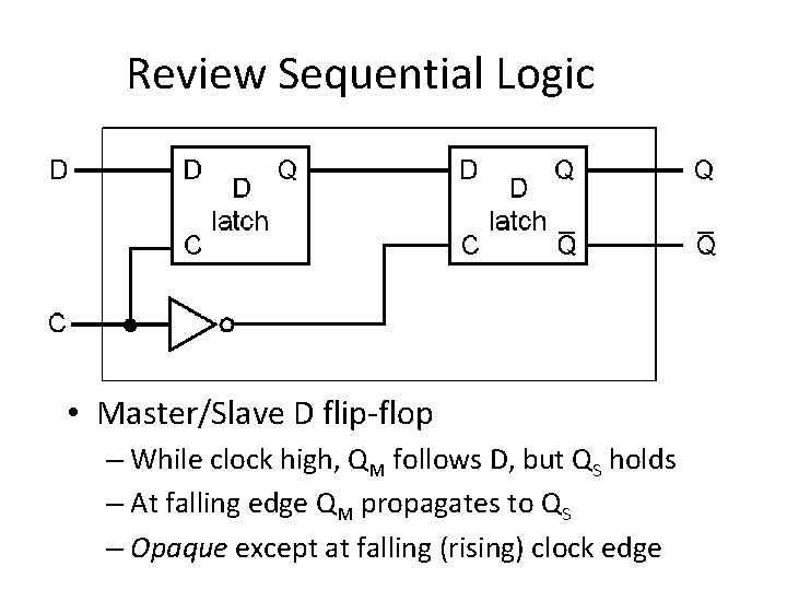
Review Sequential Logic • Clock high, Q = D, ~Q = ~D after prop. Delay • Clock low Q, ~Q remain unchanged – Level-sensitive latch

Review Sequential Logic • Master/Slave D flip-flop – While clock high, QM follows D, but QS holds – At falling edge QM propagates to QS – Opaque except at falling (rising) clock edge

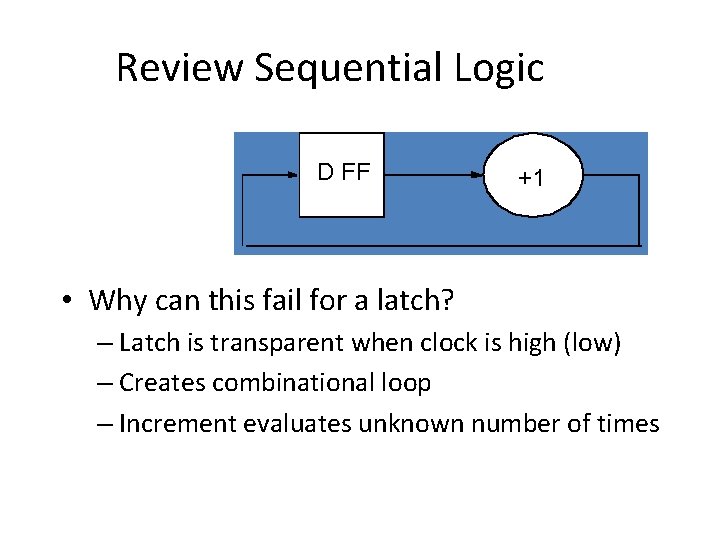
Review Sequential Logic D FF +1 • Why can this fail for a latch? – Latch is transparent when clock is high (low) – Creates combinational loop – Increment evaluates unknown number of times

Clocking Methology • Motivation – Design data and control without considering clock • Use Fully Synchronous Design (FSD) – Just a convention to simplify design process – Restricts design freedom – Eliminates complexity, can guarantee timing correctness – Not really feasible in real designs: off-chip I/O – Even in ECE 554 you will violate FSD

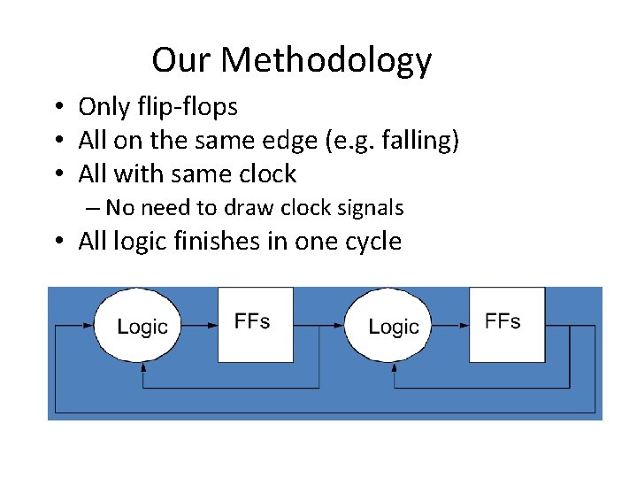
Our Methodology • Only flip-flops • All on the same edge (e. g. falling) • All with same clock – No need to draw clock signals • All logic finishes in one cycle

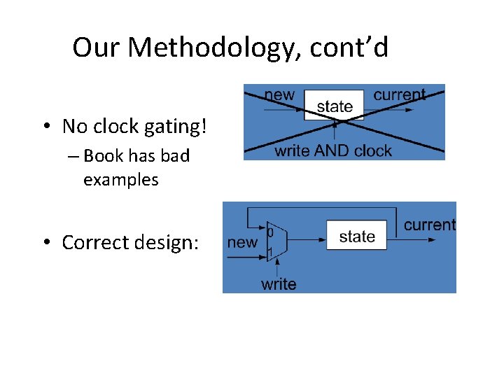
Our Methodology, cont’d • No clock gating! – Book has bad examples • Correct design:

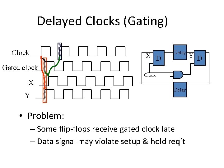
Delayed Clocks (Gating) Clock X D Delay Gated clock Clock X Delay Y • Problem: – Some flip-flops receive gated clock late – Data signal may violate setup & hold req’t Y D

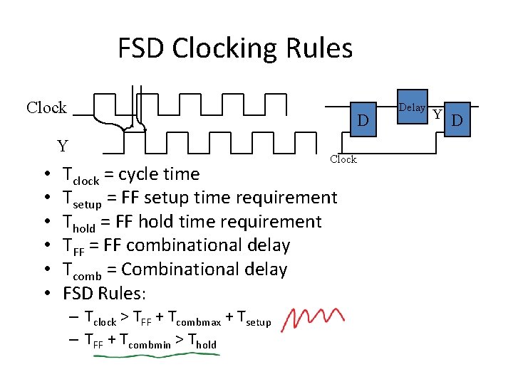
FSD Clocking Rules Clock D Y • • • Clock Tclock = cycle time Tsetup = FF setup time requirement Thold = FF hold time requirement TFF = FF combinational delay Tcomb = Combinational delay FSD Rules: – Tclock > TFF + Tcombmax + Tsetup – TFF + Tcombmin > Thold Delay Y D

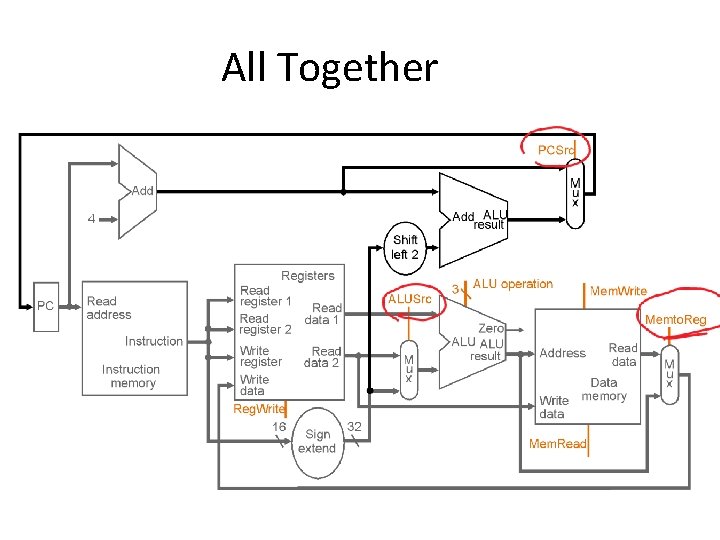
Datapath – 1 CPI • Assumption: get whole instruction done in one long cycle • Instructions: – and, lw, sw, & beq • To do – For each instruction type – Putting it all together

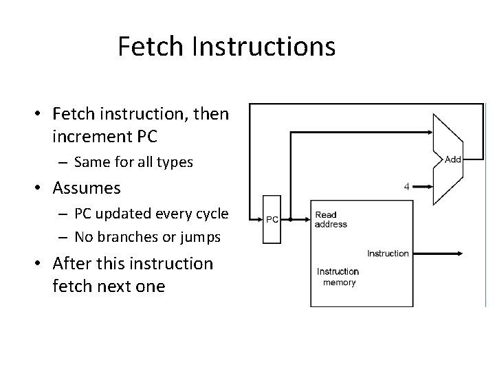
Fetch Instructions • Fetch instruction, then increment PC – Same for all types • Assumes – PC updated every cycle – No branches or jumps • After this instruction fetch next one

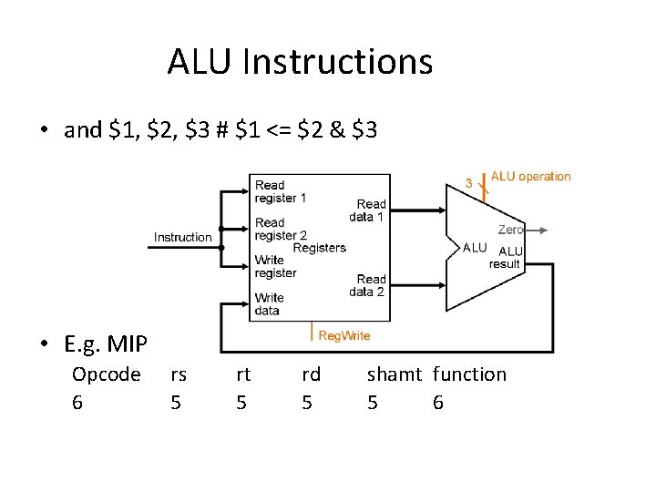
ALU Instructions • and $1, $2, $3 # $1 <= $2 & $3 • E. g. MIPS R-format Opcode 6 rs 5 rt 5 rd 5 shamt function 5 6
![LoadStore Instructions lw 1 immed2 1 MSEimmed2 E g MIPS Load/Store Instructions • lw $1, immed($2) # $1 <= M[SE(immed)+$2] • E. g. MIPS](https://slidetodoc.com/presentation_image_h/9d9dd6f435d8dcc4b77ec17e209f390d/image-15.jpg)
Load/Store Instructions • lw $1, immed($2) # $1 <= M[SE(immed)+$2] • E. g. MIPS I-format: Opcode 6 rt 5 immed 16

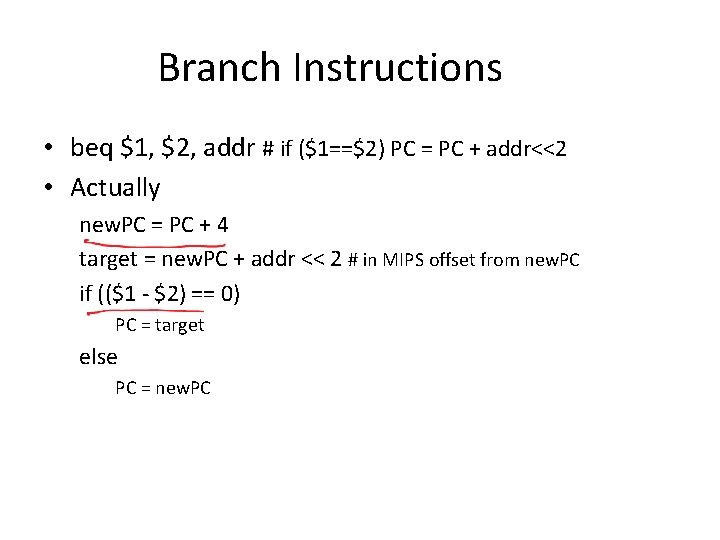
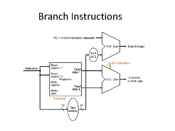
Branch Instructions • beq $1, $2, addr # if ($1==$2) PC = PC + addr<<2 • Actually new. PC = PC + 4 target = new. PC + addr << 2 # in MIPS offset from new. PC if (($1 - $2) == 0) PC = target else PC = new. PC

Branch Instructions

All Together

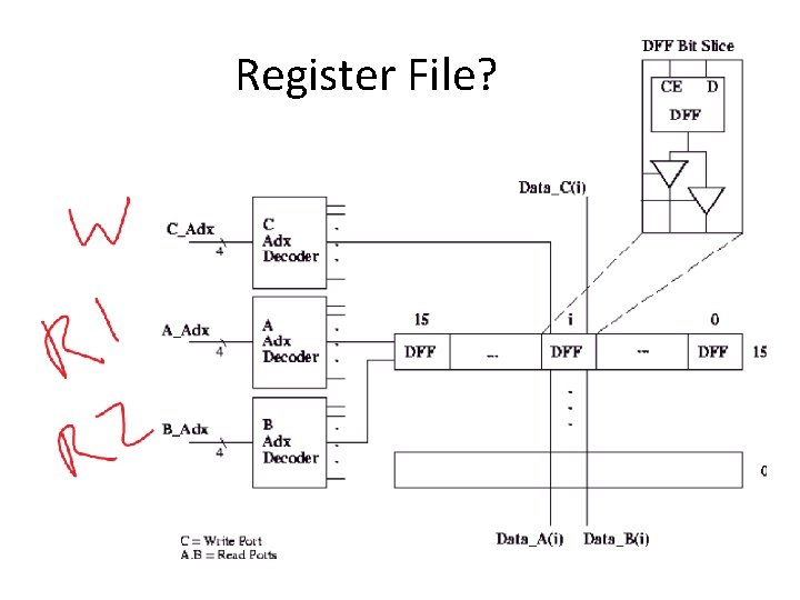
Register File?

Summary • Sequential logic design review (brief) • Clock methodology (FSD) • Datapath – 1 CPI – ALU, lw, sw, beq instructions