ECE 679 Digital Systems Engineering Patrick Chiang Office



- Slides: 30

ECE 679: Digital Systems Engineering Patrick Chiang Office Hours: 1 -2 PM Mon-Thurs GLSN 100

Class Introductions • Who am I • Who are you

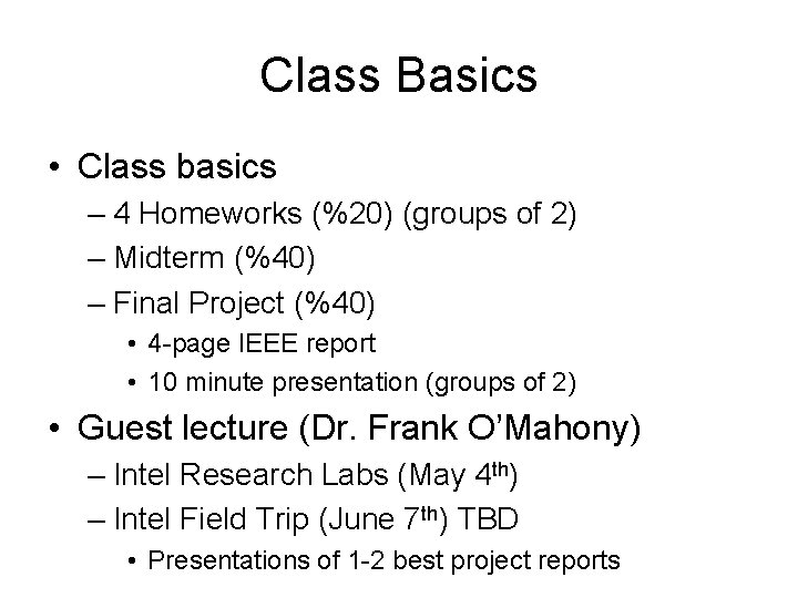
Class Basics • Class basics – 4 Homeworks (%20) (groups of 2) – Midterm (%40) – Final Project (%40) • 4 -page IEEE report • 10 minute presentation (groups of 2) • Guest lecture (Dr. Frank O’Mahony) – Intel Research Labs (May 4 th) – Intel Field Trip (June 7 th) TBD • Presentations of 1 -2 best project reports

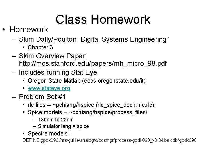
• Homework Class Homework – Skim Dally/Poulton “Digital Systems Engineering” • Chapter 3 – Skim Overview Paper: http: //mos. stanford. edu/papers/mh_micro_98. pdf – Includes running Stat Eye • Oregon State Matlab (eecs. oregonstate. edu/it) • www. stateye. org – Problem Set #1 • rlc files -- ~pchiang/hspice (rlc_spice_deck; rlc) • Spice models -- ~pchiang/hspice/process_files/ – 130 nm to 22 nm – Simulator lang = spice • Spectre models – DEFINE gpdk 090 /nfs/guille/analog/c/cdsmgr/process/gpdk 090_v 3. 8/libs. cdb/gpdk 090


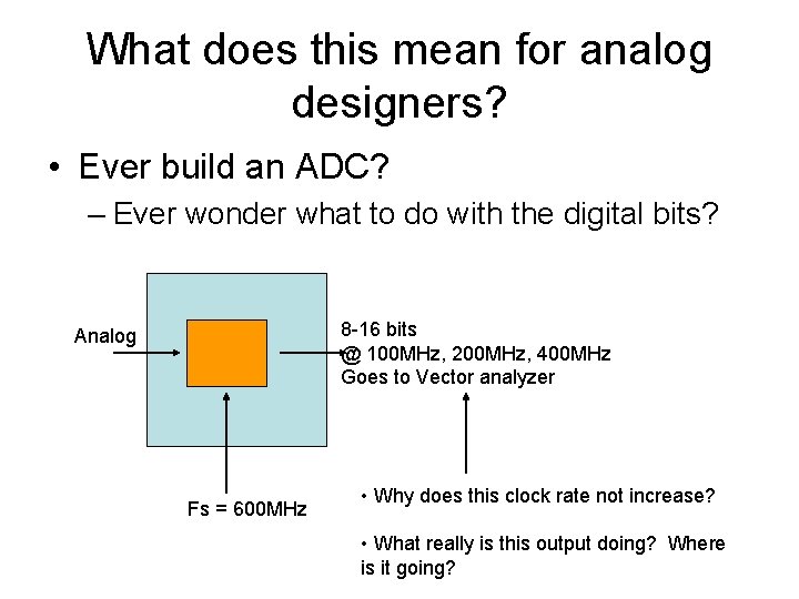
What does this mean for analog designers? • Ever build an ADC? – Ever wonder what to do with the digital bits? 8 -16 bits @ 100 MHz, 200 MHz, 400 MHz Goes to Vector analyzer Analog Fs = 600 MHz • Why does this clock rate not increase? • What really is this output doing? Where is it going?


Brief Summary • Introduction to the area – Why serial links are important – What are the current technology trends/limitations

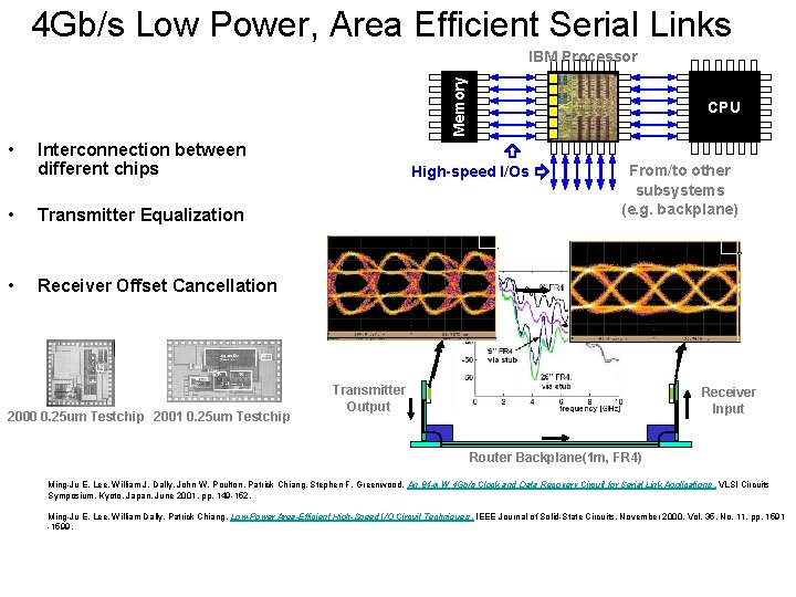
4 Gb/s Low Power, Area Efficient Serial Links Memory IBM Processor • Interconnection between different chips • Transmitter Equalization • Receiver Offset Cancellation 2000 0. 25 um Testchip 2001 0. 25 um Testchip CPU High-speed I/Os CPU From/to other subsystems (e. g. backplane) Transmitter Output Receiver Input Router Backplane(1 m, FR 4) Ming-Ju E. Lee, William J. Dally, John W. Poulton, Patrick Chiang, Stephen F. Greenwood. An 84 -m. W 4 Gb/s Clock and Data Recovery Circuit for Serial Link Applications. VLSI Circuits Symposium, Kyoto, Japan, June 2001, pp. 149 -152. Ming-Ju E. Lee, William Dally, Patrick Chiang. Low-Power Area-Efficient High-Speed I/O Circuit Techniques. IEEE Journal of Solid-State Circuits, November 2000, Vol. 35, No. 11, pp. 1591 -1599.

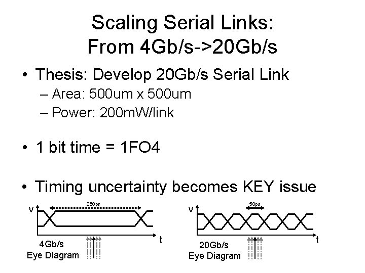
Scaling Serial Links: From 4 Gb/s->20 Gb/s • Thesis: Develop 20 Gb/s Serial Link – Area: 500 um x 500 um – Power: 200 m. W/link • 1 bit time = 1 FO 4 • Timing uncertainty becomes KEY issue v 4 Gb/s Eye Diagram 250 ps v t 20 Gb/s Eye Diagram 50 ps t

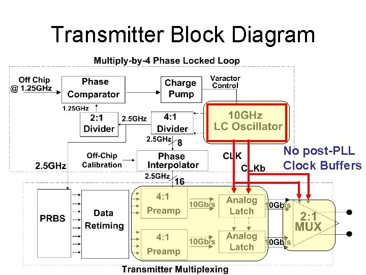
Transmitter Block Diagram No post-PLL Clock Buffers

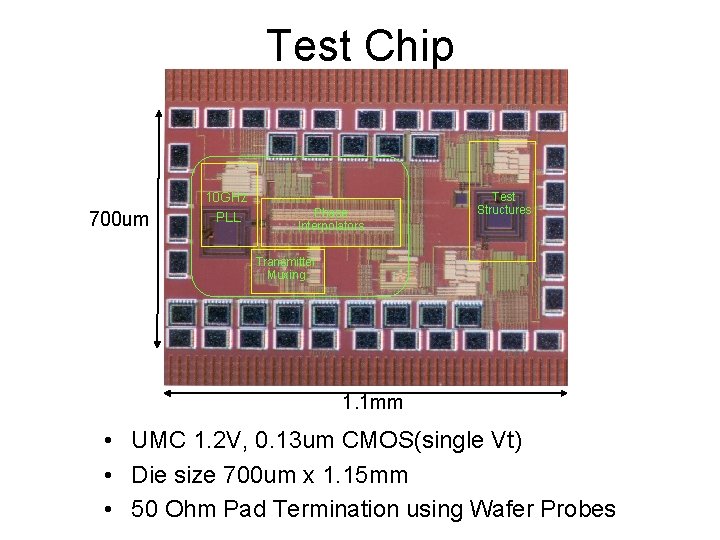
Test Chip Test Interface 700 um 10 GHz PRBS Check PLL DLL TX Phase Interpolators Clock Transmitter Muxing RX Test Structures Recovery PRBS Gen 1. 1 mm • UMC 1. 2 V, 0. 13 um CMOS(single Vt) • Die size 700 um x 1. 15 mm • 50 Ohm Pad Termination using Wafer Probes

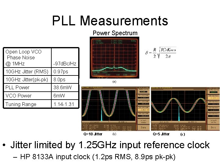
PLL Measurements Power Spectrum Open Loop VCO Phase Noise @ 1 MHz -97 d. Bc/Hz 10 GHz Jitter (RMS) 0. 97 ps 10 GHz Jitter(pk-pk) 8. 0 ps PLL Power 38. 6 m. W VCO Power 6 m. W Tuning Range 1. 14 -1. 31 Q=10 Jitter Q=5 Jitter (c) • Jitter limited by 1. 25 GHz input reference clock – HP 8133 A input clock (1. 2 ps RMS, 8. 9 ps pk-pk)

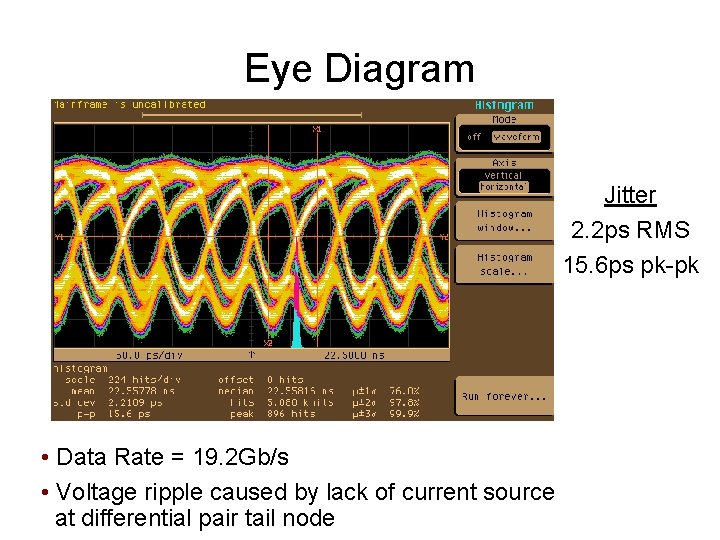
Eye Diagram Jitter 2. 2 ps RMS 15. 6 ps pk-pk • Data Rate = 19. 2 Gb/s • Voltage ripple caused by lack of current source at differential pair tail node

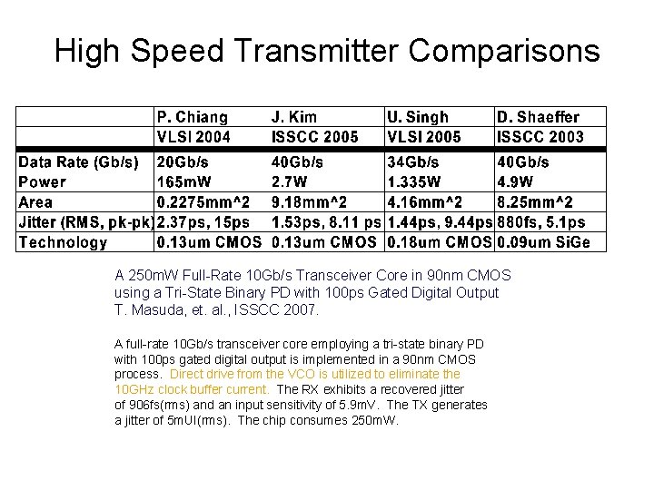
High Speed Transmitter Comparisons A 250 m. W Full-Rate 10 Gb/s Transceiver Core in 90 nm CMOS using a Tri-State Binary PD with 100 ps Gated Digital Output T. Masuda, et. al. , ISSCC 2007. A full-rate 10 Gb/s transceiver core employing a tri-state binary PD with 100 ps gated digital output is implemented in a 90 nm CMOS process. Direct drive from the VCO is utilized to eliminate the 10 GHz clock buffer current. The RX exhibits a recovered jitter of 906 fs(rms) and an input sensitivity of 5. 9 m. V. The TX generates a jitter of 5 m. UI(rms). The chip consumes 250 m. W.

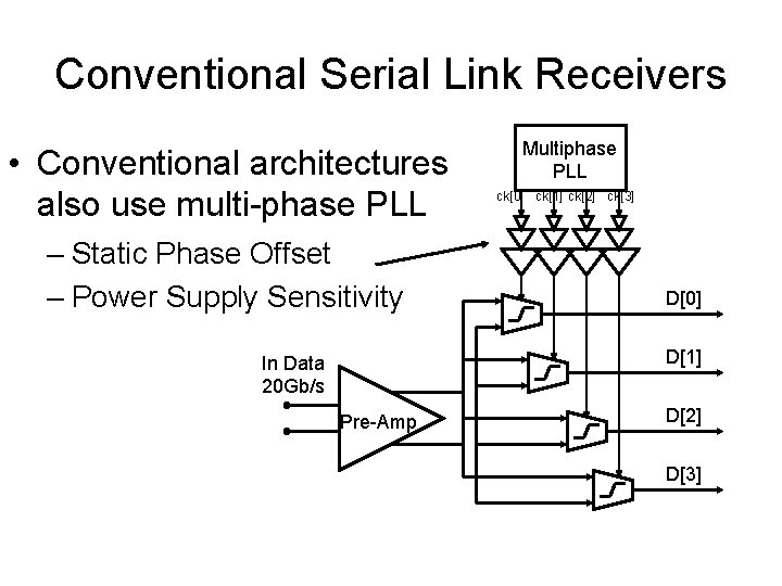
Conventional Serial Link Receivers • Conventional architectures also use multi-phase PLL – Static Phase Offset – Power Supply Sensitivity Multiphase PLL ck[0] ck[1] ck[2] ck[3] D[0] D[1] In Data 20 Gb/s Pre-Amp D[2] D[3]

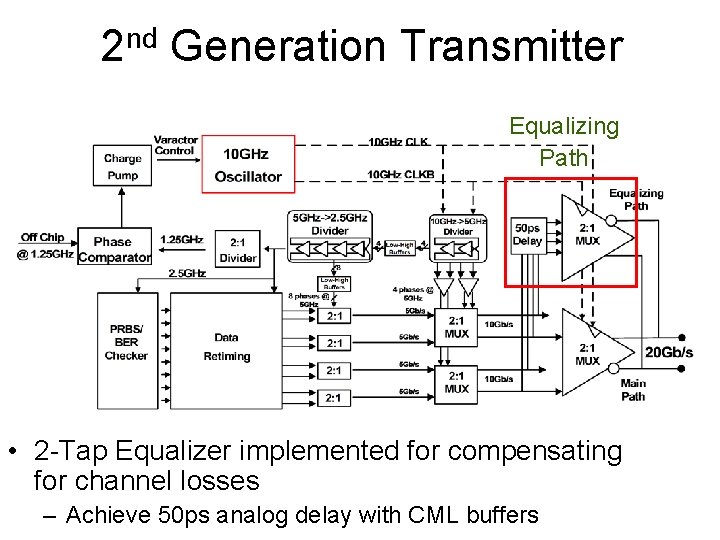
2 nd Generation Transmitter Equalizing Path • 2 -Tap Equalizer implemented for compensating for channel losses – Achieve 50 ps analog delay with CML buffers

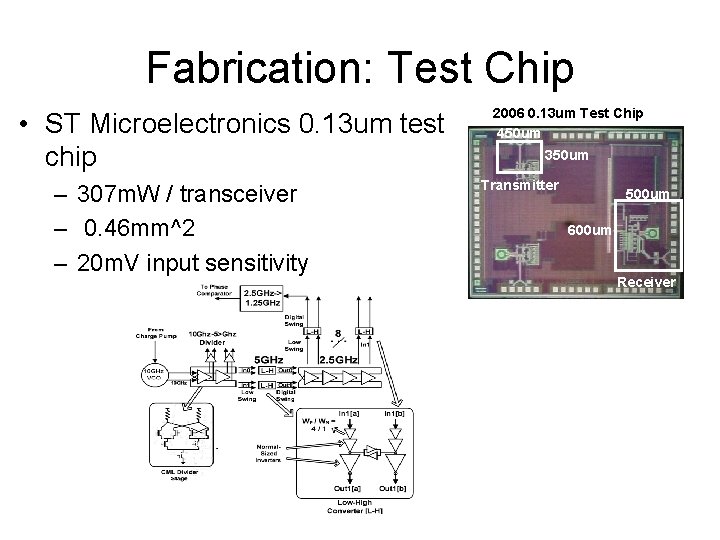
Fabrication: Test Chip • ST Microelectronics 0. 13 um test chip – 307 m. W / transceiver – 0. 46 mm^2 – 20 m. V input sensitivity 2006 0. 13 um Test Chip 450 um 350 um Transmitter 500 um 600 um Receiver

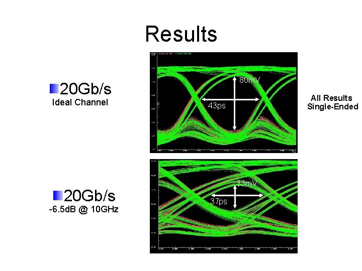
Results 80 m. V 20 Gb/s Ideal Channel 20 Gb/s -6. 5 d. B @ 10 GHz All Results Single-Ended 43 ps 33 m. V 37 ps

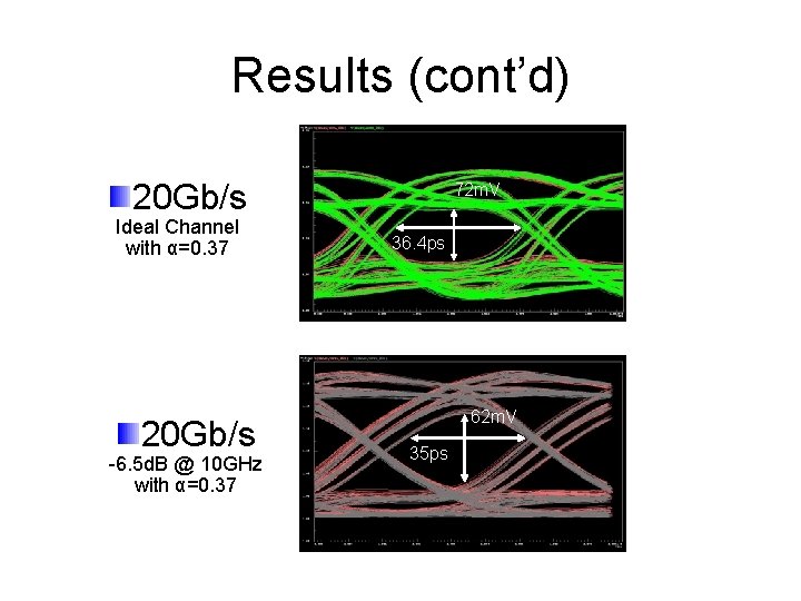
Results (cont’d) 20 Gb/s Ideal Channel with α=0. 37 20 Gb/s -6. 5 d. B @ 10 GHz with α=0. 37 72 m. V 36. 4 ps 62 m. V 35 ps

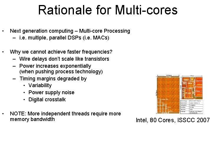
Rationale for Multi-cores • Next generation computing – Multi-core Processing – i. e. multiple, parallel DSPs (i. e. MACs) • Why we cannot achieve faster frequencies? – Wire delays don’t scale like transistors – Power increases exponentially (when pushing process technology) – Timing margins degraded by • Variability • Power supply noise • Digital crosstalk • NOTE: More independent threads require more memory bandwidth Intel, 80 Cores, ISSCC 2007

Research: Explore Parallel Serial Links also exhibit the same characteristics – Channel losses get worse – Power consumption increases significantly with bandwidth – Timing precision limited by: • Static Phase Offset (process variation) • Power-supply Induced Jitter • Interchannel Crosstalk Serial Links need to to also push for high amounts of parallelism – How is this different than conventional link design? • Channel equalization becomes more difficult – Adjacent channel crosstalk – Difficult channel estimation problem (power, flexibility, data-rate, equalizer design, channel, distance) • Amortize Clock Power for Multiple Links – Distributed resonant clocking of analog/mixed-signal front-end’s

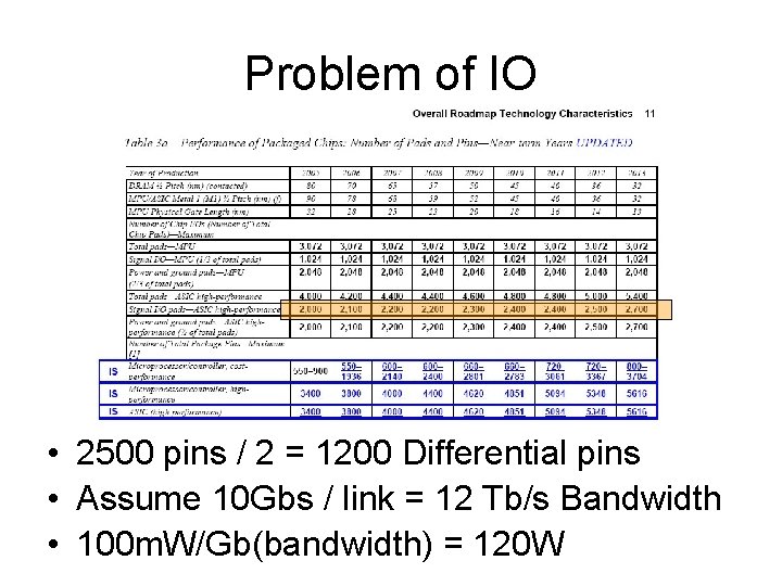
Problem of IO • 2500 pins / 2 = 1200 Differential pins • Assume 10 Gbs / link = 12 Tb/s Bandwidth • 100 m. W/Gb(bandwidth) = 120 W


Stateye Playing • Fun with Stat-Eye – 5 Gb/s -> 10 Gb/s – Worse Channels – Worse timing jitter • Homework examples

Next Time • Telegrapher’s Equation – Reflection coefficients • Channel Models – Skin Effect – Dielectric constant – vias

