ECE 667 Synthesis and Verification of Digital Circuits
![Digital Filter – Unscheduled DFG input x 1; output y 1; wire [7: 0] Digital Filter – Unscheduled DFG input x 1; output y 1; wire [7: 0]](https://slidetodoc.com/presentation_image_h/d25bf95d0374a52fbfd042682d3134cb/image-12.jpg)
- Slides: 59

ECE 667 Synthesis and Verification of Digital Circuits Introduction Design Flow 1 ECE 667 Synthesis & Verification - Design Flow

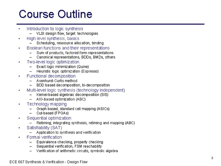
Course Outline • • • Introduction to logic synthesis – VLSI design flow, target technologies High level synthesis, basics – Scheduling, resoource allocation, binding Boolean functions and their representations – – Sum of products, factored form representations Canonical representations, BDDs, BMDs, others Two-level logic optimization – – Exact logic minimization (Quine) Heuristic logic optimization (Espresso) Functional decomposition – – Asenhurst-Curtis method BDD based decomposition, bi-decomposition Multi-level logic synthesis (technology independent) – – Kernel-based algebraic decomposition (SIS) AIG-based optimization (ABC) Technology mapping – – Graph based, standard cell mapping (ASICs) Cut-based (FPGAs) Sequential optimization – Retiming; integrating synthesis, retiming and mapping (ABC) Satisfiability (SAT) – Application to synthesis and verification Formal verification – – – Equivalence checking, property checking Sequential verification, FSM reachability Verification of arithmetic circuits, symbolic algebra 2 ECE 667 Synthesis & Verification - Design Flow

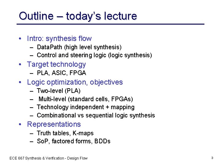
Outline – today’s lecture • Intro: synthesis flow – Data. Path (high level synthesis) – Control and steering logic (logic synthesis) • Target technology – PLA, ASIC, FPGA • Logic optimization, objectives – – Two-level (PLA) Multi-level (standard cells, FPGAs) Technology independent + mapping Combinational vs sequential logic synthesis • Representations – Truth tables, K-maps – So. P, factored forms, BDDs ECE 667 Synthesis & Verification - Design Flow 3

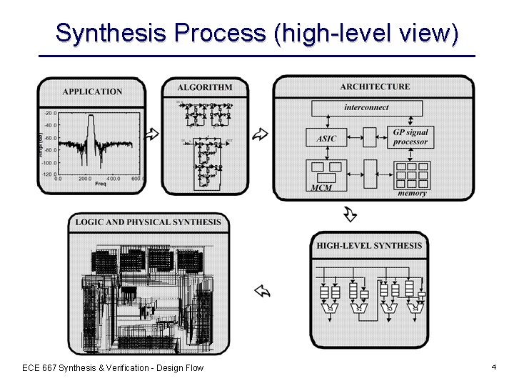
Synthesis Process (high-level view) ECE 667 Synthesis & Verification - Design Flow 4

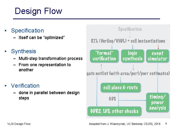
Design Flow • Specification – Itself can be “optimized” • Synthesis – Multi-step transformation process – From one representation to another • Verification – done in parallel between design steps VLSI Design Flow Adapted from J. Wawrzynek, UC Berkeley CS 250, 2016 5

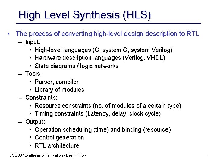
High Level Synthesis (HLS) • The process of converting high-level design description to RTL – Input: • High-level languages (C, system Verilog) • Hardware description languages (Verilog, VHDL) • State diagrams / logic networks – Tools: • Parser, compiler • Library of modules – Constraints: • Resource constraints (no. of modules of a certain type) • Timing constraints (Latency, delay, clock cycle) – Output: • Operation scheduling (time) and binding (resource) • Control generation • RTL architecture ECE 667 Synthesis & Verification - Design Flow 6

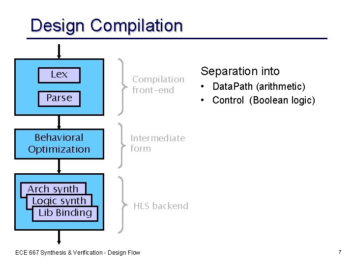
Design Compilation Lex Parse Behavioral Optimization Arch synth Logic synth Lib Binding Compilation front-end Separation into • Data. Path (arithmetic) • Control (Boolean logic) Intermediate form HLS backend ECE 667 Synthesis & Verification - Design Flow 7

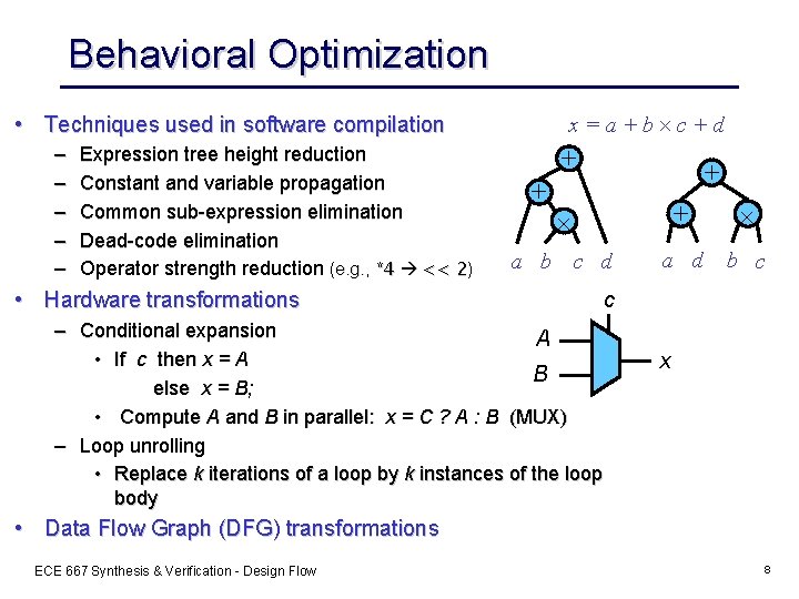
Behavioral Optimization x=a+b c+d • Techniques used in software compilation – – – Expression tree height reduction Constant and variable propagation Common sub-expression elimination Dead-code elimination Operator strength reduction (e. g. , *4 << 2) + a b + + + a d b c c d • Hardware transformations – Conditional expansion A • If c then x = A B else x = B; • Compute A and B in parallel: x = C ? A : B (MUX) – Loop unrolling • Replace k iterations of a loop by k instances of the loop body c x • Data Flow Graph (DFG) transformations ECE 667 Synthesis & Verification - Design Flow 8

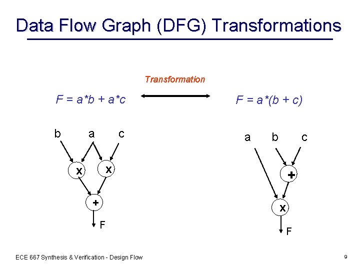
Data Flow Graph (DFG) Transformations Transformation F = a*b + a*c b a c F = a*(b + c) a b c x x + + x F ECE 667 Synthesis & Verification - Design Flow F 9

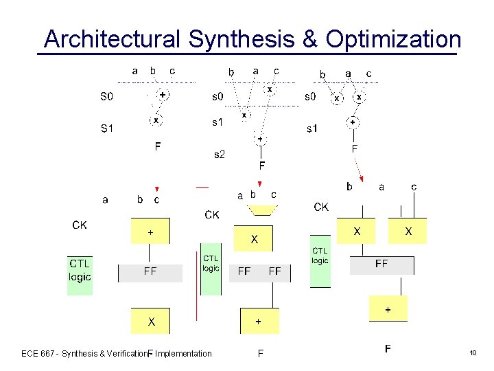
Architectural Synthesis & Optimization ECE 667 - Synthesis & Verification - Implementation 10

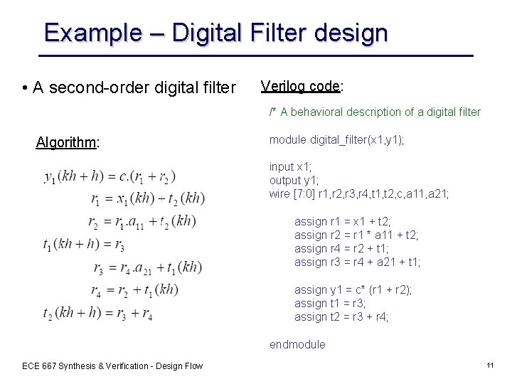
Example – Digital Filter design • A second-order digital filter Verilog code: /* A behavioral description of a digital filter Algorithm: module digital_filter(x 1, y 1); input x 1; output y 1; wire [7: 0] r 1, r 2, r 3, r 4, t 1, t 2, c, a 11, a 21; assign r 1 = x 1 + t 2; assign r 2 = r 1 * a 11 + t 2; assign r 4 = r 2 + t 1; assign r 3 = r 4 + a 21 + t 1; assign y 1 = c* (r 1 + r 2); assign t 1 = r 3; assign t 2 = r 3 + r 4; endmodule ECE 667 Synthesis & Verification - Design Flow 11
![Digital Filter Unscheduled DFG input x 1 output y 1 wire 7 0 Digital Filter – Unscheduled DFG input x 1; output y 1; wire [7: 0]](https://slidetodoc.com/presentation_image_h/d25bf95d0374a52fbfd042682d3134cb/image-12.jpg)
Digital Filter – Unscheduled DFG input x 1; output y 1; wire [7: 0] r 1, r 2, r 3, r 4, t 1, t 2, c, a 11, a 21; assign r 1 = x 1 + t 2; assign r 2 = r 1 * a 11 + t 2; assign r 4 = r 2 + t 1; assign r 3 = r 4 + a 21 + t 1; assign y 1 = c* (r 1 + r 2); assign t 1 = r 3; assign t 2 = r 3 + r 4; endmodule ECE 667 Synthesis & Verification - Design Flow 12

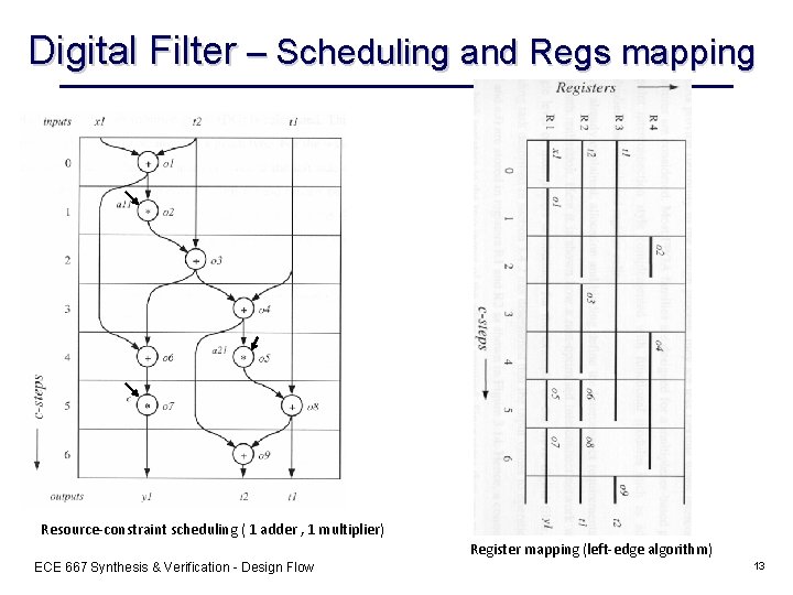
Digital Filter – Scheduling and Regs mapping Resource-constraint scheduling ( 1 adder , 1 multiplier) Register mapping (left-edge algorithm) ECE 667 Synthesis & Verification - Design Flow 13

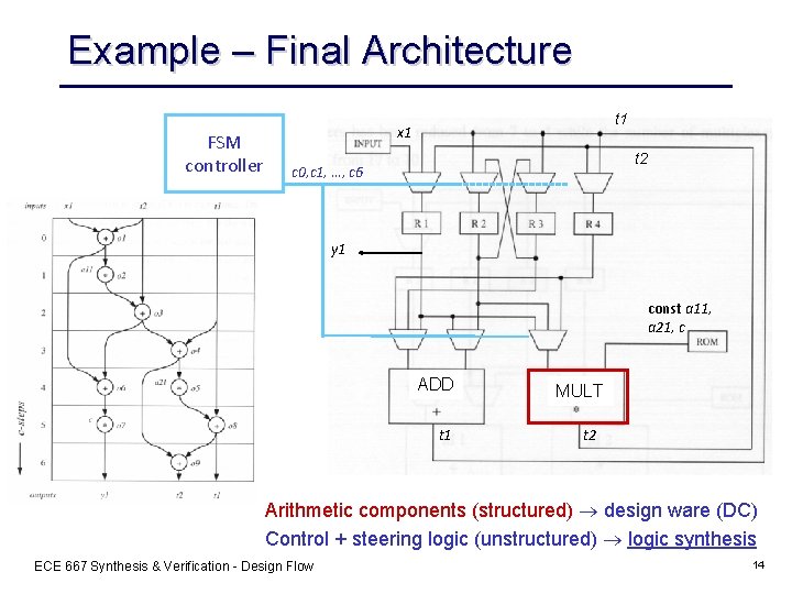
Example – Final Architecture FSM controller t 1 x 1 t 2 c 0, c 1, …, c 6 y 1 const a 11, a 21, c ADD t 1 MULT t 2 Arithmetic components (structured) design ware (DC) Control + steering logic (unstructured) logic synthesis ECE 667 Synthesis & Verification - Design Flow 14

Additional Architectural Optimization • Retiming – Changing position of synchronizing registers w/out changing overall function • On architectural level: – Goal: minimize delays (not latency) – Example: retiming of FIR filter type I into type II • Reverse the order of output • Perform retiming to minimize delay from M+n. A to M+A • Also applicable to gate-level designs VLSI Design Flow 15

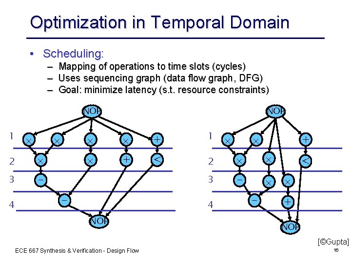
Optimization in Temporal Domain • Scheduling: – Mapping of operations to time slots (cycles) – Uses sequencing graph (data flow graph, DFG) – Goal: minimize latency (s. t. resource constraints) NOP 1 2 3 - 4 NOP + 1 + < 2 3 - - 4 NOP + - < + NOP [©Gupta] ECE 667 Synthesis & Verification - Design Flow 16

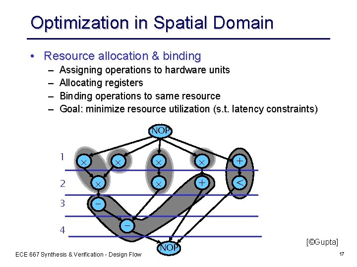
Optimization in Spatial Domain • Resource allocation & binding – – Assigning operations to hardware units Allocating registers Binding operations to same resource Goal: minimize resource utilization (s. t. latency constraints) NOP 1 2 3 - 4 + + < - ECE 667 Synthesis & Verification - Design Flow NOP [©Gupta] 17

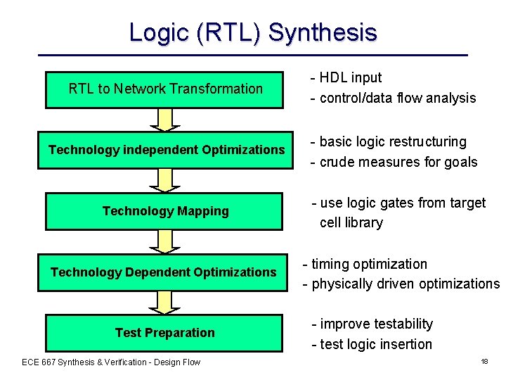
Logic (RTL) Synthesis RTL to Network Transformation - HDL input - control/data flow analysis Technology independent Optimizations - basic logic restructuring - crude measures for goals Technology Mapping - use logic gates from target cell library Technology Dependent Optimizations - timing optimization - physically driven optimizations Test Preparation ECE 667 Synthesis & Verification - Design Flow - improve testability - test logic insertion 18

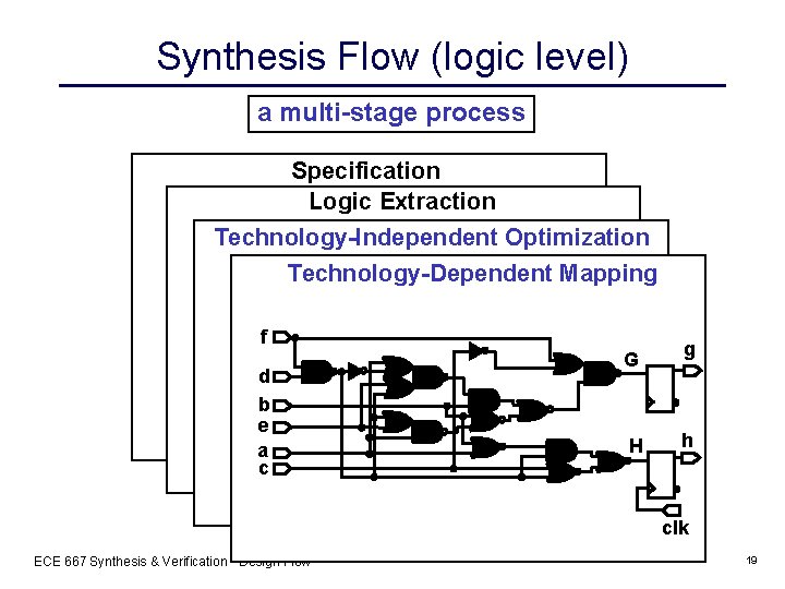
Synthesis Flow (logic level) a multi-stage process Specification Logic Extraction module example(clk, a, b, c, d, f, g, h) input clk, a, b, c, d, e, f; Technology-Independent aoutput g, h; reg g, h; Optimization b a Technology-Dependent Mapping h always @(posedge clk) begin g 1 e 0 g = a | b; G g 0 bif (d) begin if (c) h = a&~h; f g else h = b; h 5 G if (f) g = c; else a^b; dc end else g h 3 b if (c) h = 1; else h ^b; H end ed fendmodule h H h 1 ae c c clk d f clk ECE 667 Synthesis & Verification - Design Flow 19

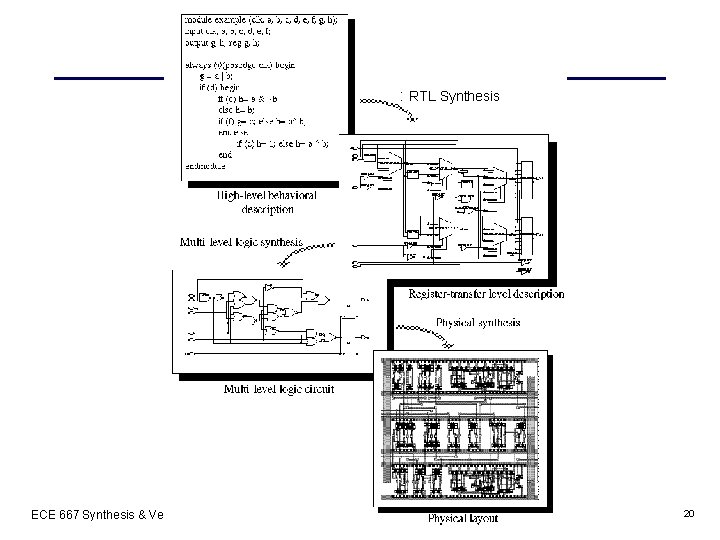
RTL Synthesis ECE 667 Synthesis & Verification - Design Flow 20

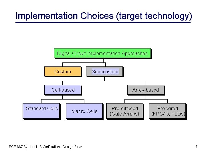
Implementation Choices (target technology) Digital Circuit Implementation Approaches Custom Semicustom Cell-based Standard Cells Macro Cells ECE 667 Synthesis & Verification - Design Flow Array-based Pre-diffused (Gate Arrays) Pre-wired (FPGAs, PLDs) 21

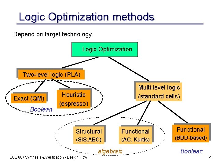
Logic Optimization methods Depend on target technology Logic Optimization Two-level logic (PLA) Exact (QM) Boolean Multi-level logic (standard cells) Heuristic (espresso) Structural Functional (SIS, ABC) (AC, Kurtis) algebraic ECE 667 Synthesis & Verification - Design Flow Functional (BDD-based) Boolean 22

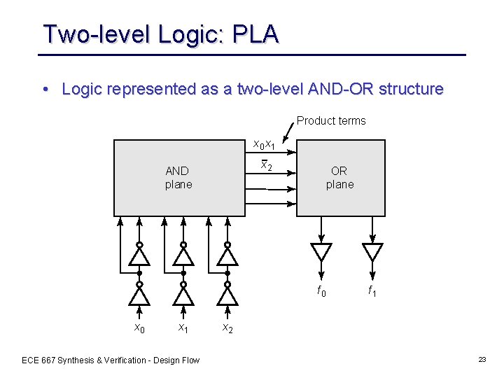
Two-level Logic: PLA • Logic represented as a two-level AND-OR structure Product terms x 0 x 1 x 2 AND plane OR plane f 0 x 1 ECE 667 Synthesis & Verification - Design Flow f 1 x 2 23

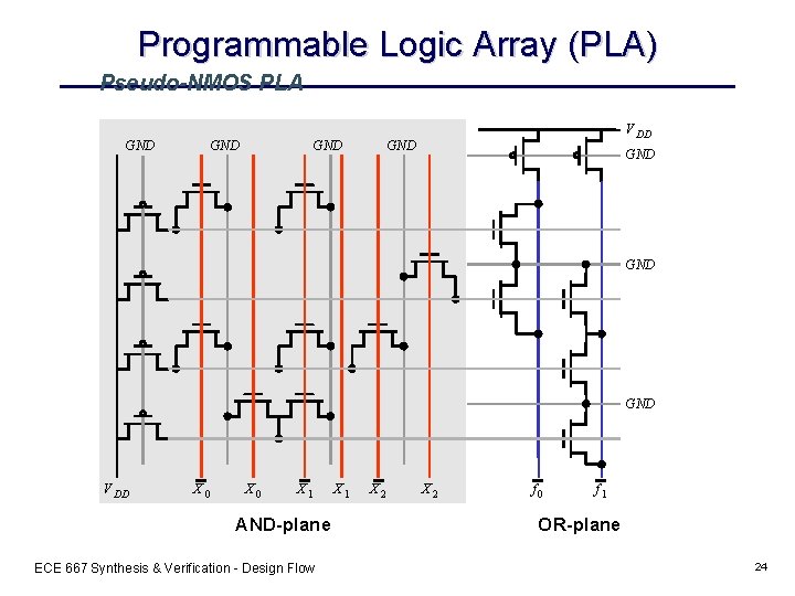
Programmable Logic Array (PLA) Pseudo-NMOS PLA GND GND V DD X 0 X 1 AND-plane ECE 667 Synthesis & Verification - Design Flow X 1 X 2 f 0 f 1 OR-plane 24

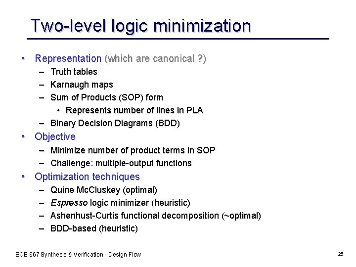
Two-level logic minimization • Representation (which are canonical ? ) – – – Truth tables Karnaugh maps Sum of Products (SOP) form • Represents number of lines in PLA – Binary Decision Diagrams (BDD) • Objective – Minimize number of product terms in SOP – Challenge: multiple-output functions • Optimization techniques – – Quine Mc. Cluskey (optimal) Espresso logic minimizer (heuristic) Ashenhust-Curtis functional decomposition (~optimal) BDD-based (heuristic) ECE 667 Synthesis & Verification - Design Flow 25

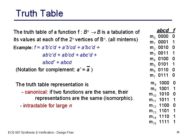
Truth Table The truth table of a function f : Bn B is a tabulation of its values at each of the 2 n vertices of Bn. (all mintems) Example: f = a’b’c’d + a’b’cd + a’bc’d + ab’cd + abc’d + abcd’ + abcd (Notation for complement: a’ = a ) The truth table representation is - canonical: if two functions are the same, their representations are the same (isomorphic). - intractable for large n ECE 667 Synthesis & Verification - Design Flow abcd f m 0 m 1 m 2 m 3 m 4 m 5 m 6 m 7 0000 0001 0010 0011 0100 0101 0110 0111 0 1 0 0 m 8 m 9 m 10 m 11 m 12 m 13 m 14 m 15 1000 1001 1010 1011 1100 1101 1110 1111 0 1 0 1 1 1 26

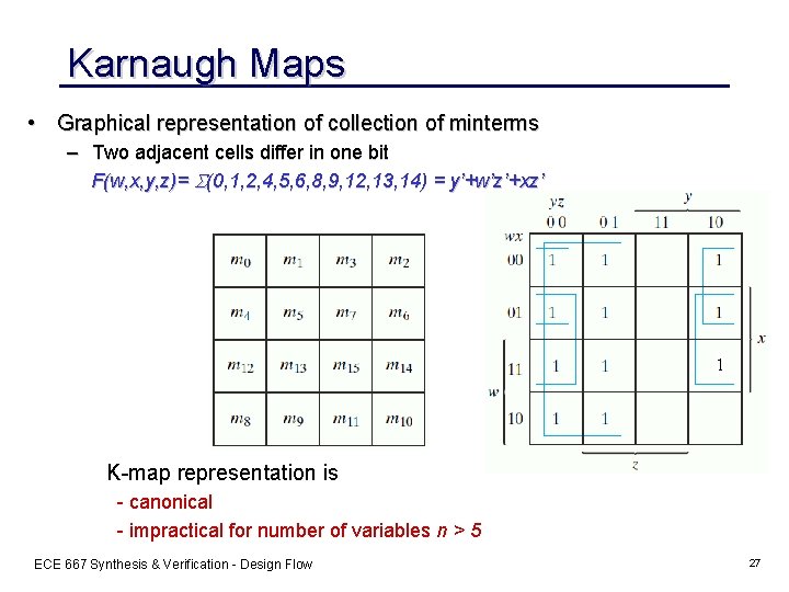
Karnaugh Maps • Graphical representation of collection of minterms – Two adjacent cells differ in one bit F(w, x, y, z)= (0, 1, 2, 4, 5, 6, 8, 9, 12, 13, 14) = y’+w’z’+xz’ 1 K-map representation is - canonical - impractical for number of variables n > 5 ECE 667 Synthesis & Verification - Design Flow 27

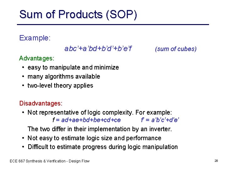
Sum of Products (SOP) Example: abc’+a’bd+b’d’+b’e’f (sum of cubes) Advantages: • easy to manipulate and minimize • many algorithms available • two-level theory applies Disadvantages: • Not representative of logic complexity. For example: f = ad+ae+bd+be+cd+ce f’ = a’b’c’+d’e’ The two differ in their implementation by an inverter. • Not easy to estimate logic size and performance • Difficult to estimate progress during logic manipulation ECE 667 Synthesis & Verification - Design Flow 28

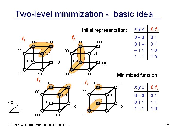
Two-level minimization - basic idea Initial representation: f 1 011 111 001 100 101 000 011 111 001 z 111 010 110 f 1 011 001 101 010 000 f 2 100 f 2 010 y 011 101 110 000 100 ECE 667 Synthesis & Verification - Design Flow 0– 0 01 01– – 11 1– 1 01 10 10 Minimized function: 010 x f 1 f 2 110 001 101 xyz 110 000 xyz f 1 f 2 0– 0 01 011 1– 1 11 10 100 29

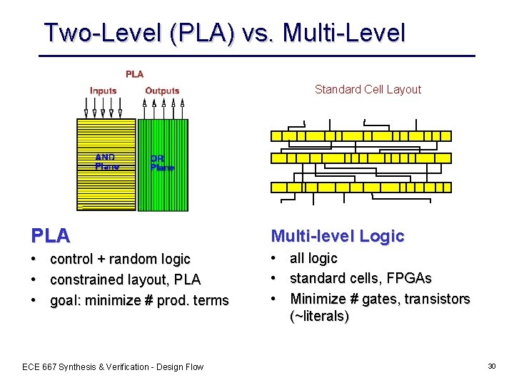
Two-Level (PLA) vs. Multi-Level Standard Cell Layout PLA Multi-level Logic • • all logic • standard cells, FPGAs • Minimize # gates, transistors (~literals) control + random logic constrained layout, PLA goal: minimize # prod. terms ECE 667 Synthesis & Verification - Design Flow 30

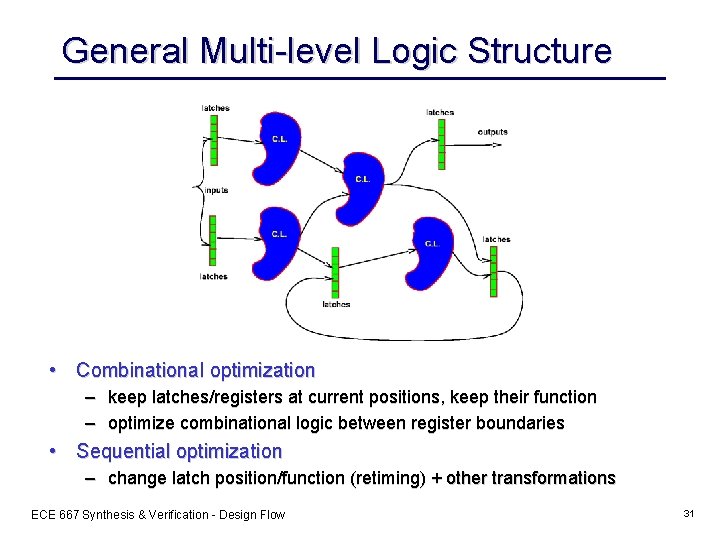
General Multi-level Logic Structure • Combinational optimization – keep latches/registers at current positions, keep their function – optimize combinational logic between register boundaries • Sequential optimization – change latch position/function (retiming) + other transformations ECE 667 Synthesis & Verification - Design Flow 31

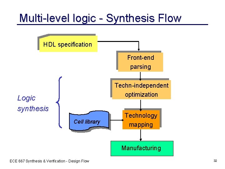
Multi-level logic - Synthesis Flow HDL specification Front-end parsing Techn-independent optimization Logic synthesis Cell library Technology mapping Manufacturing ECE 667 Synthesis & Verification - Design Flow 32

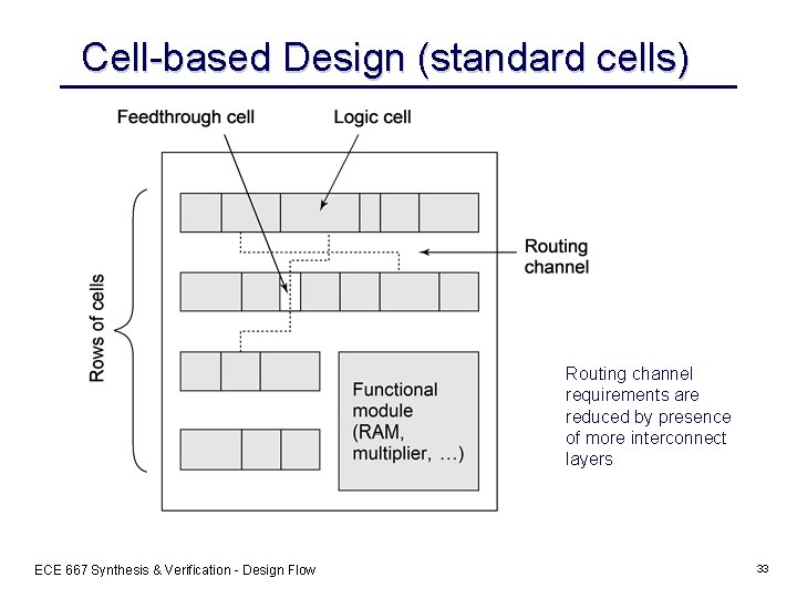
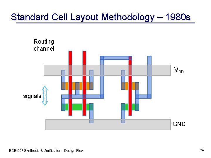
Cell-based Design (standard cells) Routing channel requirements are reduced by presence of more interconnect layers ECE 667 Synthesis & Verification - Design Flow 33

Standard Cell Layout Methodology – 1980 s Routing channel VDD signals GND ECE 667 Synthesis & Verification - Design Flow 34

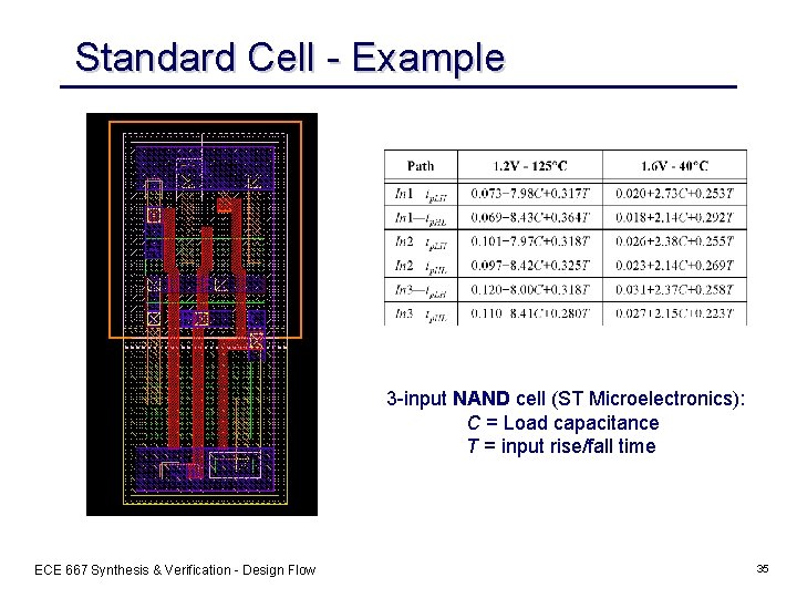
Standard Cell - Example 3 -input NAND cell (ST Microelectronics): C = Load capacitance T = input rise/fall time ECE 667 Synthesis & Verification - Design Flow 35

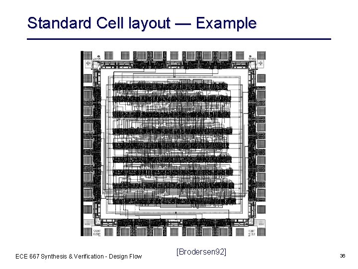
Standard Cell layout — Example ECE 667 Synthesis & Verification - Design Flow [Brodersen 92] 36

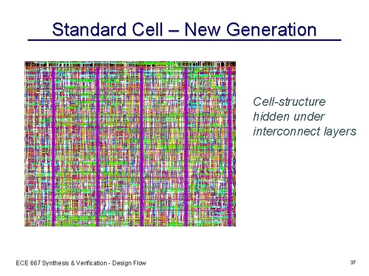
Standard Cell – New Generation Cell-structure hidden under interconnect layers ECE 667 Synthesis & Verification - Design Flow 37

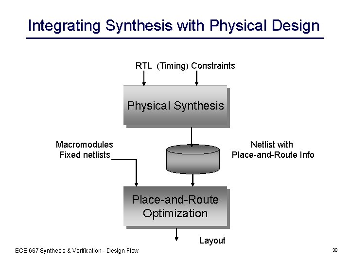
Integrating Synthesis with Physical Design RTL (Timing) Constraints Physical Synthesis Macromodules Fixed netlists Netlist with Place-and-Route Info Place-and-Route Optimization Layout ECE 667 Synthesis & Verification - Design Flow 38

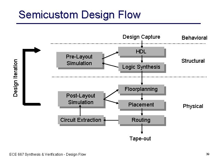
Semicustom Design Flow Design Iteration Design Capture Pre-Layout Simulation Behavioral HDL Logic Synthesis Structural Floorplanning Post-Layout Simulation Placement Circuit Extraction Routing Physical Tape-out ECE 667 Synthesis & Verification - Design Flow 39

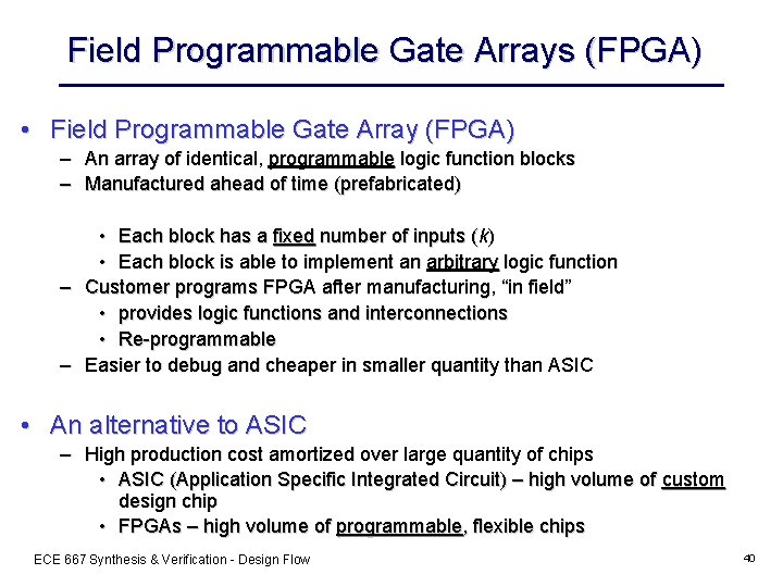
Field Programmable Gate Arrays (FPGA) • Field Programmable Gate Array (FPGA) – – An array of identical, programmable logic function blocks Manufactured ahead of time (prefabricated) • Each block has a fixed number of inputs (k) • Each block is able to implement an arbitrary logic function – Customer programs FPGA after manufacturing, “in field” • provides logic functions and interconnections • Re-programmable – Easier to debug and cheaper in smaller quantity than ASIC • An alternative to ASIC – High production cost amortized over large quantity of chips • ASIC (Application Specific Integrated Circuit) – high volume of custom design chip • FPGAs – high volume of programmable, flexible chips ECE 667 Synthesis & Verification - Design Flow 40

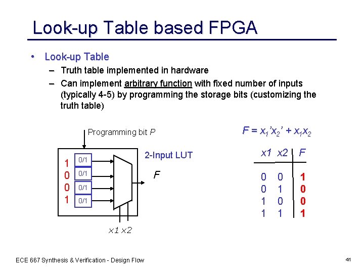
Look-up Table based FPGA • Look-up Table – Truth table implemented in hardware – Can implement arbitrary function with fixed number of inputs (typically 4 -5) by programming the storage bits (customizing the truth table) Programming bit P 1 0 0 1 2 -Input LUT 0/1 F 0/1 0/1 F = x 1’x 2’ + x 1 x 2 x 1 x 2 F 0 0 1 1 1 0 0 1 0 1 x 2 ECE 667 Synthesis & Verification - Design Flow 41

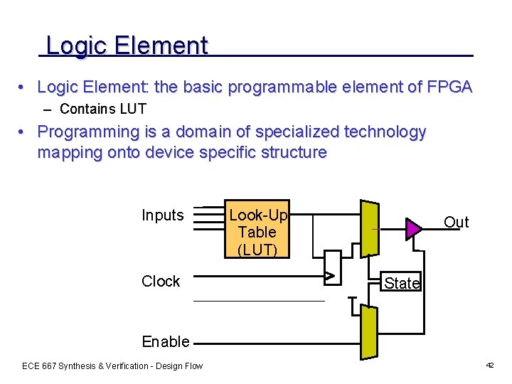
Logic Element • Logic Element: the basic programmable element of FPGA – Contains LUT • Programming is a domain of specialized technology mapping onto device specific structure Inputs Clock Look-Up Table (LUT) Out State Enable ECE 667 Synthesis & Verification - Design Flow 42

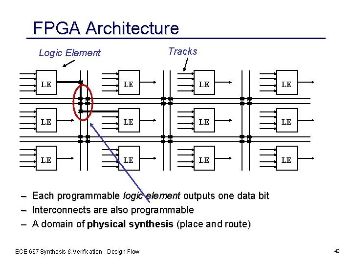
FPGA Architecture Tracks Logic Element – – – LE LE LE Each programmable logic element outputs one data bit Interconnects are also programmable A domain of physical synthesis (place and route) ECE 667 Synthesis & Verification - Design Flow 43

Multi-level logic minimization • Objective – Minimize number of literals – Literals represent inputs to CMOS gates • Representation – Factored form – Compatible with CMOS • Optimization techniques – Algebraic factorization and decomposition (heuristic) • Technology independent – Requires mapping onto target architecture • Standard cells • FPGAs (LUT) ECE 667 Synthesis & Verification - Design Flow 44

Optimization Criteria for Synthesis • Objective: minimize some function of: – Area occupied by the logic gates and interconnect (approximated by literals = transistors in technology independent optimization) – Critical path delay of the longest path through logic – Degree of testability of the circuit – Power consumed by the logic gates – Placeability, Wireability ECE 667 Synthesis & Verification - Design Flow 45

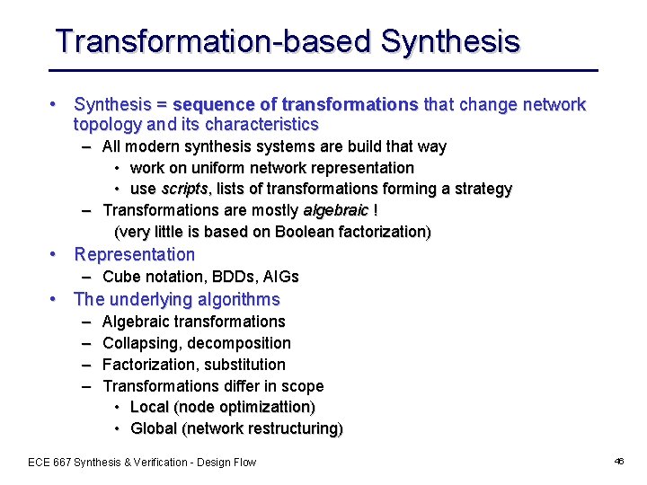
Transformation-based Synthesis • Synthesis = sequence of transformations that change network topology and its characteristics – All modern synthesis systems are build that way • work on uniform network representation • use scripts, lists of transformations forming a strategy – Transformations are mostly algebraic ! (very little is based on Boolean factorization) • Representation – Cube notation, BDDs, AIGs • The underlying algorithms – – Algebraic transformations Collapsing, decomposition Factorization, substitution Transformations differ in scope • Local (node optimizattion) • Global (network restructuring) ECE 667 Synthesis & Verification - Design Flow 46

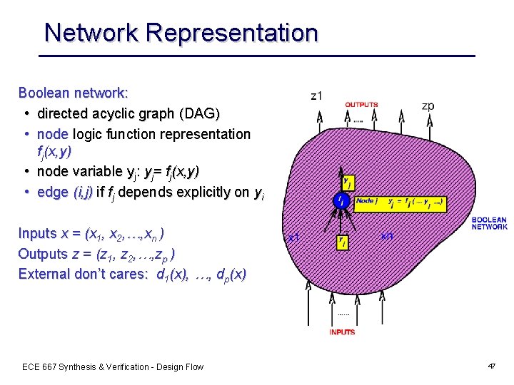
Network Representation Boolean network: • directed acyclic graph (DAG) • node logic function representation fj(x, y) • node variable yj: yj= fj(x, y) • edge (i, j) if fj depends explicitly on yi Inputs x = (x 1, x 2, …, xn ) Outputs z = (z 1, z 2, …, zp ) External don’t cares: d 1(x), …, dp(x) ECE 667 Synthesis & Verification - Design Flow 47

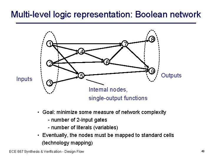
Multi-level logic representation: Boolean network 7 1 8 4 6 2 Inputs 9 5 3 Outputs Internal nodes, single-output functions • Goal: minimize some measure of network complexity - number of 2 -input gates - number of literals (variables) • Eventually, the nodes must be mapped to standard cells (technology mapping) ECE 667 Synthesis & Verification - Design Flow 48

Sum of Products (SOP) Used to represent local Boolean functions (nodes) abc’+a’bd+b’d’+b’e’f (sum of cubes) Advantages: • easy to manipulate and minimize • many algorithms available (e. g. AND, OR, TAUTOLOGY) Disadvantages: • Not representative of logic complexity. For example: f = ad+ae+bd+be+cd+ce f’ = a’b’c’+d’e’ These differ in their implementation by an inverter. • Not easy to estimate logic size and performance ECE 667 Synthesis & Verification - Design Flow 49

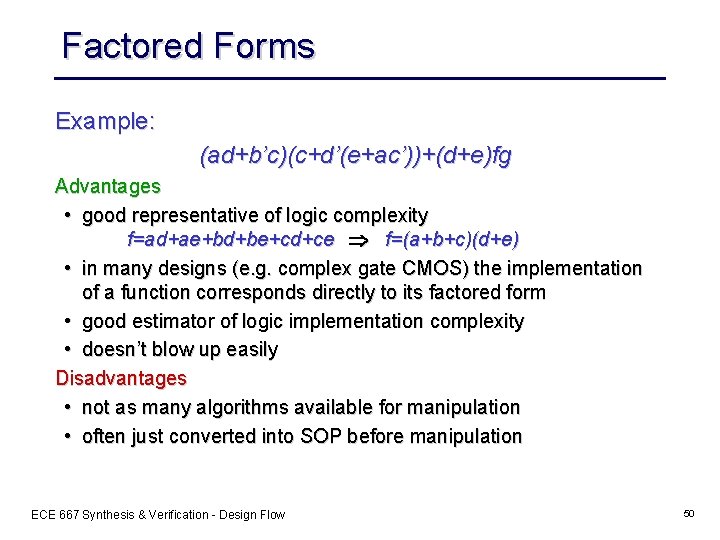
Factored Forms Example: (ad+b’c)(c+d’(e+ac’))+(d+e)fg Advantages • good representative of logic complexity f=ad+ae+bd+be+cd+ce f=(a+b+c)(d+e) • in many designs (e. g. complex gate CMOS) the implementation of a function corresponds directly to its factored form • good estimator of logic implementation complexity • doesn’t blow up easily Disadvantages • not as many algorithms available for manipulation • often just converted into SOP before manipulation ECE 667 Synthesis & Verification - Design Flow 50

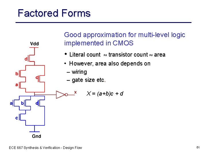
Factored Forms Good approximation for multi-level logic implemented in CMOS • Literal count » transistor count » area • However, area also depends on – wiring – gate size etc. X = (a+b)c + d ECE 667 Synthesis & Verification - Design Flow 51

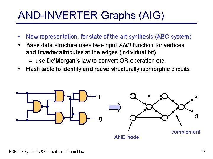
AND-INVERTER Graphs (AIG) • New representation, for state of the art synthesis (ABC system) • Base data structure uses two-input AND function for vertices and Inverter attributes at the edges (individual bit) – use De’Morgan’s law to convert OR operation etc. • Hash table to identify and reuse structurally isomorphic circuits f f g g AND node ECE 667 Synthesis & Verification - Design Flow complement 52

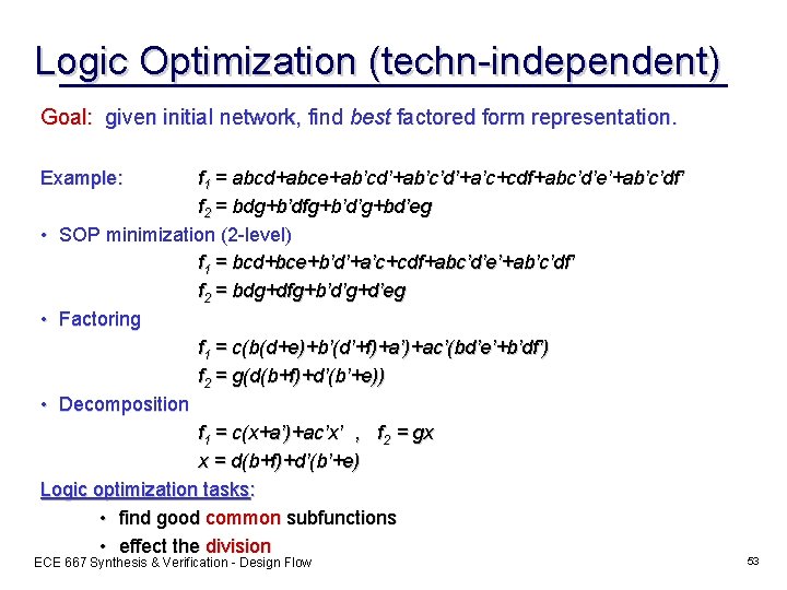
Logic Optimization (techn-independent) Goal: given initial network, find best factored form representation. Example: f 1 = abcd+abce+ab’cd’+ab’c’d’+a’c+cdf+abc’d’e’+ab’c’df’ f 2 = bdg+b’dfg+b’d’g+bd’eg • SOP minimization (2 -level) f 1 = bcd+bce+b’d’+a’c+cdf+abc’d’e’+ab’c’df’ f 2 = bdg+dfg+b’d’g+d’eg • Factoring f 1 = c(b(d+e)+b’(d’+f)+a’)+ac’(bd’e’+b’df’) f 2 = g(d(b+f)+d’(b’+e)) • Decomposition f 1 = c(x+a’)+ac’x’ , f 2 = gx x = d(b+f)+d’(b’+e) Logic optimization tasks: • find good common subfunctions • effect the division ECE 667 Synthesis & Verification - Design Flow 53

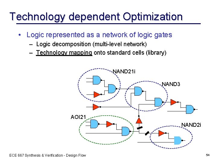
Technology dependent Optimization • Logic represented as a network of logic gates – Logic decomposition (multi-level network) – Technology mapping onto standard cells (library) NAND 21 i NAND 3 AOI 21 NAND 2 i ECE 667 Synthesis & Verification - Design Flow 54

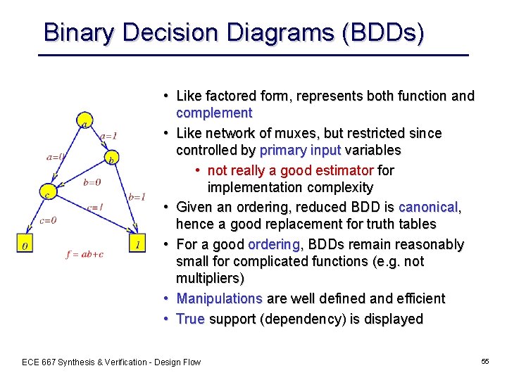
Binary Decision Diagrams (BDDs) • Like factored form, represents both function and complement • Like network of muxes, but restricted since controlled by primary input variables • not really a good estimator for implementation complexity • Given an ordering, reduced BDD is canonical, hence a good replacement for truth tables • For a good ordering, BDDs remain reasonably small for complicated functions (e. g. not multipliers) • Manipulations are well defined and efficient • True support (dependency) is displayed ECE 667 Synthesis & Verification - Design Flow 55

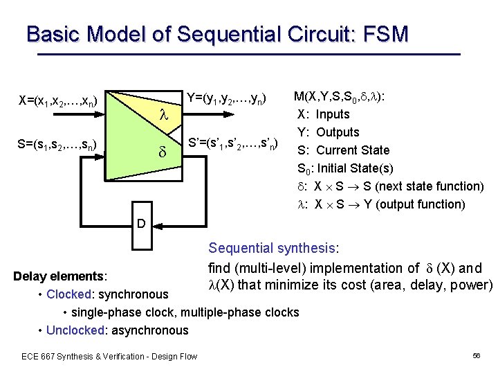
Basic Model of Sequential Circuit: FSM X=(x 1, x 2, …, xn) l S=(s 1, s 2, …, sn) d Y=(y 1, y 2, …, yn) S’=(s’ 1, s’ 2, …, s’n) M(X, Y, S, S 0, d, l): X: Inputs Y: Outputs S: Current State S 0: Initial State(s) d: X S S (next state function) l: X S Y (output function) D Sequential synthesis: find (multi-level) implementation of d (X) and l(X) that minimize its cost (area, delay, power) Delay elements: • Clocked: synchronous • single-phase clock, multiple-phase clocks • Unclocked: asynchronous ECE 667 Synthesis & Verification - Design Flow 56

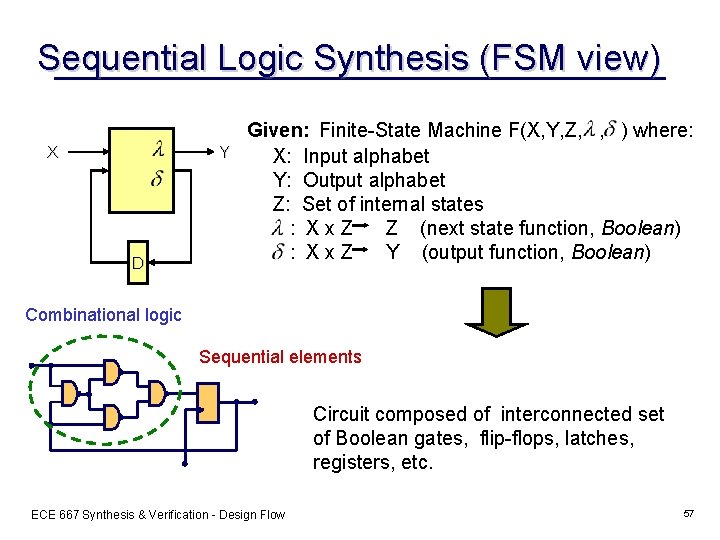
Sequential Logic Synthesis (FSM view) X Y D Given: Finite-State Machine F(X, Y, Z, , ) where: X: Input alphabet Y: Output alphabet Z: Set of internal states : Xx. Z Z (next state function, Boolean) : Xx. Z Y (output function, Boolean) Combinational logic Sequential elements Circuit composed of interconnected set of Boolean gates, flip-flops, latches, registers, etc. ECE 667 Synthesis & Verification - Design Flow 57

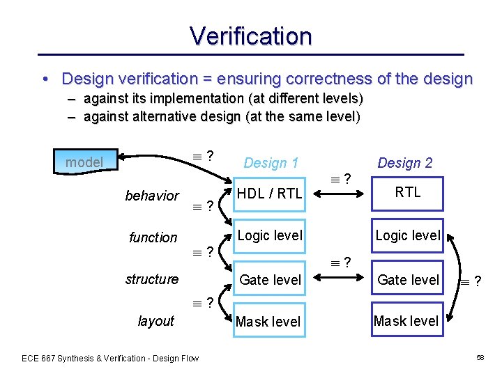
Verification • Design verification = ensuring correctness of the design – against its implementation (at different levels) – against alternative design (at the same level) ? model behavior function ? ? structure Design 1 HDL / RTL ? Logic level Design 2 RTL Logic level ? Gate level Mask level ? ? layout ECE 667 Synthesis & Verification - Design Flow 58

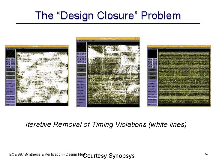
The “Design Closure” Problem Iterative Removal of Timing Violations (white lines) Courtesy Synopsys ECE 667 Synthesis & Verification - Design Flow 59