ECE 595 CMOS Analog IC Design Fall 2010




- Slides: 32

ECE 595 CMOS Analog IC Design Fall 2010 Byunghoo Jung 765 -494 -2866 jungb@purdue. edu

Instructor • Instructor: Byunghoo Jung (494 -2866, jungb@prudue. edu), Room MSEE 218 – Office hours • W 1: 00 -2: 30 PM, and F 1: 00 PM~2: 30 PM • or by appointment

Website & Text • Class Website: http: //web. ics. purdue. edu/~jungb/ECE 595 B_F 2010. h tml • Required Text: Design of Analog CMOS Integrated Circuits by Behzad Razavi (Ma. Graw-Hill) • Reference: Analysis and Design of Analog Integrated Circuits by Paul Gray, Paul Hurst, Stephen Lewis, and Robert Meyer, Fifth Edition (Wiley) • Other references: – Analog Integrated Circuit Design by David Johns and Ken Martin (Wiley) – CMOS Analog Circuit Design by Philip Allen (Oxford)

ABET Outcomes A student who successfully fulfills the course requirements will have demonstrated: • An ability to analyze bias circuit using CMOS current mirror • An ability to design differential operational amplifier • An ability to analyze basic gm-C filter • Experience in oral presentation, teamwork, and document preparation for a finished design project

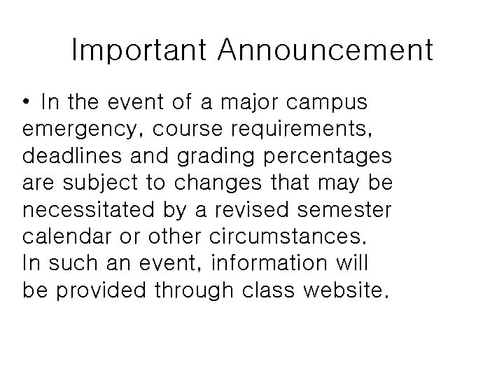
Important Announcement • In the event of a major campus emergency, course requirements, deadlines and grading percentages are subject to changes that may be necessitated by a revised semester calendar or other circumstances. In such an event, information will be provided through class website.

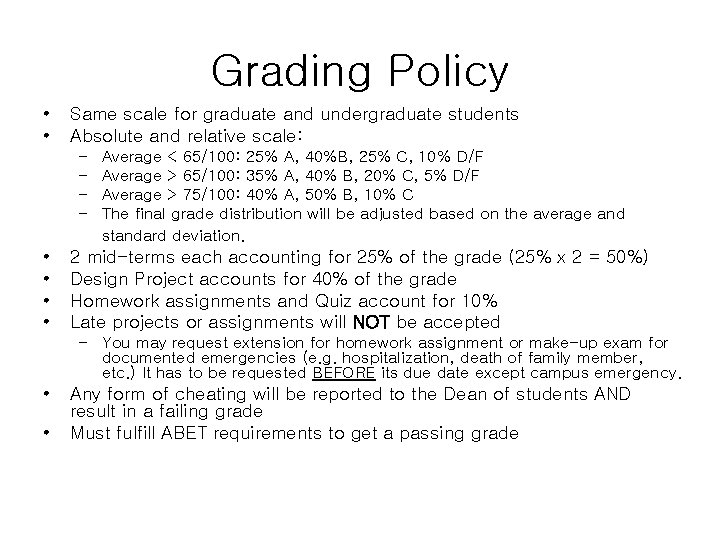
Grading Policy • • Same scale for graduate and undergraduate students Absolute and relative scale: – – • • Average < 65/100: 25% A, 40%B, 25% C, 10% D/F Average > 65/100: 35% A, 40% B, 20% C, 5% D/F Average > 75/100: 40% A, 50% B, 10% C The final grade distribution will be adjusted based on the average and standard deviation. 2 mid-terms each accounting for 25% of the grade (25% x 2 = 50%) Design Project accounts for 40% of the grade Homework assignments and Quiz account for 10% Late projects or assignments will NOT be accepted – You may request extension for homework assignment or make-up exam for documented emergencies (e. g. hospitalization, death of family member, etc. ) It has to be requested BEFORE its due date except campus emergency. • • Any form of cheating will be reported to the Dean of students AND result in a failing grade Must fulfill ABET requirements to get a passing grade

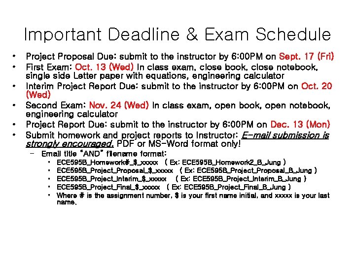
Important Deadline & Exam Schedule • • • Project Proposal Due: submit to the instructor by 6: 00 PM on Sept. 17 (Fri) First Exam: Oct. 13 (Wed) In class exam, close book, close notebook, single side Letter paper with equations, engineering calculator Interim Project Report Due: submit to the instructor by 6: 00 PM on Oct. 20 (Wed) Second Exam: Nov. 24 (Wed) In class exam, open book, open notebook, engineering calculator Project Report Due: submit to the instructor by 6: 00 PM on Dec. 13 (Mon) Submit homework and project reports to Instructor: E-mail submission is strongly encouraged. PDF or MS-Word format only! – Email title “AND” filename format: • • • ECE 595 B_Homework#_$_xxxxx ( Ex: ECE 595 B_Homework 2_B_Jung ) ECE 595 B_Project_Proposal_$_xxxxx ( Ex: ECE 595 B_Project_Proposal_B_Jung ) ECE 595 B_Project_Interim_$_xxxxx ( Ex: ECE 595 B_Project_Interim_B_Jung ) ECE 595 B_Project_Final_$_xxxxx ( Ex: ECE 595 B_Project_Final_B_Jung ) Where # is the assignment number, $ is your first name initial, and xxxxx is your last name.

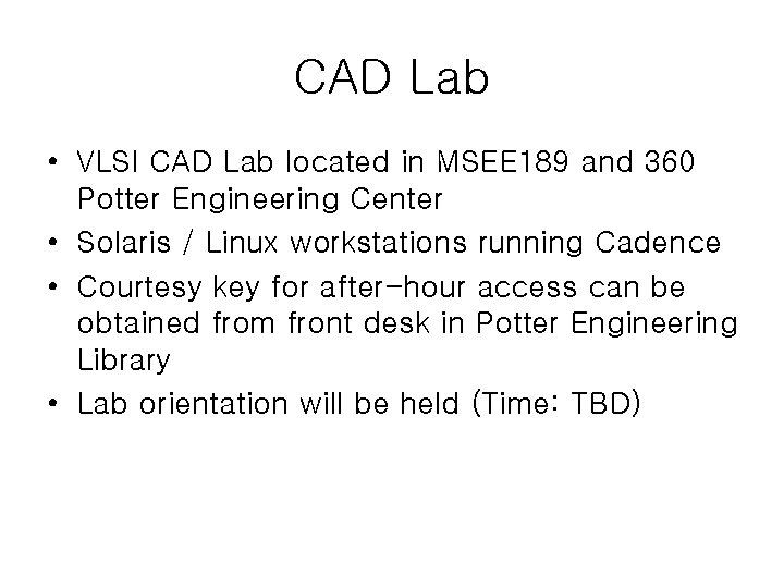
CAD Lab • VLSI CAD Lab located in MSEE 189 and 360 Potter Engineering Center • Solaris / Linux workstations running Cadence • Courtesy key for after-hour access can be obtained from front desk in Potter Engineering Library • Lab orientation will be held (Time: TBD)

Collaborations & Academic Honesty Policy • Limited collaboration among students on the design project and homework problems is encouraged – Verbal discussion of problems – Use of scratch paper or writing boards to discuss concepts and approaches to solving specific problems – OK to verbally compare the final answers obtained for a given problem as a method of checking their work – However, if you collaborate with others, please list the names of all those with whom you collaborated at the top of each solution set you hand in

Academic Honesty • The following academic honesty rules should be considered in force at all times: – Never show any draft of a homework solution to another student in the class until after the homework due date and time – Never look at any draft of another person's homework solution until after the homework due date and time – Never use another person's simulation files or supply your simulation files to another person for design project and homework – If violated, the student will receive a failing grade and the incident will be reported to the dean of the student for further administrative action

Course Outlines: 16 weeks 1. 2. 3. 4. 5. 6. 7. 8. 9. 10. 11. 12. 13. 14. 15. 16. Device physics, modeling, and layout Biasing Single stage amplifier Differential amplifier Frequency analysis. 1 st Exam Frequency analysis Noise analysis Feedback Operational amplifier. 2 nd Exam Integrated filter design

Course Outlines (Cont. ) • Many equations • Instructor will focus on the physical meanings and concepts behind the equations • Students are expected to derive the equations

Design Project • • Project Proposal Due: 6: 00 PM, Sept. 17 (Fri) Interim Project Report Due: 6: 00 PM, Oct. 20 (Wed) Final Project Report Due: 6: 00 PM, Dec. 13 (Mon) Submit homework and project reports to Instructor: E-mail submission is strongly encouraged. PDF or MS-Word format only! – Email title “AND” filename format: • • • ECE 595 B_Homework#_$_xxxxx ( Ex: ECE 595 B_Homework 2_B_Jung ) ECE 595 B_Project_Proposal_$_xxxxx ( Ex: ECE 595 B_Project_Proposal_B_Jung ) ECE 595 B_Project_Interim_$_xxxxx ( Ex: ECE 595 B_Project_Interim_B_Jung ) ECE 595 B_Project_Final_$_xxxxx ( Ex: ECE 595 B_Project_Final_B_Jung ) Where # is the assignment number, $ is your first name initial, and xxxxx is your last name.

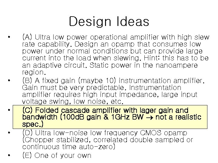
Design Ideas • • • (A) Ultra low power operational amplifier with high slew rate capability. Design an opamp that consumes low power under normal conditions but can provide large current into the load when slewing. Hint: this has to be an adaptive circuit. Static power in the nanoampere region. (B) A fixed gain (maybe 10) instrumentation amplifier. Gain must be very predictable. Instrumentation amplifier requires high input impedance, large input voltage swing, low noise, etc. (C) Folded cascade amplifier with lager gain and bandwidth (100 d. B gain & 1 GHz BW not a realistic spec. ) (D) Ultra low-noise low frequency CMOS opamp (Chopper stabilized, correlated double sampled or continuous time auto-zero) (E) One of your own

Project: Step 1 of 6 • Select project: – You are expected to work on a single project – You are advised to start thinking of topics for your final project immediately – All students have to design an op-amp as their “FIRST” project – Have to complete circuit design – Complete your op-amp design by the time the interim project report is due – You will be given more credit for innovation

Project: Still Step 1 of 6 • Select project: – The second part of your project will be to use your op-amp in a more complete design – Recommended designs are; • First order active RC filter “AND” switched capacitor filter – In the second part, you may work in group of two (optional) • If you decide to work in group of two, you have to design “second” order active RC filter AND switched capacitor filter – If you are selecting (d) or “one of your own, ” make sure that you check with me before you start – I want you to start thinking at this time and I want you to choose a general direction immediately – You can provide me with more completed details for the second part of the project during the interim project report

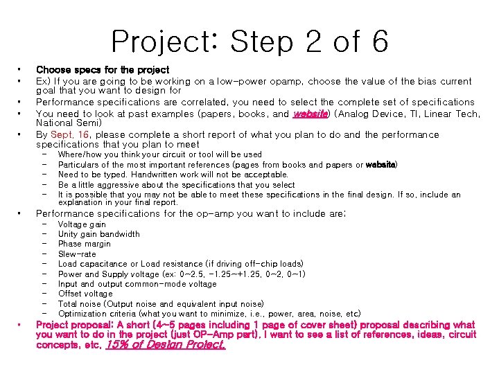
Project: Step 2 of 6 • • • Choose specs for the project Ex) If you are going to be working on a low-power opamp, choose the value of the bias current goal that you want to design for Performance specifications are correlated, you need to select the complete set of specifications You need to look at past examples (papers, books, and website) (Analog Device, TI, Linear Tech, National Semi) By Sept. 16, please complete a short report of what you plan to do and the performance specifications that you plan to meet – – – • Performance specifications for the op-amp you want to include are; – – – – – • Where/how you think your circuit or tool will be used Particulars of the most important references (pages from books and papers or website) Need to be typed. Handwritten work will not be acceptable. Be a little aggressive about the specifications that you select It is possible that you may not be able to meet these specifications in the final design. If so, include an explanation in your final report. Voltage gain Unity gain bandwidth Phase margin Slew-rate Load capacitance or Load resistance (if driving off-chip loads) Power and Supply voltage (ex: 0~2. 5, -1. 25~+1. 25, 0~2, 0~1) Input and output common-mode voltage Offset voltage Total noise (Output noise and equivalent input noise) Optimization criteria (what you want to minimize, i. e. , power, area, noise, etc) Project proposal: A short (4~5 pages including 1 page of cover sheet) proposal describing what you want to do in the project (just OP-Amp part). I want to see a list of references, ideas, circuit concepts, etc. 15% of Design Project.

Project: Step 3 of 6 • • • Complete the first part of your project Take the time to analyze your circuit Perform hand calculations and confirm using circuit simulation If questioned you need to be able to defend your choices You need to understand how the circuit works Analog circuit design cannot be learned by just taking lectures and tests. You have to DO IT to learn it. • I expect a complete design; simulations to confirm your design. • Corner simulations and Monte Carlo simulations are “NOT” required, but make sure you understand the impact of temperature / process variations, and power supply variations on your design. Don’t be a spice monkey! Enjoy the beauty of “handcraft” design!

Project: Step 4 of 6 • Write your interim project report – 10 pages (including cover page) – Needs to be neat and typed – Hand written reports will not be accepted – Even the best project if not presented well will loose its glamour – 40% of Design Project

Project: Step 5 of 6 • Complete your final project • Same as before but now you have to use your opamp in a complete system • Recommended – 1 st order active RC filter and switched capacitor filter – 2 nd order active RC filter and switched capacitor filter (if you work in group of two) – The performance will heavily depends on your op-amp design. I will check the functionality of your circuit and the completeness of your analysis (not the performance of your circuit. ) • Again “hand crafted” equations, completed design, and simulation results are required

Project: Step 6 of 6 • Write your final project report • As with the interim project report, do a good job at writing • Include everything you did on your op-amp (i. e. interim project report) in the final report • Expect length of about 20 pages (10 pages on your updated interim report + 10 pages on the complete design) • 45% of Design Project

Project: Comments • How do I design op-amps and filters before taking lectures? – When you develop a system (whether commercial or research purpose), you learn through the process. • What are the chances that you know everything about the project assigned to you? – The knowledge you can learn through class lectures is very limited (especially in analog design). – You teach “yourself” through the design process, and check what you have learned in the class.

• Questions?

• First Exam: Oct. 13 (Wed) In class exam, close book, close notebook, single side Letter paper with equations, engineering calculator • Sign on NDA • Check your login and password – Your account will be closed 7 days after the last day of the semester.

• Why analog in digital era?

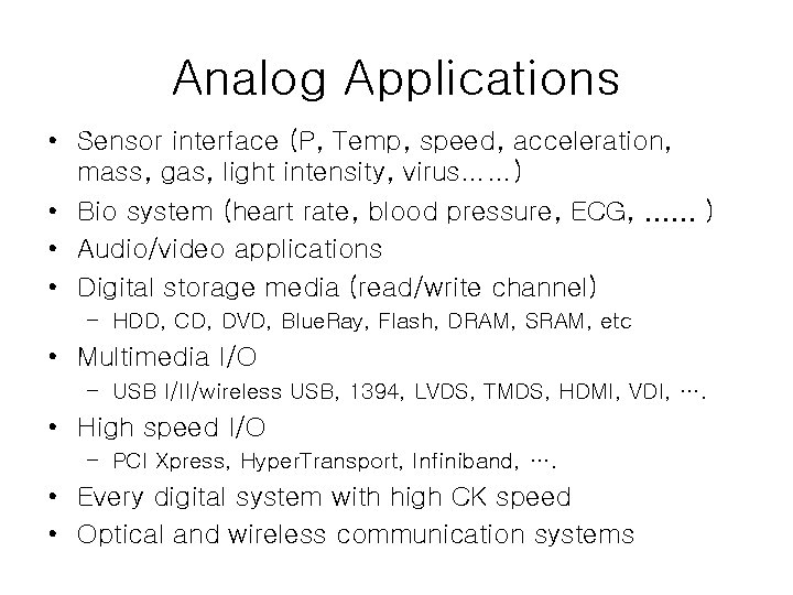
Analog Applications • Sensor interface (P, Temp, speed, acceleration, mass, gas, light intensity, virus……) • Bio system (heart rate, blood pressure, ECG, . . . ) • Audio/video applications • Digital storage media (read/write channel) – HDD, CD, DVD, Blue. Ray, Flash, DRAM, SRAM, etc • Multimedia I/O – USB I/II/wireless USB, 1394, LVDS, TMDS, HDMI, VDI, …. • High speed I/O – PCI Xpress, Hyper. Transport, Infiniband, …. • Every digital system with high CK speed • Optical and wireless communication systems

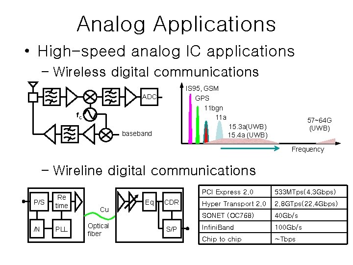
Analog Applications • High-speed analog IC applications – Wireless digital communications IS 95, GSM GPS 11 bgn 11 a ADC f. C 57~64 G (UWB) 15. 3 a(UWB) 15. 4 a (UWB) baseband Frequency – Wireline digital communications P/S /N Re time PLL Eq CDR Cu Optical fiber S/P PCI Express 2. 0 533 MTps(4. 3 Gbps) Hyper Transport 2. 0 2. 8 GTps(22. 4 Gbps) SONET (OC 768) 40 Gb/s Infini. Band 100 Gb/s Chip to chip ~Tbps

• • • Are brains analog, or digital? Hell breaks loose after Cornell claim By Andrew Orlowski in San Francisco Published Saturday 2 nd July 2005 11: 10 GMT A new study conducted at Cornell University suggests that we think in analog, not digital. It's a bold claim which, if true, threatens to make thirty years of linguistics and neuroscience metaphors look very silly indeed. • Professor Michael Spivey, a psycholinguist and associate professor of psychology at Cornell claims that the mind "should be thought of more as working the way biological organisms do: as a dynamic continuum, cascading through shades of grey. "

• It’s bad enough that hundreds of people are already “designing” CMOS VLSI without any significant knowledge of silicon devices and circuits and sometimes without much idea of the physics of hardware in the broader sense. As electronic systems become increasingly complex, this type of design will inevitably dominate, certainly for large-scale digital systems. But I wonder how many potentially useful ideas in the meadowlands of analog circuits will never be discovered because the world of the twenty -first century was taught that analog is dead? - Barrie Gilbert, “Where do little circuits come from? ” • As an old analog guru once said when comparing the analog and digital disciplines, “Any idiot can count to one, but analog design requires the engineer to make intelligent trade-offs to optimize a circuit. ” Analog design is not black or white as in “ones” and “zeros; ” analog design is shades of gray. - Samual Wilensky, “Reflections of a dinosaur”

• All the world is an analog stage and digital circuits play only bit parts. Anonymous • Analog circuit design is like chess-just because you know how the pieces move doesn’t mean you know how to play the game. Patrick M. Lahey

Quiz 1. 2. 3. Output impedance of an ideal I source? Output impedance of an ideal V source? Which element(s) generate noise? R L C Diode Transistor 4. Capacitor generates k. T/C noise. Y/N 5. It is possible to build a V or I amplifier using only passive elements. Y/N 6. Noise bandwidth is always bigger than the signal bandwidth. Y / Never heard about NBW 7. There is a system that can improve SNR, i. e. , SNR(out) > SNR(in). Y/N 8. When we mention about impedance matching, it means optimal power matching. Y/N 9. In cascaded systems, the total gain is the “multiplication” of the gains of the cascaded stages. Y/N 10. In cascaded systems, the total BW is same with the BW of the stage that has the minimum BW. Y/N 11. List names of noises that you know. Ex) thermal noise
