ECE 553 TESTING AND TESTABLE DESIGN OF DIGITAL

ECE 553: TESTING AND TESTABLE DESIGN OF DIGITAL SYSTES Test Process and Test Equipment
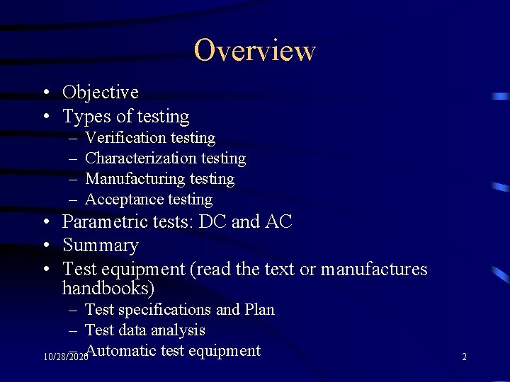
Overview • Objective • Types of testing – – Verification testing Characterization testing Manufacturing testing Acceptance testing • Parametric tests: DC and AC • Summary • Test equipment (read the text or manufactures handbooks) – Test specifications and Plan – Test data analysis – Automatic test equipment 10/28/2020 2
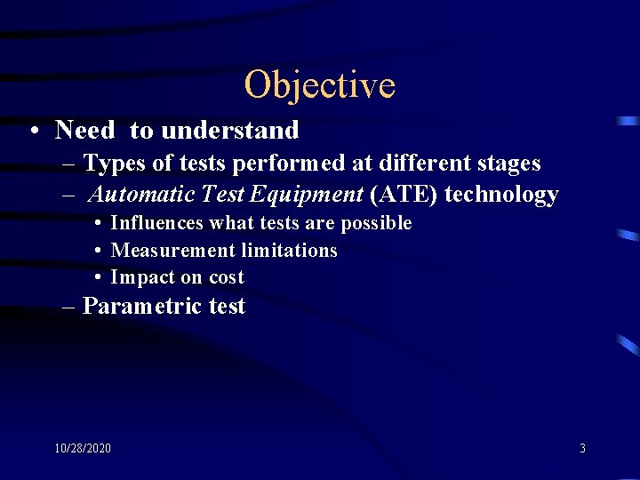
Objective • Need to understand – Types of tests performed at different stages – Automatic Test Equipment (ATE) technology • Influences what tests are possible • Measurement limitations • Impact on cost – Parametric test 10/28/2020 3
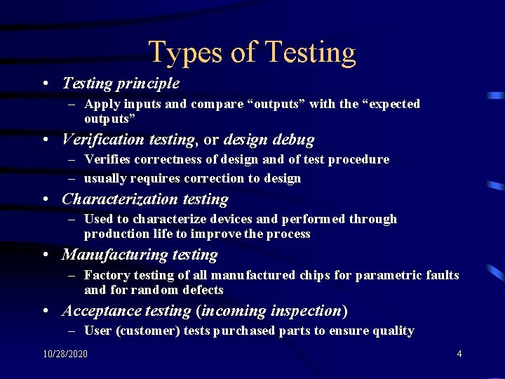
Types of Testing • Testing principle – Apply inputs and compare “outputs” with the “expected outputs” • Verification testing, or design debug – Verifies correctness of design and of test procedure – usually requires correction to design • Characterization testing – Used to characterize devices and performed through production life to improve the process • Manufacturing testing – Factory testing of all manufactured chips for parametric faults and for random defects • Acceptance testing (incoming inspection) – User (customer) tests purchased parts to ensure quality 10/28/2020 4
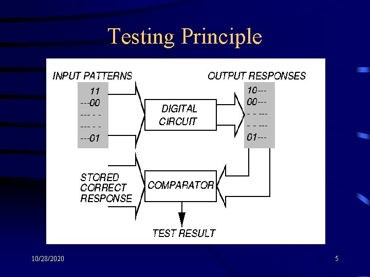
Testing Principle 10/28/2020 5
Verification Testing • Ferociously expensive • Often a software approach • But, may comprise: – – – Scanning Electron Microscope tests Bright-Lite detection of defects Electron beam testing Artificial intelligence (expert system) methods Repeated functional tests 10/28/2020 6
Characterization Test • Use of test structures – Special structures, placed on a wafer at strategic locations, are tested to characterize the process or to determine if testing of chips should proceed • Worst-case test – – – Choose test that passes/fails chips Select statistically significant sample of chips Repeat test for combination of 2+ environmental variables Plot results in Schmoo plot Diagnose and correct design errors • Continue throughout production life of chips – Improve design and process to increase yield 10/28/2020 7
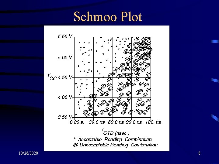
Schmoo Plot 10/28/2020 8
Manufacturing Test (Also called production test) • Determines if manufactured chip meets specs • Must cover high % of modeled faults • Must minimize test time (to control cost) • No fault diagnosis • Tests every device on chip • Test are functional or at speed of application or speed guaranteed by supplier 10/28/2020 9
Burn-in or Stress Test • Process: – Subject chips to high temperature & overvoltage supply, while running production tests • Catches: – Infant mortality cases – these are damaged chips that will fail in the first 2 days of operation – causes bad devices to actually fail before chips are shipped to customers – Freak failures – devices having same failure mechanisms as reliable devices 10/28/2020 10
Types of Manufacturing Tests • Wafer sort or probe test – done before wafer is scribed and cut into chips – Includes test site characterization – specific test devices are checked with specific patterns to measure: • Gate threshold • Polysilicon field threshold • Poly sheet resistance, etc. • Packaged device tests 10/28/2020 11
Sub-types of Tests • Parametric – measures electrical properties of pin electronics – delay, voltages, currents, etc. – fast and cheap • Functional – used to cover very high % of modeled faults – test every transistor and wire in digital circuits – long and expensive – the focus of this course 10/28/2020 12
Two Different Meanings of Functional Test • ATE and Manufacturing World – any vectors applied to cover high % of faults during manufacturing test • Automatic Test-Pattern Generation World – testing with verification vectors or vectors generated without structural information, which determine whether hardware matches its specification – typically have low fault coverage (< 70 %) 10/28/2020 13
Incoming Inspection • Can be: – Similar to production testing – More comprehensive than production testing – Tuned to specific systems application • Often done for a random sample of devices – Sample size depends on device quality and system reliability requirements – Avoids putting defective device in a system where cost of diagnosis exceeds incoming inspection cost 10/28/2020 14
Electrical Parametric Testing
Electrical Parametric Testing Typical tests DC parametric test Probe test (wafer sort) – catches gross defects Contact, power, open, short tests Functional & layout-related test AC parametric test • Unacceptable voltage/current/delay at pin • Unacceptable device operation limits 10/28/2020 16

DC Parametric Tests
Contact Test 1. Set all inputs to 0 V 2. Force current Ifb out of pin (expect Ifb to be 100 to 250 m. A) 3. Measure pin voltage Vpin. Calculate pin resistance R n Contact short (R = 0 W) n No problem n Pin open circuited (R huge), Ifb and Vpin large 10/28/2020 18
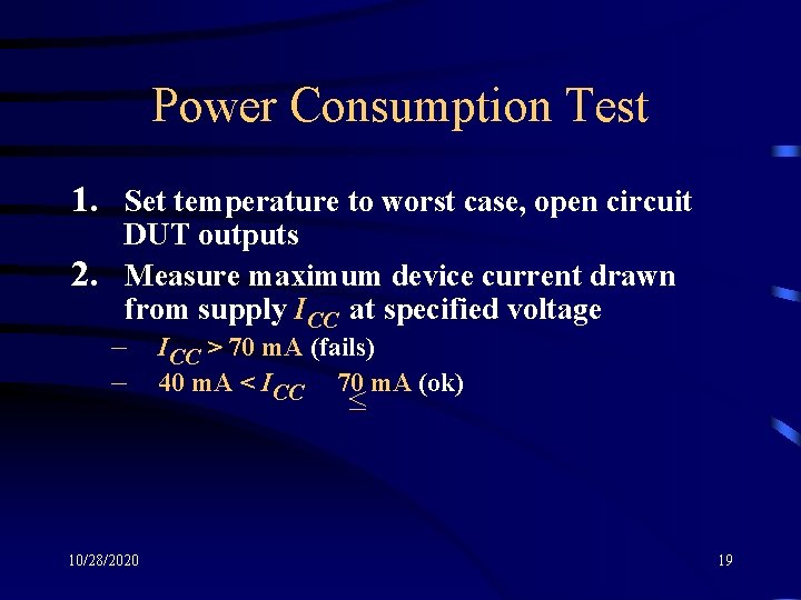
Power Consumption Test 1. Set temperature to worst case, open circuit DUT outputs 2. Measure maximum device current drawn from supply ICC at specified voltage – ICC > 70 m. A (fails) – 40 m. A < ICC 70 m. A (ok) £ 10/28/2020 19
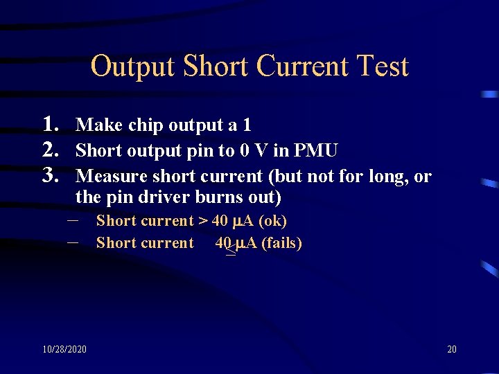
Output Short Current Test 1. Make chip output a 1 2. Short output pin to 0 V in PMU 3. Measure short current (but not for long, or the pin driver burns out) – – 10/28/2020 Short current > 40 m. A (ok) Short current 40£m. A (fails) 20
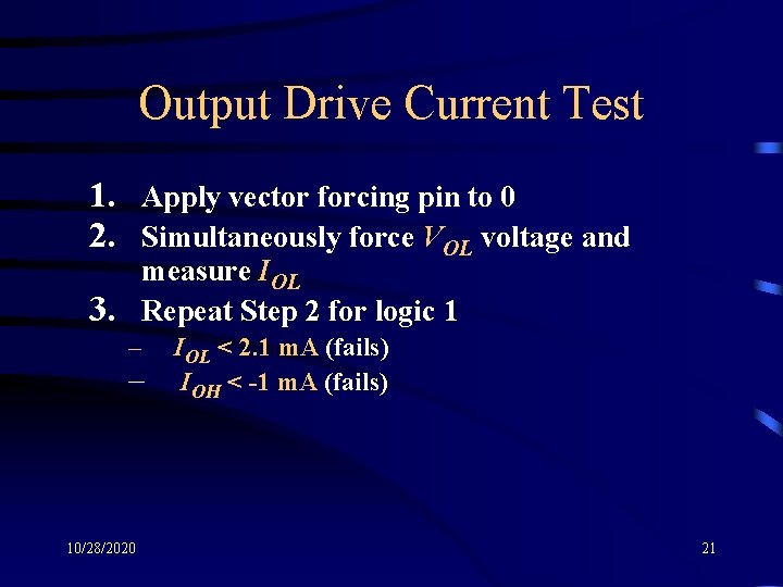
Output Drive Current Test 1. Apply vector forcing pin to 0 2. Simultaneously force VOL voltage and measure IOL 3. Repeat Step 2 for logic 1 – – 10/28/2020 IOL < 2. 1 m. A (fails) IOH < -1 m. A (fails) 21
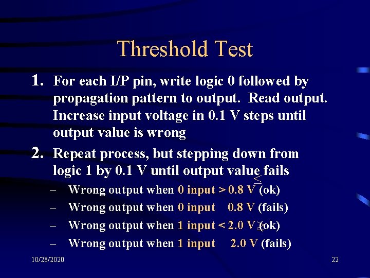
Threshold Test 1. For each I/P pin, write logic 0 followed by propagation pattern to output. Read output. Increase input voltage in 0. 1 V steps until output value is wrong 2. Repeat process, but stepping down from logic 1 by 0. 1 V until output value fails – – 10/28/2020 £ Wrong output when 0 input > 0. 8 V (ok) Wrong output when 0 input 0. 8 V (fails) Wrong output when 1 input < 2. 0 V ³ (ok) Wrong output when 1 input 2. 0 V (fails) 22

AC Parametric Tests
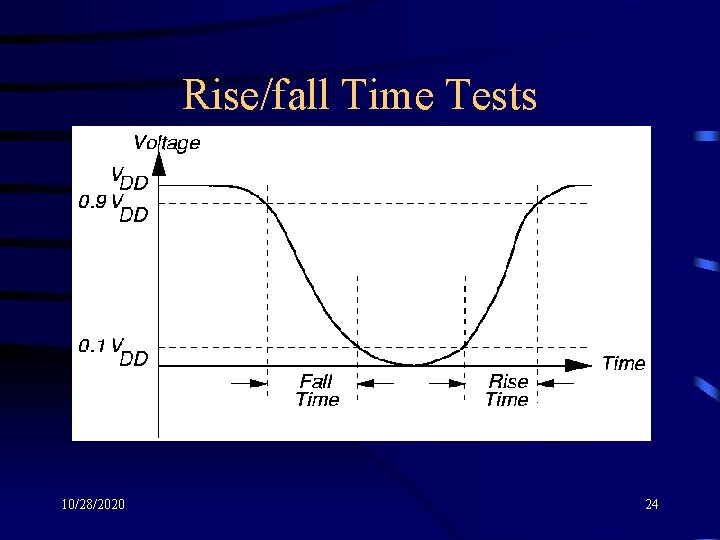
Rise/fall Time Tests 10/28/2020 24
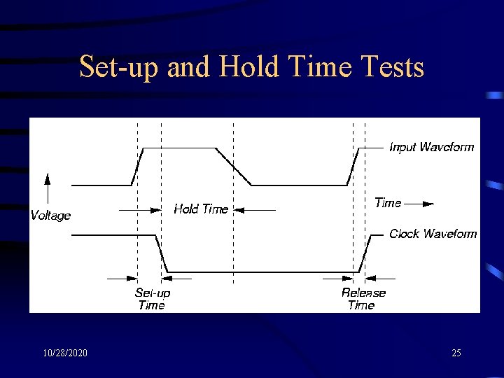
Set-up and Hold Time Tests 10/28/2020 25
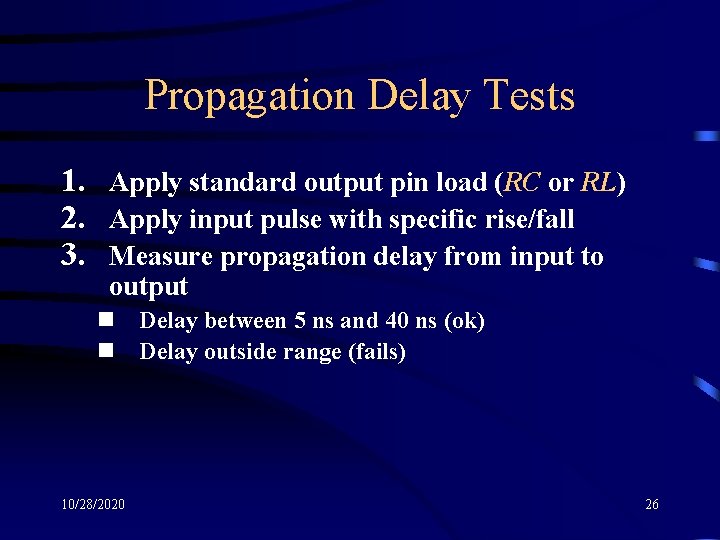
Propagation Delay Tests 1. Apply standard output pin load (RC or RL) 2. Apply input pulse with specific rise/fall 3. Measure propagation delay from input to output n Delay between 5 ns and 40 ns (ok) n Delay outside range (fails) 10/28/2020 26
Summary • Discussed many “types of testing” but alternative ways of defining types of tests exist • ATE – need to understand • Parametric testing – DC and AC • Focus of the course – structure based manufacturing testing of ICs 10/28/2020 27
Automatic Test Equipment (ATE)
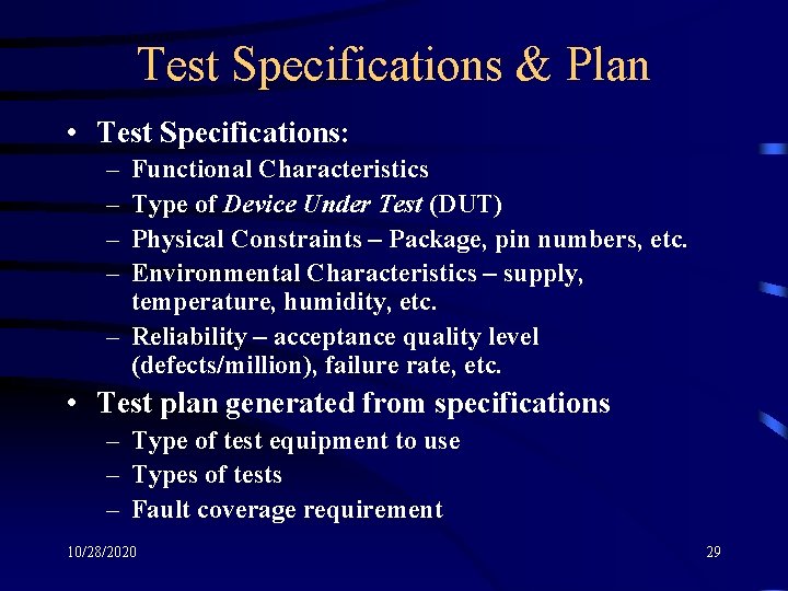
Test Specifications & Plan • Test Specifications: – – Functional Characteristics Type of Device Under Test (DUT) Physical Constraints – Package, pin numbers, etc. Environmental Characteristics – supply, temperature, humidity, etc. – Reliability – acceptance quality level (defects/million), failure rate, etc. • Test plan generated from specifications – Type of test equipment to use – Types of tests – Fault coverage requirement 10/28/2020 29
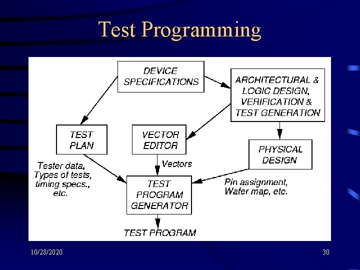
Test Programming 10/28/2020 30
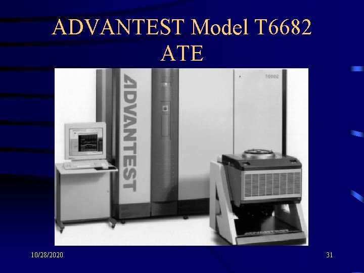
ADVANTEST Model T 6682 ATE 10/28/2020 31
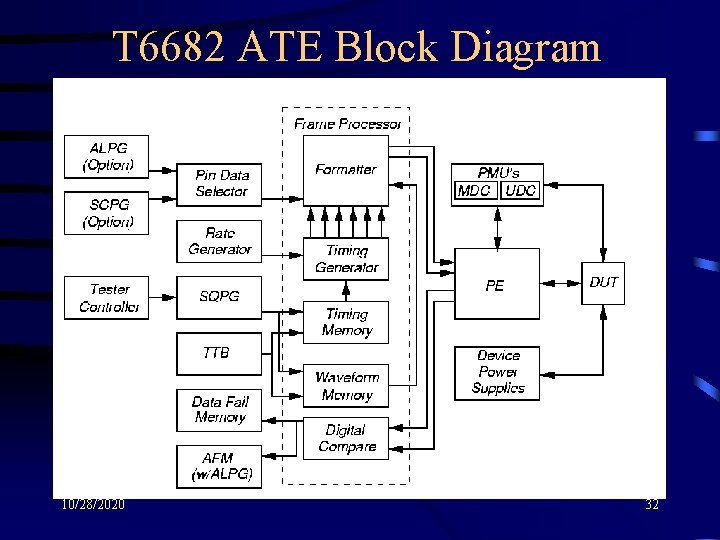
T 6682 ATE Block Diagram 10/28/2020 32
T 6682 ATE Specifications Uses 0. 35 mm VLSI chips in implementation 1024 pin channels Speed: 250, 500, or 1000 MHz Timing accuracy: +/- 200 ps Drive voltage: -2. 5 to 6 V Clock/strobe accuracy: +/- 870 ps Clock settling resolution: 31. 25 ps Pattern multiplexing: write 2 patterns in one ATE cycle • Pin multiplexing: use 2 pins to control 1 DUT pin 10/28/2020 • • 33
Pattern Generation • Sequential pattern generator (SQPG): stores 16 Mvectors of patterns to apply to DUT, vector width determined by # DUT pins • Algorithmic pattern generator (ALPG): 32 independent address bits, 36 data bits – For memory test – has address descrambler – Has address failure memory • Scan pattern generator (SCPG) supports JTAG boundary scan, greatly reduces test vector memory for full-scan testing – 2 Gvector or 8 Gvector sizes 10/28/2020 34
Response Checking and Frame Processor • Response Checking: – Pulse train matching – ATE matches patterns on 1 pin for up to 16 cycles – Pattern matching mode – matches pattern on a number of pins in 1 cycle – Determines whether DUT output is correct, changes patterns in real time • Frame Processor – combines DUT input stimulus from pattern generators with DUT output waveform comparison • Strobe time – interval after pattern application when outputs sampled 10/28/2020 35
Probing • Pin electronics (PE) – electrical buffering circuits, put as close as possible to DUT • Uses pogo pin connector at test head • Test head interface through custom printed circuit board to wafer prober (unpackaged chip test) or package handler (packaged chip test), touches chips through a socket (contactor) • Uses liquid cooling • Can independently set VIH , VIL , VOH , VOL , IH , IL , VT for each pin • Parametric Measurement Unit (PMU) 10/28/2020 36
Test Data Analysis • Uses of ATE test data: – Reject bad DUTS – Fabrication process information – Design weakness information • Devices that did not fail are good only if tests covered 100% of faults • Failure mode analysis (FMA) – Diagnose reasons for device failure, and find design and process weaknesses – Allows improvement of logic & layout design rules 10/28/2020 37
Probe Card and Probe Needles or Membrane • Probe card – custom printed circuit board (PCB) on which DUT is mounted in socket – may contain custom measurement hardware (current test) • Probe needles – come down and scratch the pads to stimulate/read pins • Membrane probe – for unpackaged wafers – contacts printed on flexible membrane, pulled down onto wafer with compressed air to get wiping action 10/28/2020 38
Multi-site Testing – Major Cost Reduction • One ATE tests several (usually identical) devices at the same time • For both probe and package test • DUT interface board has > 1 sockets • Add more instruments to ATE to handle multiple devices simultaneously • Usually test 2 or 4 DUTS at a time, usually test 32 or 64 memory chips at a time • Limits: # instruments available in ATE, type of handling equipment available for package 10/28/2020 39
- Slides: 39