ECE 551 Digital System Design Synthesis Lecture Set

- Slides: 28

ECE 551: Digital System Design & Synthesis Lecture Set 9 9. 1: Constraints and Timing 9. 2: Optimization (In separate file) 03/30/03 1

ECE 551 - Digital System Design & Synthesis Lecture 9. 1 - Constraints and Timing Overview q Constraint Concepts q Constraint Classification • • Design Rule Constraints Optimization Constraints Defining timing paths and path delays Setting Constraints 03/31/03 2

Overview (continued) q. Signal Interface Constraints • Drive characteristics for input ports • Load characteristics on output ports • Input delays and output delays 03/31/03 3

Constraint Concepts q Constraints are used to: • Define limitations required for the target technology to function properly • Specify the environment in which the design must function in terms of input drive, output loading, temperature, power supply voltage, etc. • Specify the design goals (other than functionality) in terms of bounds on input loading, output drive, area, performance, and power consumption. 03/31/03 4

References q. Design Compiler User Guide (DCUG) q. Design Compiler Reference Manual: Constraints and Timing (DCRM) q. Design Compiler Reference Manual: Optimization and Timing Analysis (DCRMO) 03/31/03 5

Classification of Constraints q. Design rule constraints • Implicit constraints defined by the technology library • Required for the design to function correctly • Apply to any design using the library q. Optimization constraints • Explicit constraints defined by the user • Represent design goals 03/31/03 6

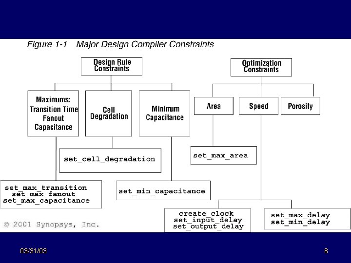
Design Constraints q Figure 1 -1 RMCT (See Next Slide) q Constraints: • • Maximum Transition Time Maximum Fanout Maximum and minimum capacitance Cell degradation q Cannot remove default values from tech lib q Can make more restrictive than tech lib values 03/31/03 7

03/31/03 8

Maximum Transition Time q. Maximum transition time for a net is the longest time required for its driving pin to change logical values. • Implies that slow transitions are to be avoided. • What’s wrong with slow transitions? q. Can be made more restrictive using set_max_transition 03/31/03 9

Maximum Fanout q Places fanout restrictions on driving pins q Each driven input or driven output port has a fanout_load value q Each driving output has a max_fanout value q Sum of driven fanout_loads must be no more than max_fanout of driver q Fanout_load is dimensionless, typically a value normalized to some unit capacitance q Can be made more restrictive by using set_max_fanout and set_fanout_load 03/31/03 10

Maximum and Minimum Capacitance q. Permits limiting capacitance directly rather than implicitly using max_fanout and max_transition q. Can make more restrictive by using set_max_capacitance q. Similar for minimum capacitance which is more of a modeling constraint and has lower priority in terms of being met. 03/31/03 11

Cell Degradation q Delays are often determined with an “ideal” input transition time on a cell q As the input transition time increases, delay increases for a given capacitive load increase q Cell degradation tables that list maximum capacitance that can be driven by a cell as a function of transition times at the inputs of a cell. q compile_fix_cell_degradation to fix table and set_cell_degradation to specify degradation. 03/31/03 12

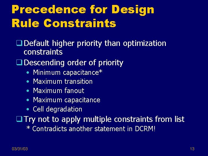
Precedence for Design Rule Constraints q Default higher priority than optimization constraints q Descending order of priority • • • Minimum capacitance* Maximum transition Maximum fanout Maximum capacitance Cell degradation q Try not to apply multiple constraints from list * Contradicts another statement in DCRM! 03/31/03 13

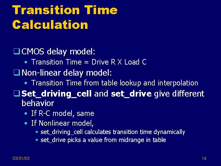
Transition Time Calculation q CMOS delay model: • Transition Time = Drive R X Load C q Non-linear delay model: • Transition Time from table lookup and interpolation q Set_driving_cell and set_drive give different behavior • If R-C model, same • If Nonlinear model, § set_driving_cell calculates transition time dynamically § set_drive picks a value from midrange in table 03/31/03 14

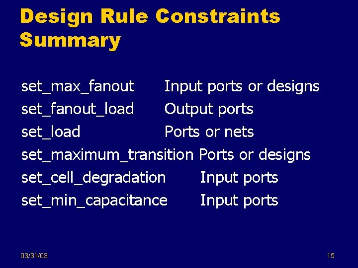
Design Rule Constraints Summary set_max_fanout Input ports or designs set_fanout_load Output ports set_load Ports or nets set_maximum_transition Ports or designs set_cell_degradation Input ports set_min_capacitance Input ports 03/31/03 15

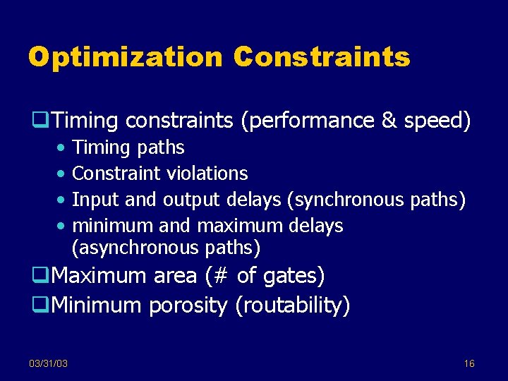
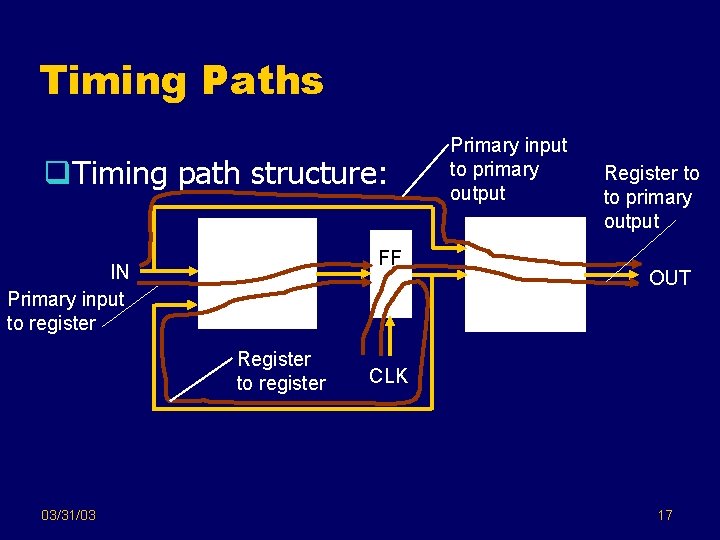
Optimization Constraints q. Timing constraints (performance & speed) • • Timing paths Constraint violations Input and output delays (synchronous paths) minimum and maximum delays (asynchronous paths) q. Maximum area (# of gates) q. Minimum porosity (routability) 03/31/03 16

Timing Paths q. Timing path structure: FF IN Primary input to register Register to register 03/31/03 Primary input to primary output Register to to primary output OUT CLK 17

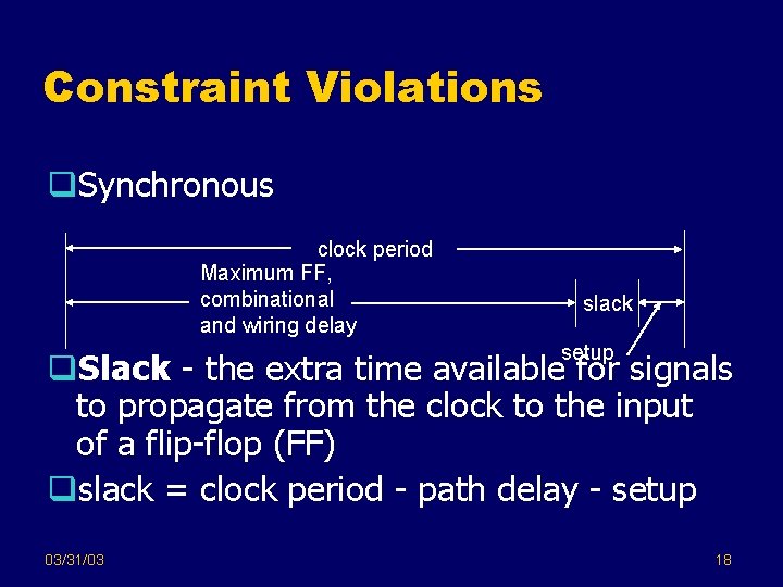
Constraint Violations q. Synchronous clock period Maximum FF, combinational and wiring delay slack setup q. Slack - the extra time available for signals to propagate from the clock to the input of a flip-flop (FF) qslack = clock period - path delay - setup 03/31/03 18

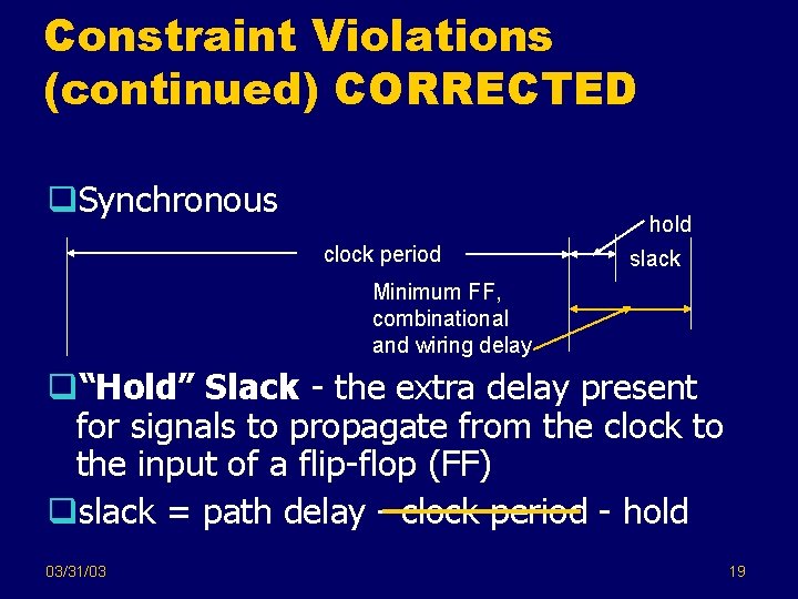
Constraint Violations (continued) CORRECTED q. Synchronous hold clock period slack Minimum FF, combinational and wiring delay q“Hold” Slack - the extra delay present for signals to propagate from the clock to the input of a flip-flop (FF) qslack = path delay - clock period - hold 03/31/03 19

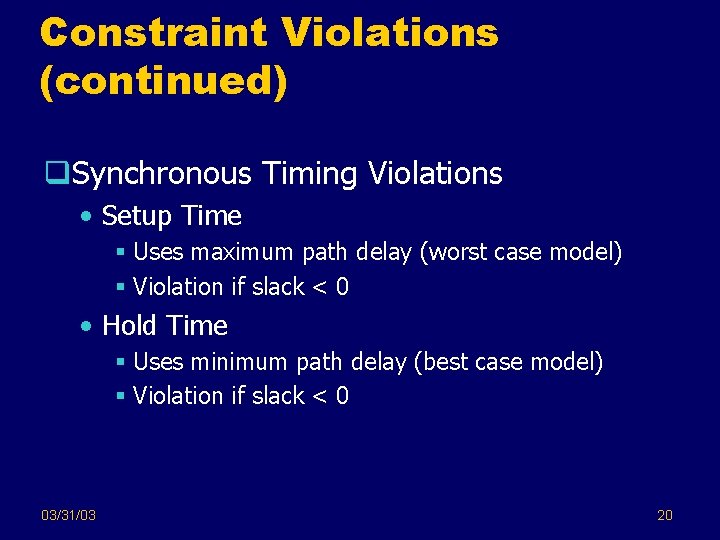
Constraint Violations (continued) q. Synchronous Timing Violations • Setup Time § Uses maximum path delay (worst case model) § Violation if slack < 0 • Hold Time § Uses minimum path delay (best case model) § Violation if slack < 0 03/31/03 20

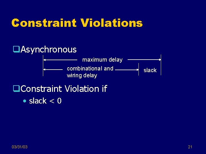
Constraint Violations q. Asynchronous maximum delay combinational and wiring delay slack q. Constraint Violation if • slack < 0 03/31/03 21

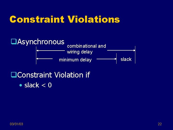
Constraint Violations q. Asynchronous combinational and wiring delay minimum delay slack q. Constraint Violation if • slack < 0 03/31/03 22

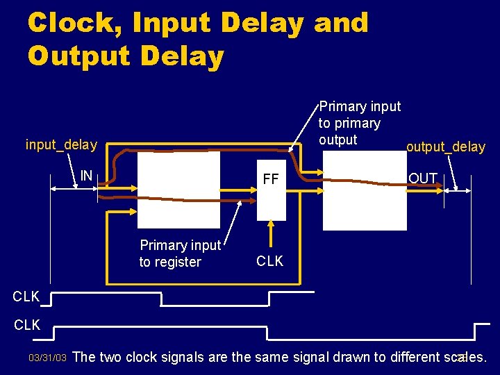
Clock, Input Delay and Output Delay Primary input to primary output_delay input_delay IN FF Primary input to register OUT CLK CLK 03/31/03 23 The two clock signals are the same signal drawn to different scales.

Clocks, Input Delay and Output Delay (continued) q Examples: • create_clock -period 3. 3 CLK § Establishes a clock CLK with period 3. 3 ns • create_clock -period 3. 3 -waveform (10, 25) -name SYS_CLK § Establishes virtual clock for system without a clock • set_input_delay 0. 3 -clock CLK IN § Value on IN is available 0. 3 ns after CLK • set_output_delay 1. 0 -clock CLK OUT § Value on OUT must be available 1. 0 ns before CLK 03/31/03 24

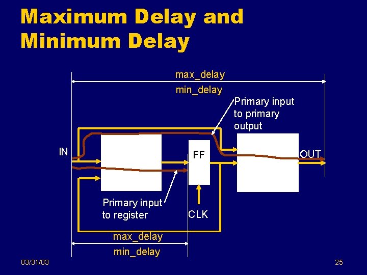
Maximum Delay and Minimum Delay max_delay min_delay Primary input to primary output IN FF Primary input to register OUT CLK max_delay min_delay 03/31/03 25

Maximum Delay and Minimum Delay (continued) q. Examples: • set_maximum_delay 2. 5 -from IN -to OUT § Specifies that the delay from IN to OUT is to be no more than 2. 5 ns • set_minimum_delay 1. 0 -from IN -to OUT § Specifies that the delay from IN to OUT is to be no less than 1. 0 ns • set_maximum_delay 1. 5 -from IN -to FF 1/D 03/31/03 26

Maximum Area qset_max_area • Specifies the maximum allowable area of the design in area units of the technology 03/31/03 27

Minimum Porosity q. Effective only for two-layer metal technology (therefore not used in our work) qset_min_porosity [design list] • Specifies the part of the total cell area to be used for over the cell routing • porosity - a percentage ratio of routing track area over cells to cell area; from 0 to 90. 03/31/03 28