ECE 546 Lecture 12 Integrated Circuits Spring 2016
- Slides: 39

ECE 546 Lecture 12 Integrated Circuits Spring 2016 Jose E. Schutt-Aine Electrical & Computer Engineering University of Illinois jesa@illinois. edu ECE 546 – Jose Schutt-Aine 1

Integrated Circuits • IC Requirements – Biasing of ICs is based on the use of constant current sources – Use current mirrors – Source circuits are used as loads ECE 546 – Jose Schutt-Aine 2

Integrated Circuits • Analog Design Requirements – Analog ICs may need resistors and capacitors for the design of amplifiers – Resistors and capacitors occupy the space of tens or hundreds of MOS devices – It is important to minimize their use ECE 546 – Jose Schutt-Aine 3

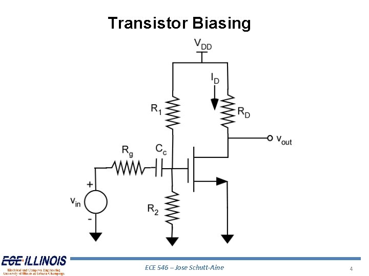
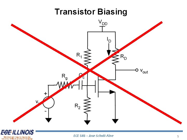
Transistor Biasing ECE 546 – Jose Schutt-Aine 4

Transistor Biasing ECE 546 – Jose Schutt-Aine 5

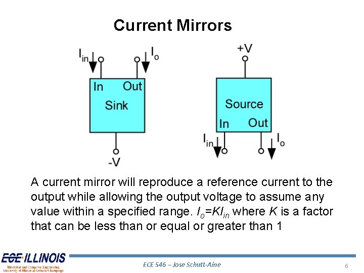
Current Mirrors A current mirror will reproduce a reference current to the output while allowing the output voltage to assume any value within a specified range. Io=KIin where K is a factor that can be less than or equal or greater than 1 ECE 546 – Jose Schutt-Aine 6

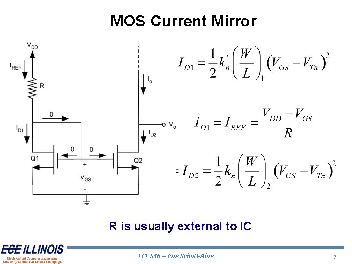
MOS Current Mirror R is usually external to IC ECE 546 – Jose Schutt-Aine 7

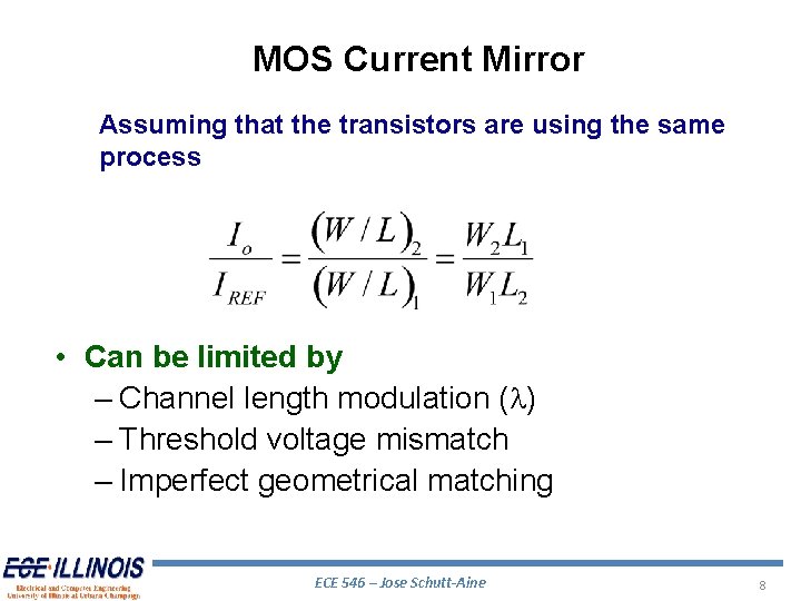
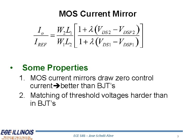
MOS Current Mirror Assuming that the transistors are using the same process • Can be limited by – Channel length modulation (l) – Threshold voltage mismatch – Imperfect geometrical matching ECE 546 – Jose Schutt-Aine 8

MOS Current Mirror • Some Properties 1. MOS current mirrors draw zero control current better than BJT’s 2. Matching of threshold voltages harder than in BJT’s ECE 546 – Jose Schutt-Aine 9

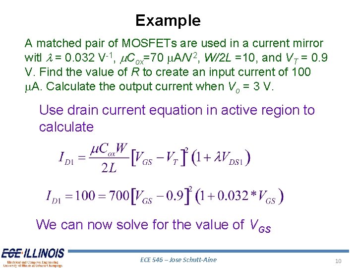
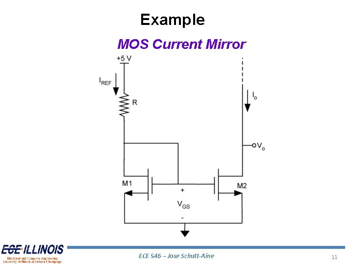
Example A matched pair of MOSFETs are used in a current mirror witl l = 0. 032 V-1, m. Cox=70 m. A/V 2, W/2 L =10, and VT = 0. 9 V. Find the value of R to create an input current of 100 m. A. Calculate the output current when Vo = 3 V. Use drain current equation in active region to calculate We can now solve for the value of VGS ECE 546 – Jose Schutt-Aine 10

Example MOS Current Mirror ECE 546 – Jose Schutt-Aine 11

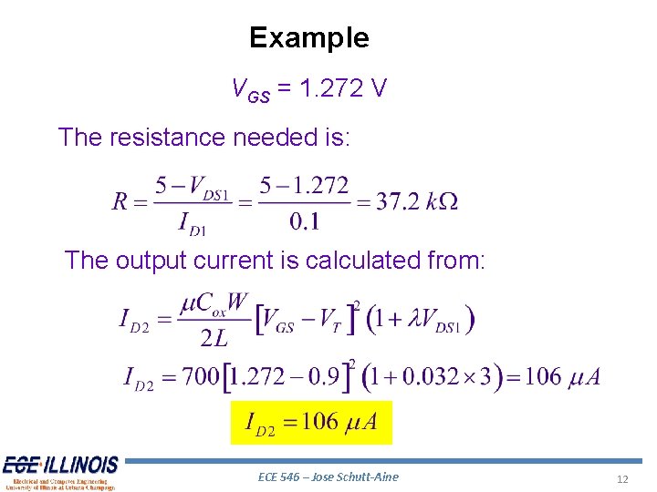
Example VGS = 1. 272 V The resistance needed is: The output current is calculated from: ECE 546 – Jose Schutt-Aine 12

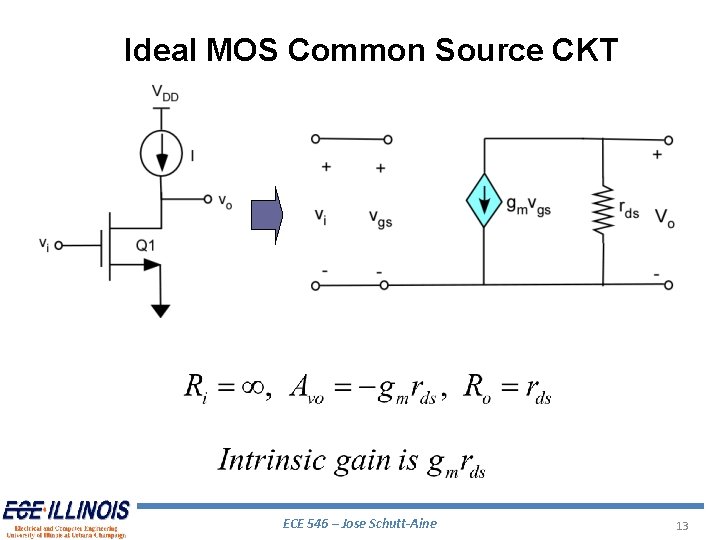
Ideal MOS Common Source CKT ECE 546 – Jose Schutt-Aine 13

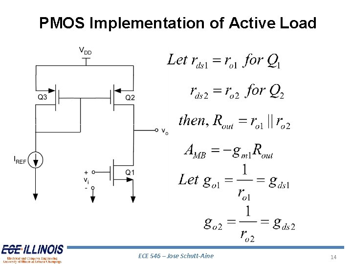
PMOS Implementation of Active Load ECE 546 – Jose Schutt-Aine 14

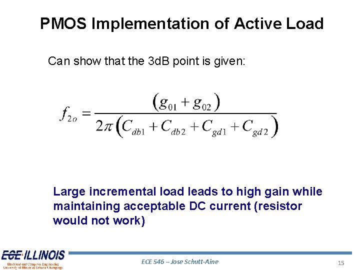
PMOS Implementation of Active Load Can show that the 3 d. B point is given: Large incremental load leads to high gain while maintaining acceptable DC current (resistor would not work) ECE 546 – Jose Schutt-Aine 15

Background • Differential Amplifiers – The input stage of every op amp is a differential amplifier – Immunity to temperature effects – Ability to amplify dc signals – Well-suited for IC fabrication because – (a) they depend on matching of elements – (b) they use more components – Less sensitive to noise and interference – Enable to bias amplifier and connect to other stage without the use of coupling capacitors ECE 546 – Jose Schutt-Aine 16

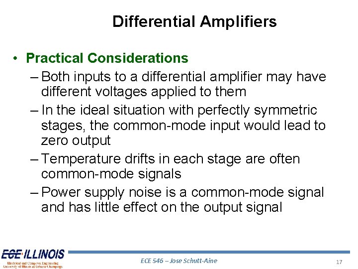
Differential Amplifiers • Practical Considerations – Both inputs to a differential amplifier may have different voltages applied to them – In the ideal situation with perfectly symmetric stages, the common-mode input would lead to zero output – Temperature drifts in each stage are often common-mode signals – Power supply noise is a common-mode signal and has little effect on the output signal ECE 546 – Jose Schutt-Aine 17

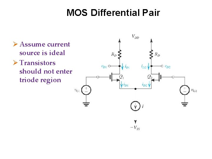
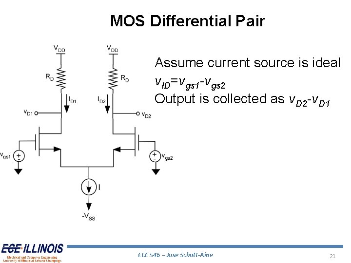
MOS Differential Pair Ø Assume current source is ideal Ø Transistors should not enter triode region

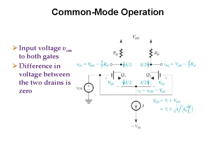
Common-Mode Operation Ø Input voltage vcm to both gates Ø Difference in voltage between the two drains is zero

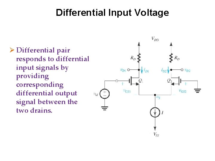
Differential Input Voltage Ø Differential pair responds to differntial input signals by providing corresponding differential output signal between the two drains.

MOS Differential Pair Assume current source is ideal v. ID=vgs 1 -vgs 2 Output is collected as v. D 2 -v. D 1 ECE 546 – Jose Schutt-Aine 21

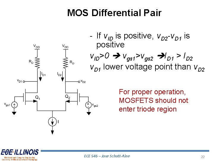
MOS Differential Pair - If v. ID is positive, v. D 2 -v. D 1 is positive v. ID>0 vgs 1>vgs 2 ID 1 > ID 2 v. D 1 lower voltage point than v. D 2 For properation, MOSFETS should not enter triode region ECE 546 – Jose Schutt-Aine 22

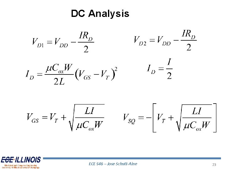
DC Analysis ECE 546 – Jose Schutt-Aine 23

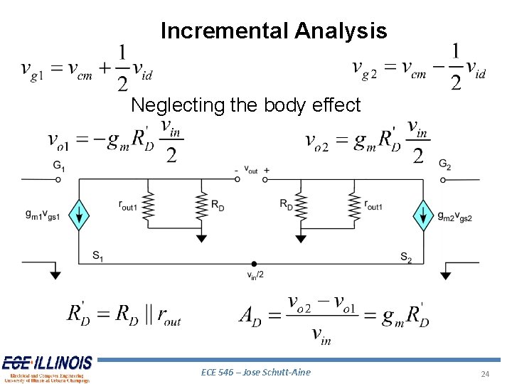
Incremental Analysis Neglecting the body effect ECE 546 – Jose Schutt-Aine 24

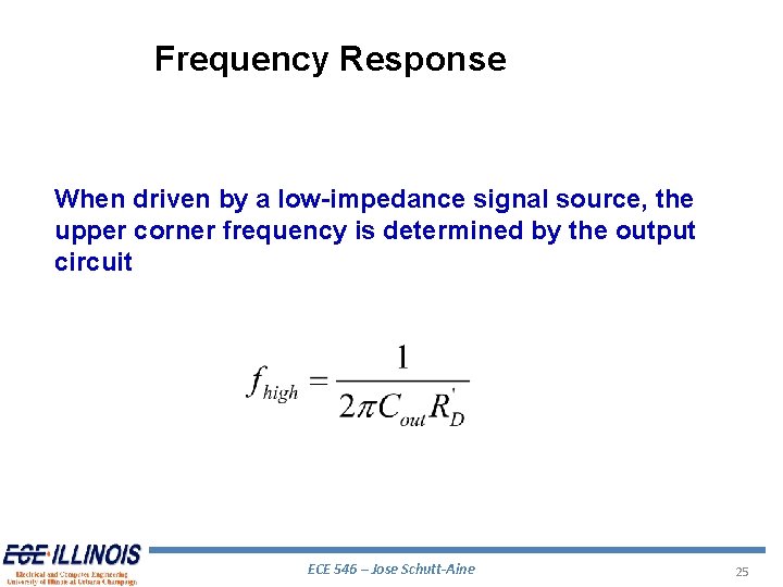
Frequency Response When driven by a low-impedance signal source, the upper corner frequency is determined by the output circuit ECE 546 – Jose Schutt-Aine 25

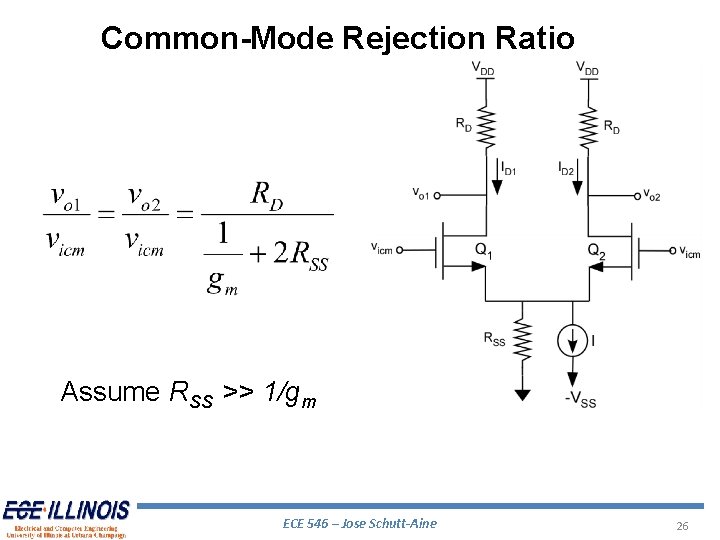
Common-Mode Rejection Ratio Assume RSS >> 1/gm ECE 546 – Jose Schutt-Aine 26

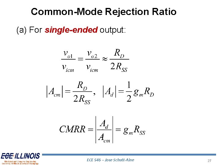
Common-Mode Rejection Ratio (a) For single-ended output: ECE 546 – Jose Schutt-Aine 27

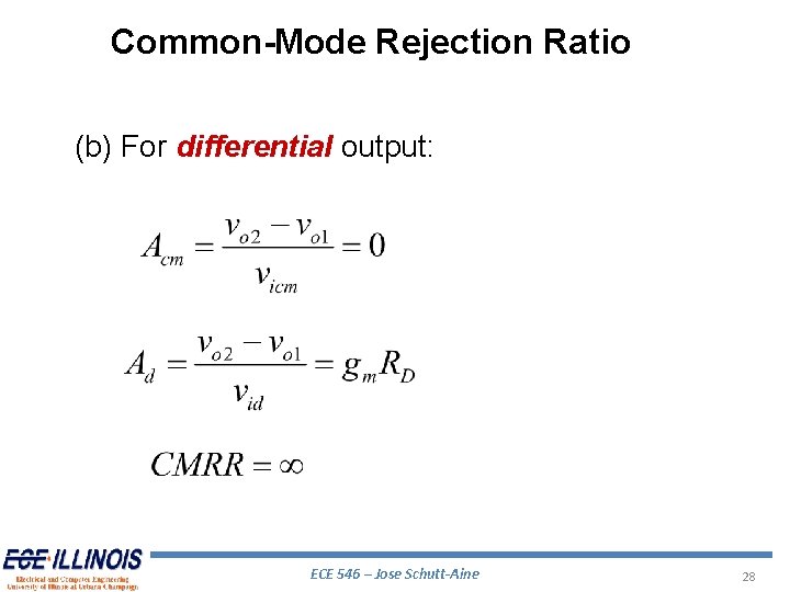
Common-Mode Rejection Ratio (b) For differential output: ECE 546 – Jose Schutt-Aine 28

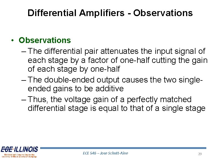
Differential Amplifiers - Observations • Observations – The differential pair attenuates the input signal of each stage by a factor of one-half cutting the gain of each stage by one-half – The double-ended output causes the two singleended gains to be additive – Thus, the voltage gain of a perfectly matched differential stage is equal to that of a single stage ECE 546 – Jose Schutt-Aine 29

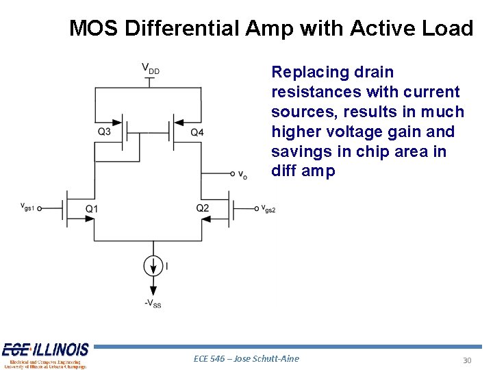
MOS Differential Amp with Active Load Replacing drain resistances with current sources, results in much higher voltage gain and savings in chip area in diff amp ECE 546 – Jose Schutt-Aine 30

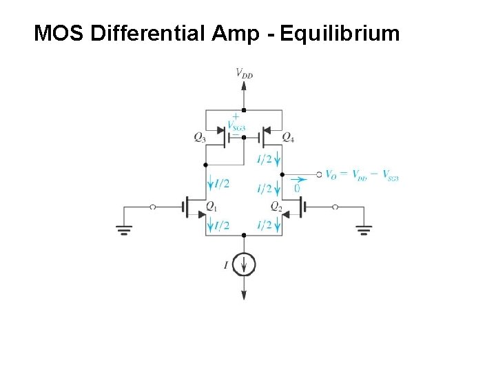
MOS Differential Amp - Equilibrium

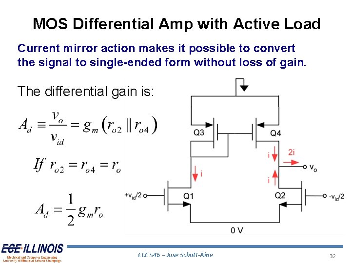
MOS Differential Amp with Active Load Current mirror action makes it possible to convert the signal to single-ended form without loss of gain. The differential gain is: ECE 546 – Jose Schutt-Aine 32

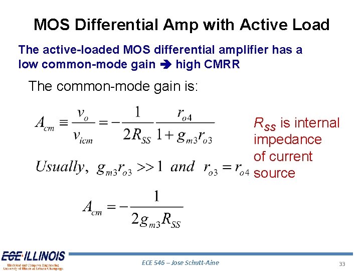
MOS Differential Amp with Active Load The active-loaded MOS differential amplifier has a low common-mode gain high CMRR The common-mode gain is: RSS is internal impedance of current source ECE 546 – Jose Schutt-Aine 33

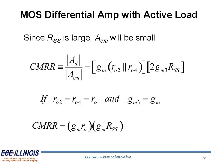
MOS Differential Amp with Active Load Since RSS is large, Acm will be small ECE 546 – Jose Schutt-Aine 34

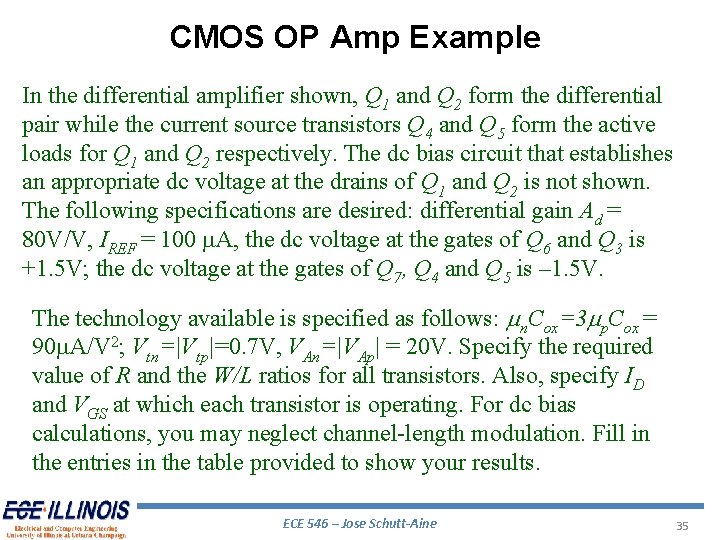
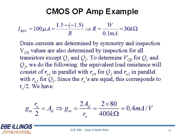
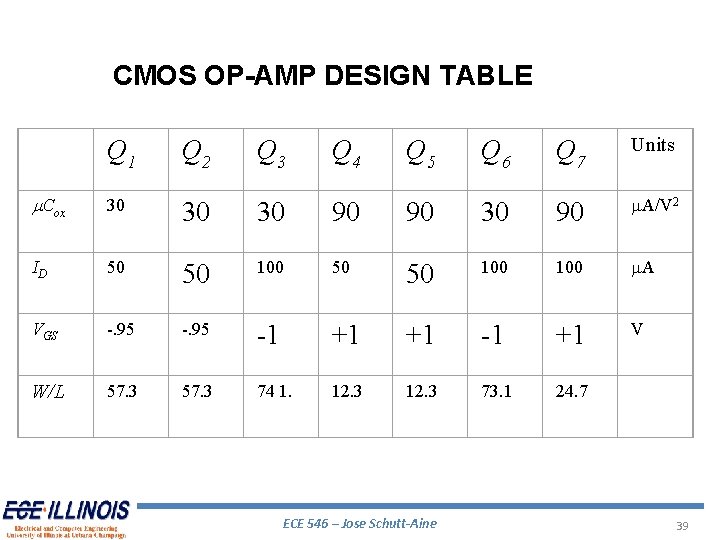
CMOS OP Amp Example In the differential amplifier shown, Q 1 and Q 2 form the differential pair while the current source transistors Q 4 and Q 5 form the active loads for Q 1 and Q 2 respectively. The dc bias circuit that establishes an appropriate dc voltage at the drains of Q 1 and Q 2 is not shown. The following specifications are desired: differential gain Ad = 80 V/V, IREF = 100 m. A, the dc voltage at the gates of Q 6 and Q 3 is +1. 5 V; the dc voltage at the gates of Q 7, Q 4 and Q 5 is – 1. 5 V. The technology available is specified as follows: mn. Cox=3 mp. Cox = 90 m. A/V 2; Vtn=|Vtp|=0. 7 V, VAn=|VAp| = 20 V. Specify the required value of R and the W/L ratios for all transistors. Also, specify ID and VGS at which each transistor is operating. For dc bias calculations, you may neglect channel-length modulation. Fill in the entries in the table provided to show your results. ECE 546 – Jose Schutt-Aine 35

CMOS OP Amp Example ECE 546 – Jose Schutt-Aine 36

CMOS OP Amp Example Drain currents are determined by symmetry and inspection VGS values are also determined by inspection for all transistors except Q 1 and Q 2. To determine VGS for Q 1 and Q 2, we do the following: the equivalent load resistance will consist of ro 1 in parallel with ro 4 for Q 1 and ro 2 in parallel with ro 5 for Q 5. Since the ro’s are equal, this corresponds to ro/2. We have: ECE 546 – Jose Schutt-Aine 37

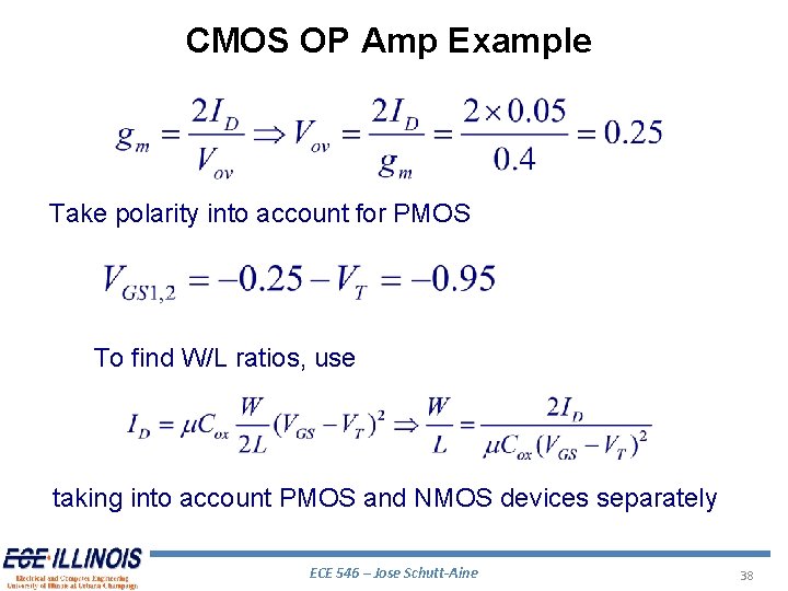
CMOS OP Amp Example Take polarity into account for PMOS To find W/L ratios, use taking into account PMOS and NMOS devices separately ECE 546 – Jose Schutt-Aine 38

CMOS OP-AMP DESIGN TABLE Q 1 m. Cox 30 30 30 90 90 ID 50 50 100 50 VGS -. 95 -1 W/L 57. 3 74 1. Q 2 Q 3 Q 7 Units 30 90 m. A/V 2 50 100 m. A +1 +1 -1 +1 V 12. 3 73. 1 24. 7 Q 4 Q 5 ECE 546 – Jose Schutt-Aine Q 6 39