ECE 546 Lecture 10 MOS Transistors Spring 2018
- Slides: 42

ECE 546 Lecture 10 MOS Transistors Spring 2018 Jose E. Schutt-Aine Electrical & Computer Engineering University of Illinois jesa@illinois. edu ECE 546 – Jose Schutt-Aine

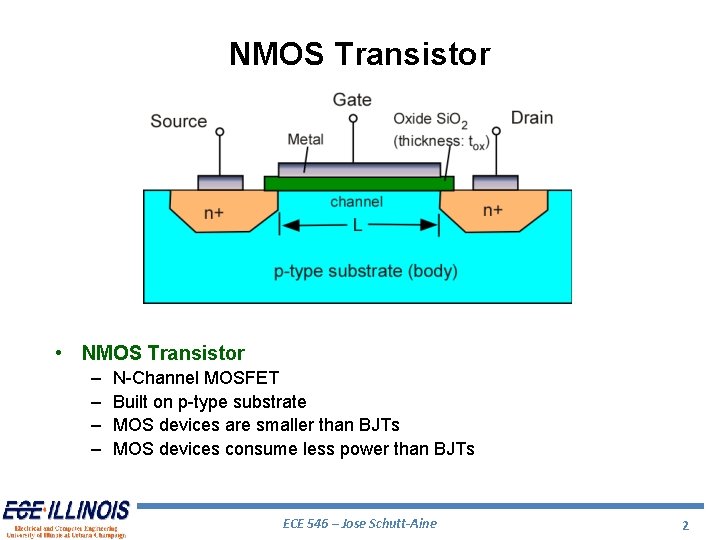
NMOS Transistor • NMOS Transistor – – N-Channel MOSFET Built on p-type substrate MOS devices are smaller than BJTs MOS devices consume less power than BJTs ECE 546 – Jose Schutt-Aine 2

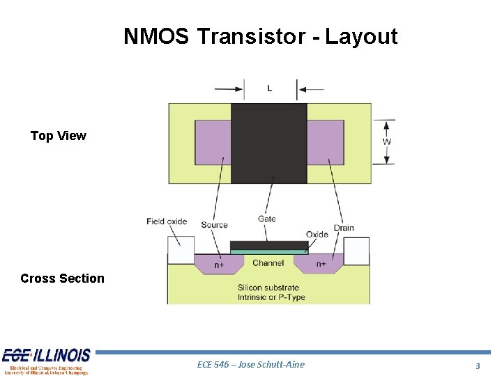
NMOS Transistor - Layout Top View Cross Section ECE 546 – Jose Schutt-Aine 3

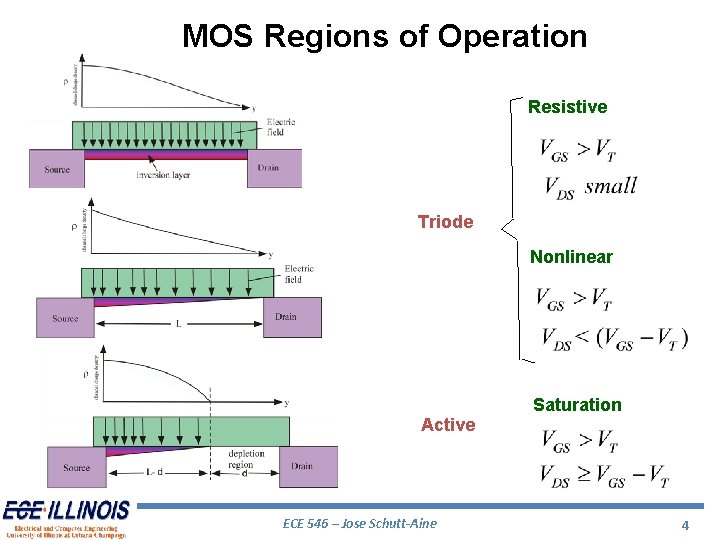
MOS Regions of Operation Resistive Triode Nonlinear Active ECE 546 – Jose Schutt-Aine Saturation 4

MOS Transistor Operation • As VG increases from zero – Holes in the p substrate are repelled from the gate area leaving negative ions behind – A depletion region is created – No current flows since no carriers are available • As VG increases – The width of the depletion region and the potential at the oxide-silicon interface also increase – When the interface potential reaches a sufficiently positive value, electrons flow in the “channel”. The transistor is turned on • As VG rises further – The charge in the depletion region remains relatively constant – The channel current continues to increase ECE 546 – Jose Schutt-Aine 5

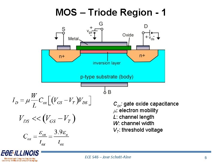
MOS – Triode Region - 1 Cox: gate oxide capacitance m: electron mobility L: channel length W: channel width VT: threshold voltage ECE 546 – Jose Schutt-Aine 6

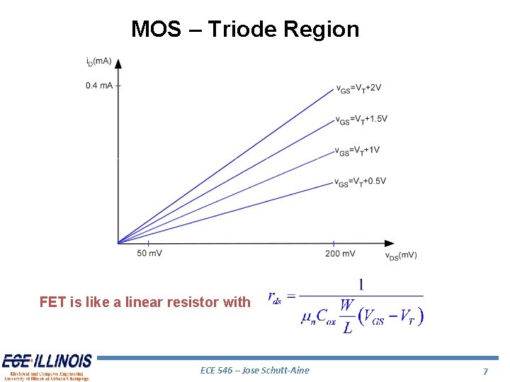
MOS – Triode Region FET is like a linear resistor with ECE 546 – Jose Schutt-Aine 7

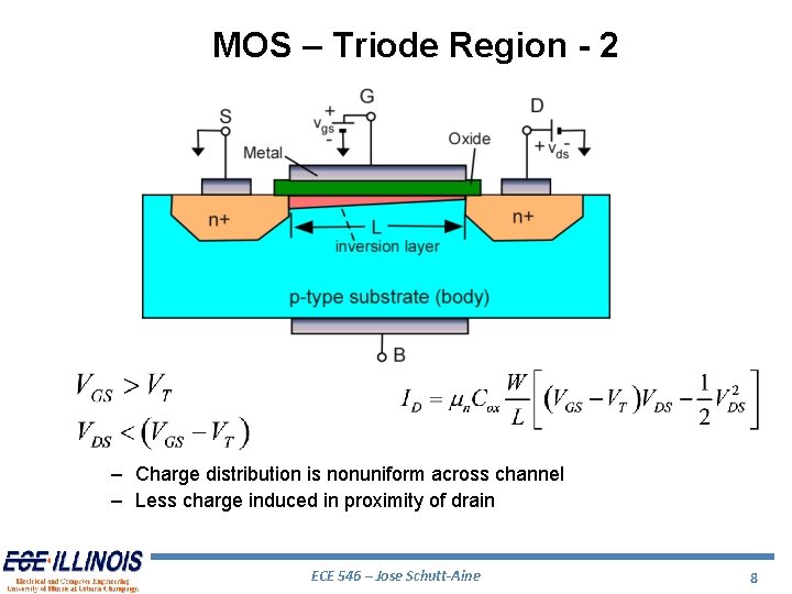
MOS – Triode Region - 2 – Charge distribution is nonuniform across channel – Less charge induced in proximity of drain ECE 546 – Jose Schutt-Aine 8

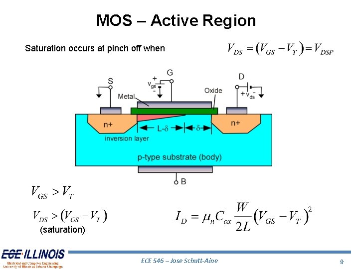
MOS – Active Region Saturation occurs at pinch off when (saturation) ECE 546 – Jose Schutt-Aine 9

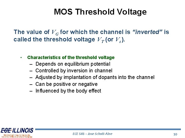
MOS Threshold Voltage The value of VG for which the channel is “inverted” is called the threshold voltage VT (or Vt ). • Characteristics of the threshold voltage – – – Depends on equilibrium potential Controlled by inversion in channel Adjusted by implantation of dopants into the channel Can be positive or negative Influenced by the body effect ECE 546 – Jose Schutt-Aine 10

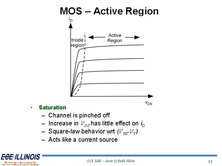
MOS – Active Region • Saturation – – Channel is pinched off Increase in VDS has little effect on i. D Square-law behavior wrt (VGS-VT) Acts like a current source ECE 546 – Jose Schutt-Aine 11

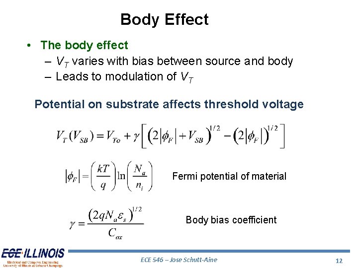
Body Effect • The body effect – VT varies with bias between source and body – Leads to modulation of VT Potential on substrate affects threshold voltage Fermi potential of material Body bias coefficient ECE 546 – Jose Schutt-Aine 12

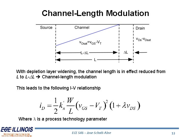
Channel-Length Modulation With depletion layer widening, the channel length is in effect reduced from L to L-DL Channel-length modulation This leads to the following I-V relationship Where l is a process technology parameter ECE 546 – Jose Schutt-Aine 13

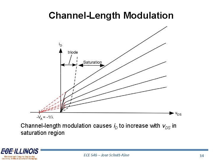
Channel-Length Modulation Channel-length modulation causes i. D to increase with v. DS in saturation region ECE 546 – Jose Schutt-Aine 14

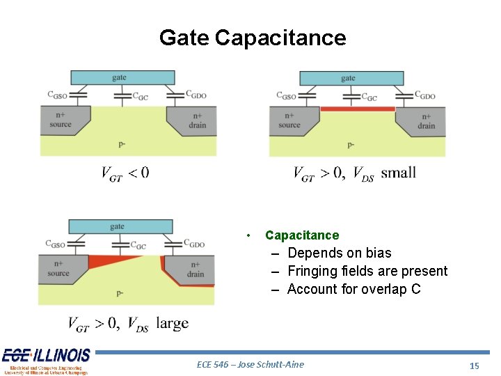
Gate Capacitance • Capacitance – Depends on bias – Fringing fields are present – Account for overlap C ECE 546 – Jose Schutt-Aine 15

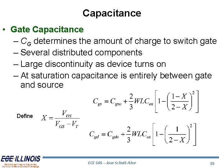
Capacitance • Gate Capacitance – CG determines the amount of charge to switch gate – Several distributed components – Large discontinuity as device turns on – At saturation capacitance is entirely between gate and source Define ECE 546 – Jose Schutt-Aine 16

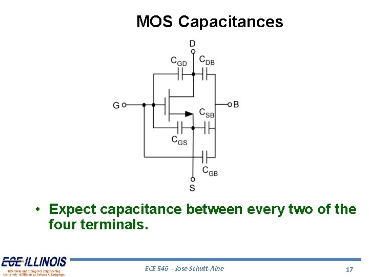
MOS Capacitances • Expect capacitance between every two of the four terminals. ECE 546 – Jose Schutt-Aine 17

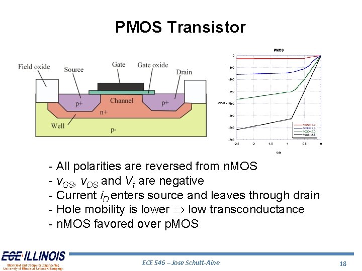
PMOS Transistor - All polarities are reversed from n. MOS - v. GS, v. DS and Vt are negative - Current i. D enters source and leaves through drain - Hole mobility is lower low transconductance - n. MOS favored over p. MOS ECE 546 – Jose Schutt-Aine 18

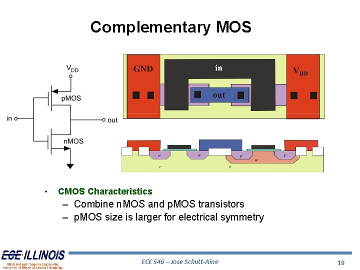
Complementary MOS • CMOS Characteristics – Combine n. MOS and p. MOS transistors – p. MOS size is larger for electrical symmetry ECE 546 – Jose Schutt-Aine 19

CMOS • Advantages – Virtually, no DC power consumed – No DC path between power and ground – Excellent noise margins (VOL=0, VOH=VDD) – Inverter has sharp transfer curve • Drawbacks – Requires more transistors – Process is more complicated – p. MOS size larger to achieve electrical symmetry – Latch up ECE 546 – Jose Schutt-Aine 20

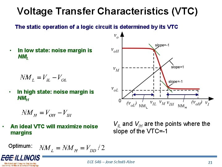
Voltage Transfer Characteristics (VTC) The static operation of a logic circuit is determined by its VTC • In low state: noise margin is NML • In high state: noise margin is NMH NML • An ideal VTC will maximize noise margins NMH VIL and VIH are the points where the slope of the VTC=-1 Optimum: ECE 546 – Jose Schutt-Aine 21

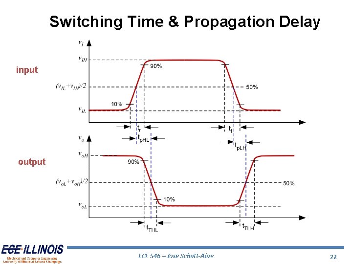
Switching Time & Propagation Delay input output ECE 546 – Jose Schutt-Aine 22

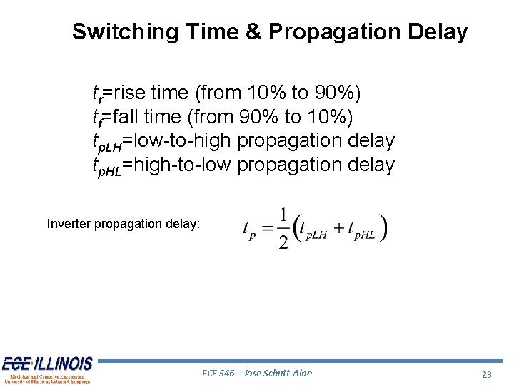
Switching Time & Propagation Delay tr=rise time (from 10% to 90%) tf=fall time (from 90% to 10%) tp. LH=low-to-high propagation delay tp. HL=high-to-low propagation delay Inverter propagation delay: ECE 546 – Jose Schutt-Aine 23

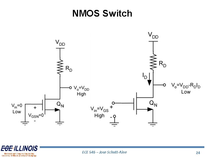
NMOS Switch ECE 546 – Jose Schutt-Aine 24

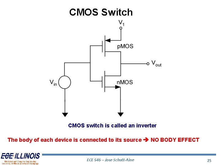
CMOS Switch CMOS switch is called an inverter The body of each device is connected to its source NO BODY EFFECT ECE 546 – Jose Schutt-Aine 25

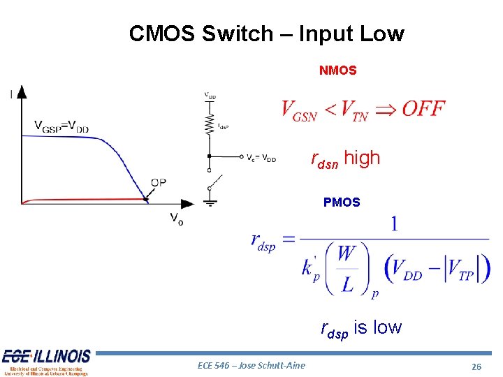
CMOS Switch – Input Low NMOS rdsn high PMOS rdsp is low ECE 546 – Jose Schutt-Aine 26

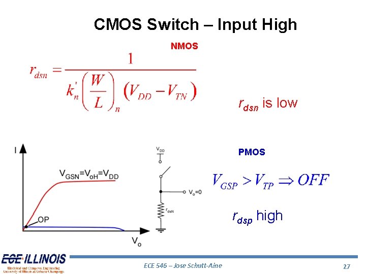
CMOS Switch – Input High NMOS rdsn is low PMOS rdsp high ECE 546 – Jose Schutt-Aine 27

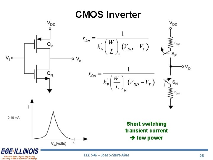
CMOS Inverter Short switching transient current low power ECE 546 – Jose Schutt-Aine 28

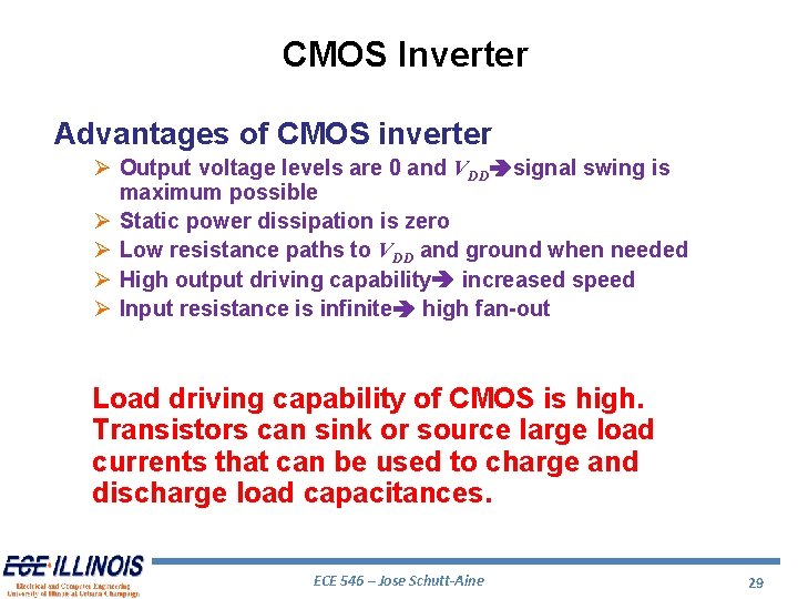
CMOS Inverter Advantages of CMOS inverter Ø Output voltage levels are 0 and VDD signal swing is maximum possible Ø Static power dissipation is zero Ø Low resistance paths to VDD and ground when needed Ø High output driving capability increased speed Ø Input resistance is infinite high fan-out Load driving capability of CMOS is high. Transistors can sink or source large load currents that can be used to charge and discharge load capacitances. ECE 546 – Jose Schutt-Aine 29

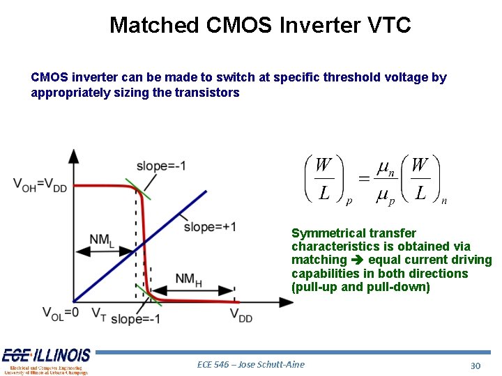
Matched CMOS Inverter VTC CMOS inverter can be made to switch at specific threshold voltage by appropriately sizing the transistors Symmetrical transfer characteristics is obtained via matching equal current driving capabilities in both directions (pull-up and pull-down) ECE 546 – Jose Schutt-Aine 30

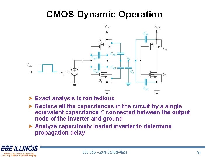
CMOS Dynamic Operation Ø Exact analysis is too tedious Ø Replace all the capacitances in the circuit by a single equivalent capacitance C connected between the output node of the inverter and ground Ø Analyze capacitively loaded inverter to determine propagation delay ECE 546 – Jose Schutt-Aine 31

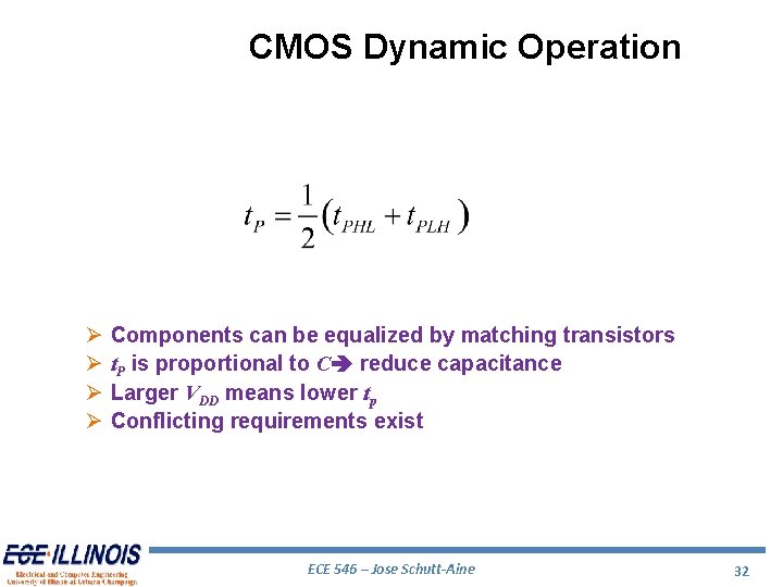
CMOS Dynamic Operation Ø Ø Components can be equalized by matching transistors t. P is proportional to C reduce capacitance Larger VDD means lower tp Conflicting requirements exist ECE 546 – Jose Schutt-Aine 32

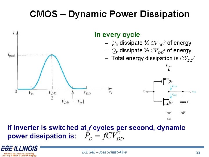
CMOS – Dynamic Power Dissipation In every cycle – QN dissipate ½ CVDD 2 of energy – QP dissipate ½ CVDD 2 of energy – Total energy dissipation is CVDD 2 If inverter is switched at f cycles per second, dynamic power dissipation is: ECE 546 – Jose Schutt-Aine 33

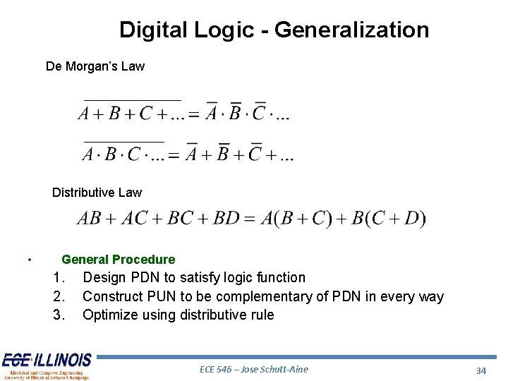
Digital Logic - Generalization De Morgan’s Law Distributive Law • General Procedure 1. 2. 3. Design PDN to satisfy logic function Construct PUN to be complementary of PDN in every way Optimize using distributive rule ECE 546 – Jose Schutt-Aine 34

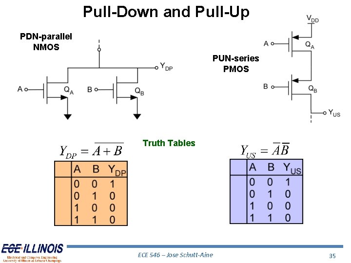
Pull-Down and Pull-Up PDN-parallel NMOS PUN-series PMOS Truth Tables ECE 546 – Jose Schutt-Aine 35

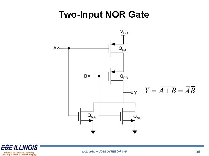
Two-Input NOR Gate ECE 546 – Jose Schutt-Aine 36

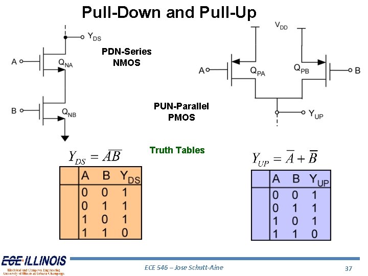
Pull-Down and Pull-Up PDN-Series NMOS PUN-Parallel PMOS Truth Tables ECE 546 – Jose Schutt-Aine 37

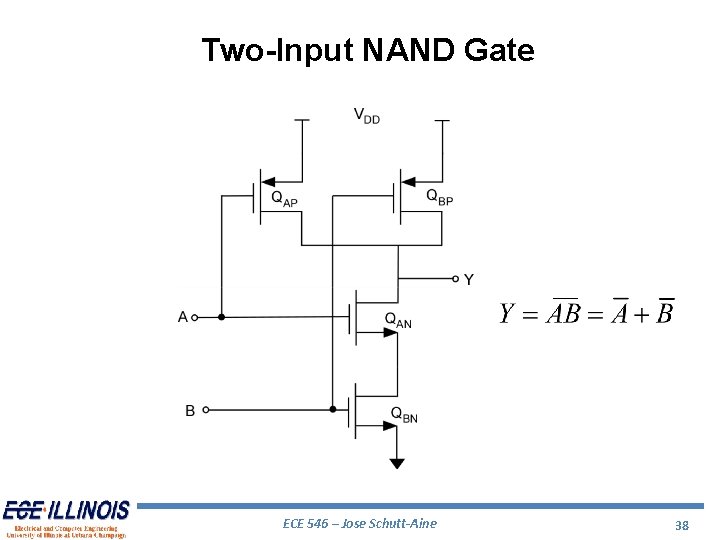
Two-Input NAND Gate ECE 546 – Jose Schutt-Aine 38

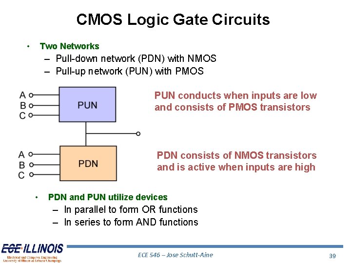
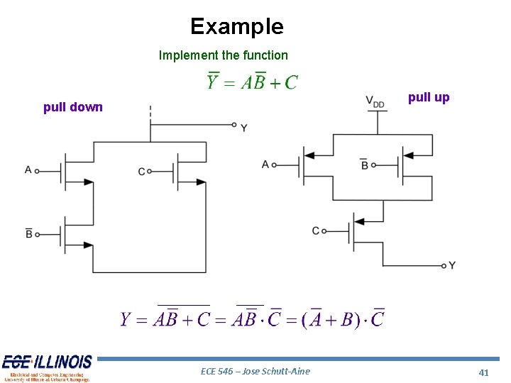
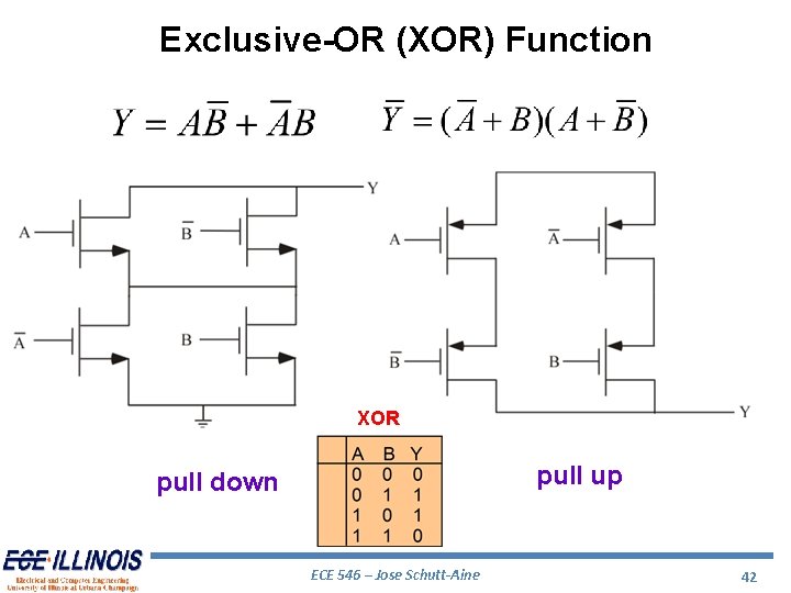
CMOS Logic Gate Circuits • Two Networks – Pull-down network (PDN) with NMOS – Pull-up network (PUN) with PMOS PUN conducts when inputs are low and consists of PMOS transistors PDN consists of NMOS transistors and is active when inputs are high • PDN and PUN utilize devices – In parallel to form OR functions – In series to form AND functions ECE 546 – Jose Schutt-Aine 39

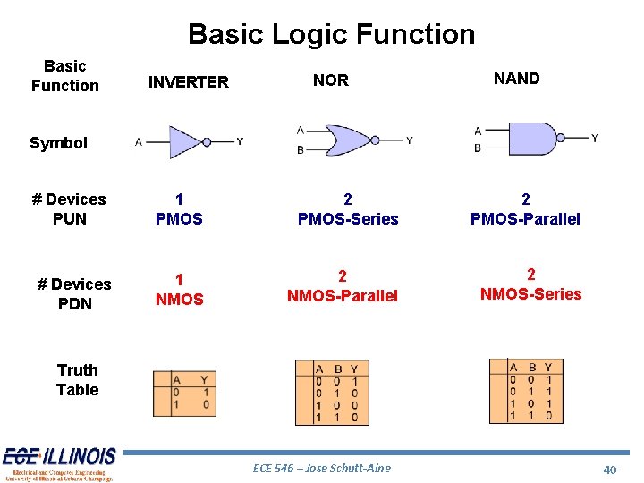
Basic Logic Function Basic Function INVERTER NOR NAND Symbol # Devices PUN # Devices PDN 1 PMOS 2 PMOS-Series 2 PMOS-Parallel 1 NMOS 2 NMOS-Parallel 2 NMOS-Series Truth Table ECE 546 – Jose Schutt-Aine 40

Example Implement the function pull up pull down ECE 546 – Jose Schutt-Aine 41

Exclusive-OR (XOR) Function XOR pull up pull down ECE 546 – Jose Schutt-Aine 42