
ECE 546 Introduction Spring 2014 Jose E SchuttAine
- Slides: 54
ECE 546 Introduction Spring 2014 Jose E. Schutt-Aine Electrical & Computer Engineering University of Illinois jschutt@emlab. uiuc. edu ECE 546 – Jose Schutt-Aine 1
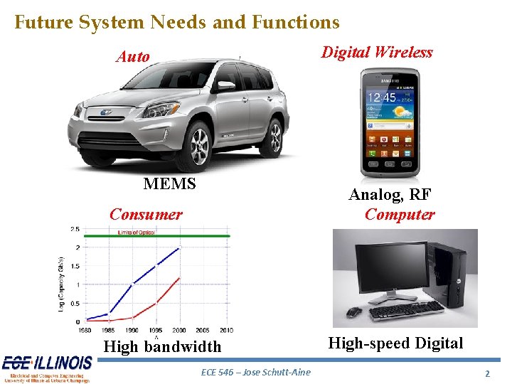
Future System Needs and Functions Digital Wireless Auto MEMS Analog, RF Computer Consumer High bandwidth ECE 546 – Jose Schutt-Aine High-speed Digital 2
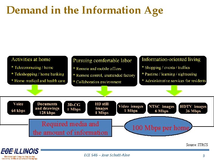
Demand in the Information Age Required media and the amount of information 100 Mbps per home Source: ITRCS ECE 546 – Jose Schutt-Aine 3
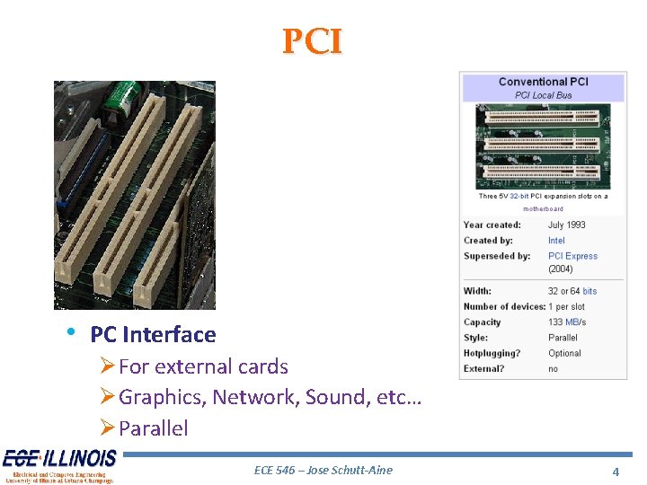
PCI • PC Interface Ø For external cards Ø Graphics, Network, Sound, etc… Ø Parallel ECE 546 – Jose Schutt-Aine 4
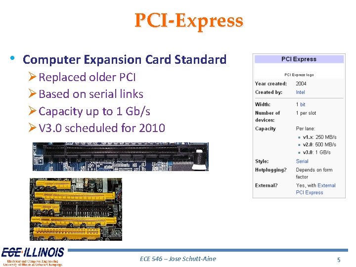
PCI-Express • Computer Expansion Card Standard Ø Replaced older PCI Ø Based on serial links Ø Capacity up to 1 Gb/s Ø V 3. 0 scheduled for 2010 ECE 546 – Jose Schutt-Aine 5
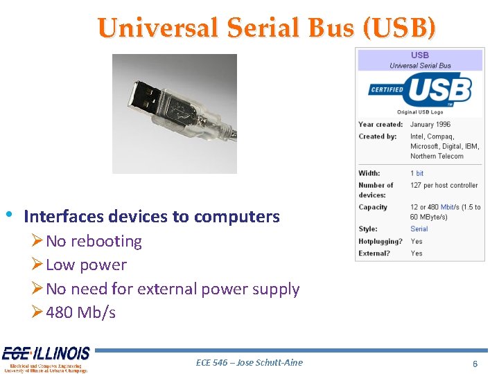
Universal Serial Bus (USB) • Interfaces devices to computers Ø No rebooting Ø Low power Ø No need for external power supply Ø 480 Mb/s ECE 546 – Jose Schutt-Aine 6
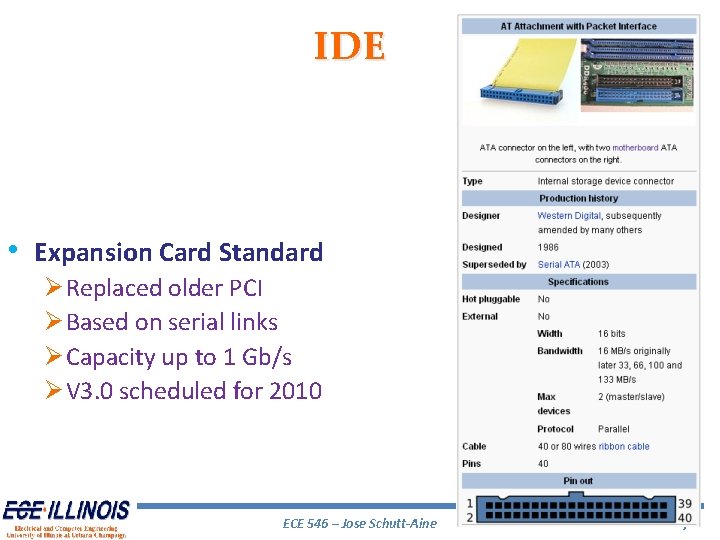
IDE • Expansion Card Standard Ø Replaced older PCI Ø Based on serial links Ø Capacity up to 1 Gb/s Ø V 3. 0 scheduled for 2010 ECE 546 – Jose Schutt-Aine 7 7
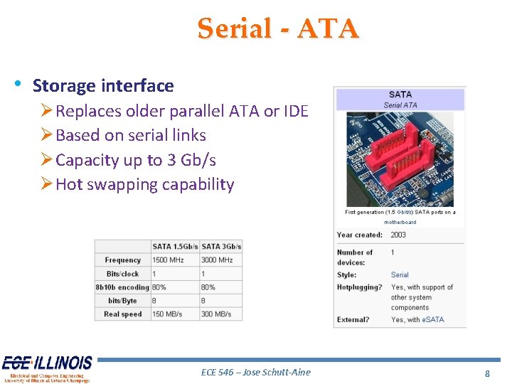
Serial - ATA • Storage interface Ø Replaces older parallel ATA or IDE Ø Based on serial links Ø Capacity up to 3 Gb/s Ø Hot swapping capability ECE 546 – Jose Schutt-Aine 8
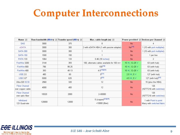
Computer Interconnections ECE 546 – Jose Schutt-Aine 9
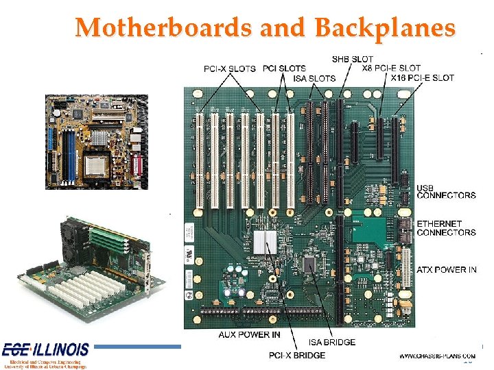
Motherboards and Backplanes ECE 546 – Jose Schutt-Aine 10 10
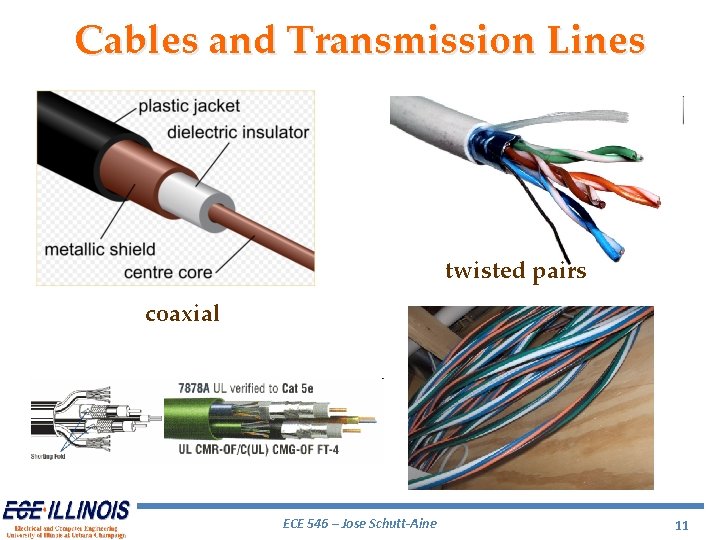
Cables and Transmission Lines twisted pairs coaxial ECE 546 – Jose Schutt-Aine 11
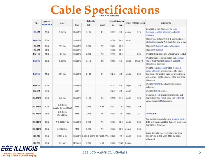
Cable Specifications ECE 546 – Jose Schutt-Aine 12
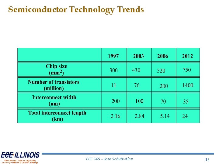
Semiconductor Technology Trends ECE 546 – Jose Schutt-Aine 13
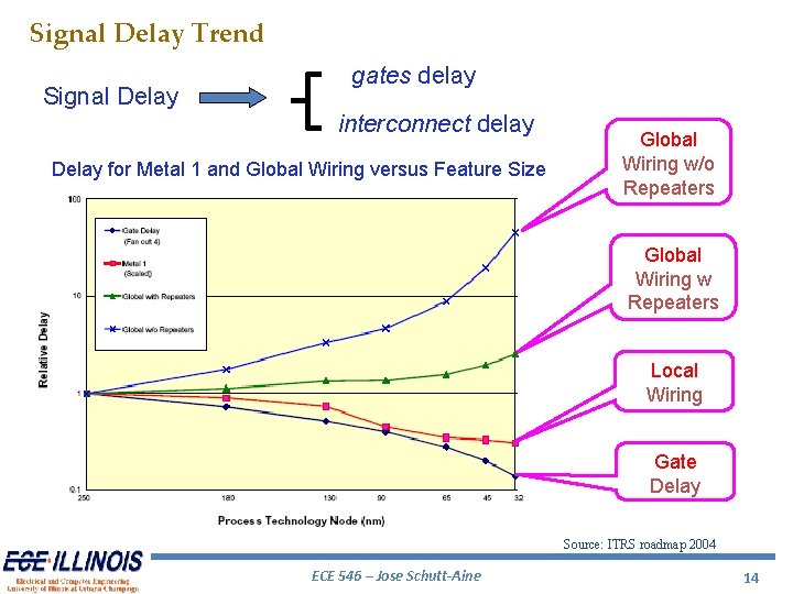
Signal Delay Trend Signal Delay gates delay interconnect delay Delay for Metal 1 and Global Wiring versus Feature Size Global Wiring w/o Repeaters Global Wiring w Repeaters Local Wiring Gate Delay Source: ITRS roadmap 2004 ECE 546 – Jose Schutt-Aine 14
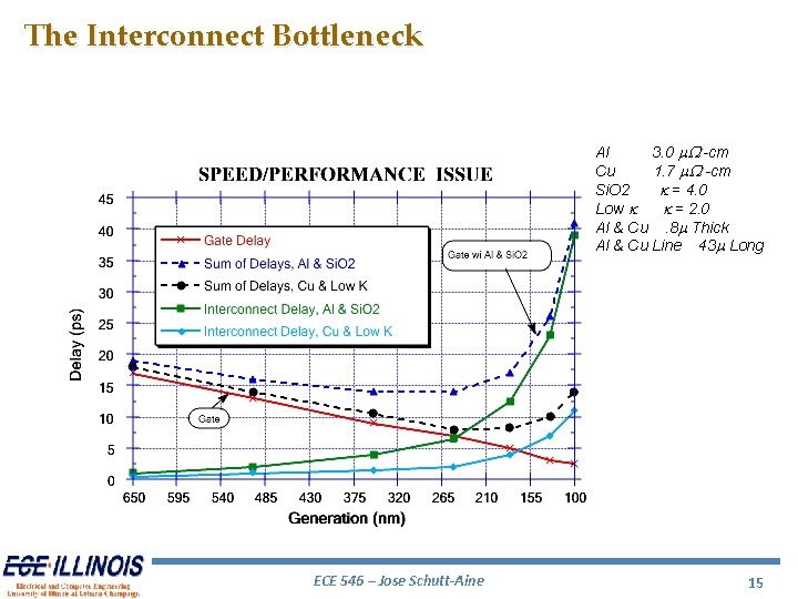
The Interconnect Bottleneck Al 3. 0 m. W -cm Cu 1. 7 m. W -cm Si. O 2 k = 4. 0 Low k k = 2. 0 Al & Cu. 8 m Thick Al & Cu Line 43 m Long ECE 546 – Jose Schutt-Aine 15
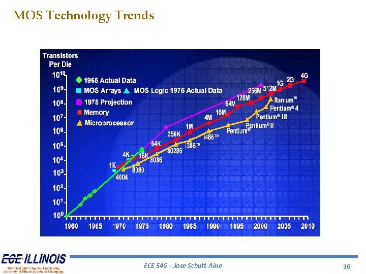
MOS Technology Trends ECE 546 – Jose Schutt-Aine 16
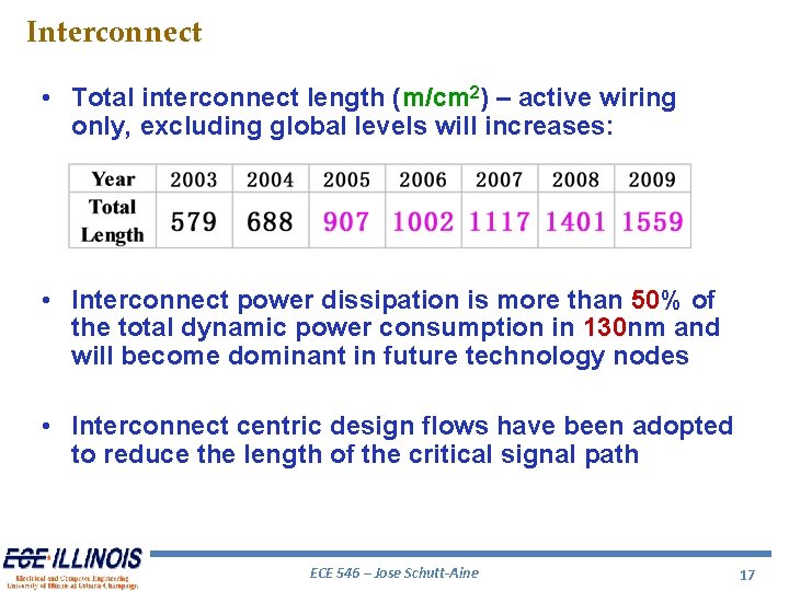
Interconnect • Total interconnect length (m/cm 2) – active wiring only, excluding global levels will increases: • Interconnect power dissipation is more than 50% of the total dynamic power consumption in 130 nm and will become dominant in future technology nodes • Interconnect centric design flows have been adopted to reduce the length of the critical signal path ECE 546 – Jose Schutt-Aine 17
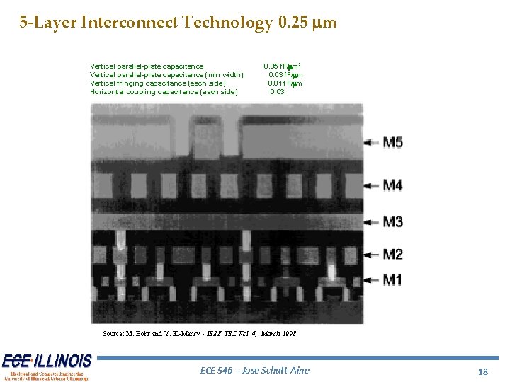
5 -Layer Interconnect Technology 0. 25 mm Vertical parallel-plate capacitance (min width) Vertical fringing capacitance (each side) Horizontal coupling capacitance (each side) 0. 05 f. F/mm 2 0. 03 f. F/mm 0. 01 f. F/mm 0. 03 Source: M. Bohr and Y. El-Mansy - IEEE TED Vol. 4, March 1998 ECE 546 – Jose Schutt-Aine 18
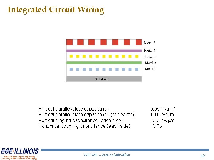
Integrated Circuit Wiring Vertical parallel-plate capacitance (min width) Vertical fringing capacitance (each side) Horizontal coupling capacitance (each side) ECE 546 – Jose Schutt-Aine 0. 05 f. F/mm 2 0. 03 f. F/mm 0. 01 f. F/mm 0. 03 19
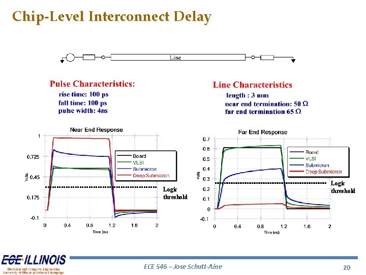
Chip-Level Interconnect Delay Logic threshold ECE 546 – Jose Schutt-Aine Logic threshold 20
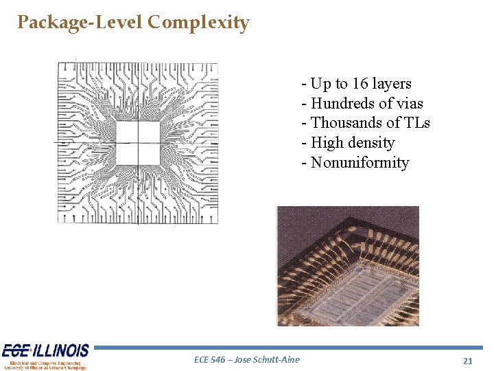
Package-Level Complexity - Up to 16 layers - Hundreds of vias - Thousands of TLs - High density - Nonuniformity ECE 546 – Jose Schutt-Aine 21
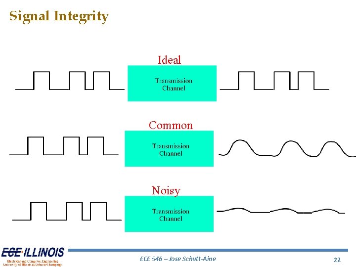
Signal Integrity Ideal Common Noisy ECE 546 – Jose Schutt-Aine 22
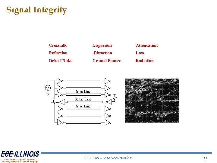
Signal Integrity Crosstalk Dispersion Attenuation Reflection Distortion Loss Delta I Noise Ground Bounce Radiation ECE 546 – Jose Schutt-Aine 23
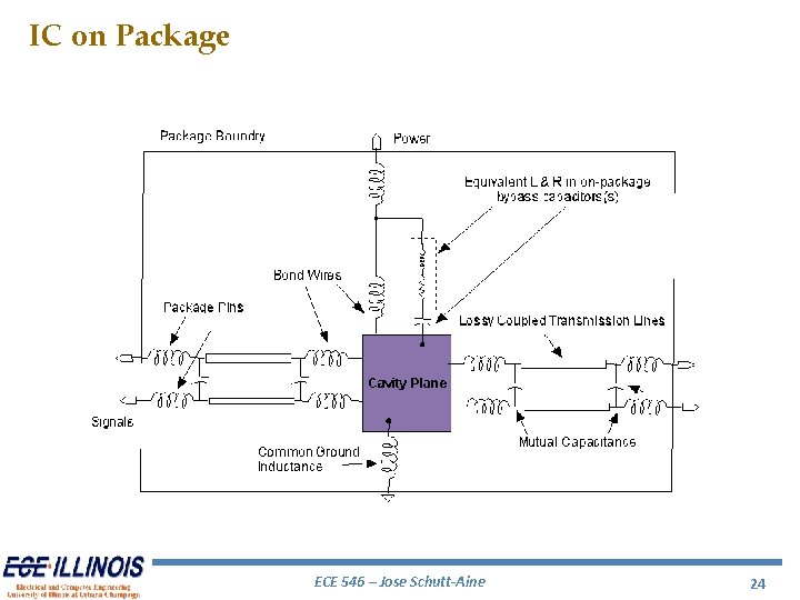
IC on Package ECE 546 – Jose Schutt-Aine 24
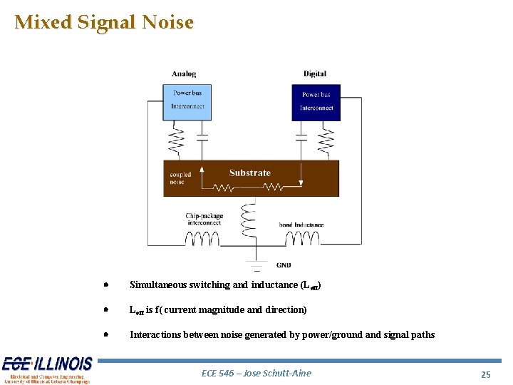
Mixed Signal Noise Simultaneous switching and inductance (Leff) Leff is f( current magnitude and direction) Interactions between noise generated by power/ground and signal paths ECE 546 – Jose Schutt-Aine 25
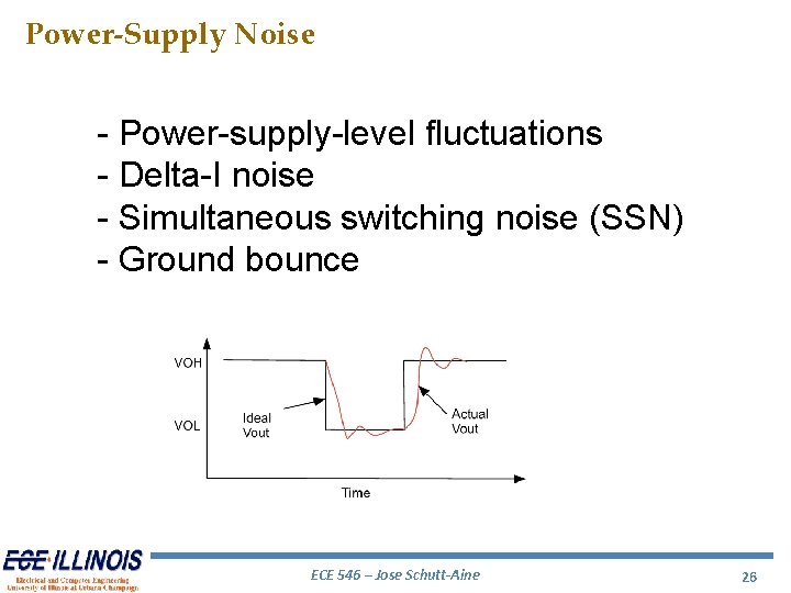
Power-Supply Noise - Power-supply-level fluctuations - Delta-I noise - Simultaneous switching noise (SSN) - Ground bounce ECE 546 – Jose Schutt-Aine 26
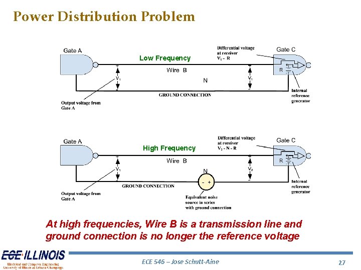
Power Distribution Problem Low Frequency High Frequency At high frequencies, Wire B is a transmission line and ground connection is no longer the reference voltage ECE 546 – Jose Schutt-Aine 27
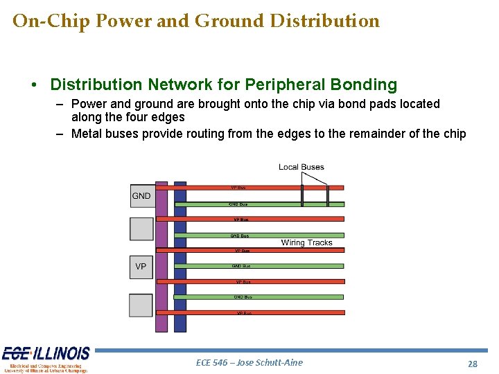
On-Chip Power and Ground Distribution • Distribution Network for Peripheral Bonding – Power and ground are brought onto the chip via bond pads located along the four edges – Metal buses provide routing from the edges to the remainder of the chip ECE 546 – Jose Schutt-Aine 28
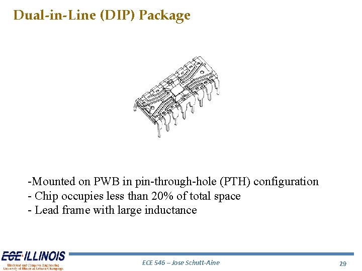
Dual-in-Line (DIP) Package -Mounted on PWB in pin-through-hole (PTH) configuration - Chip occupies less than 20% of total space - Lead frame with large inductance ECE 546 – Jose Schutt-Aine 29
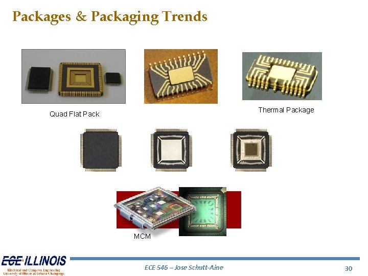
Packages & Packaging Trends Thermal Package Quad Flat Pack MCM ECE 546 – Jose Schutt-Aine 30
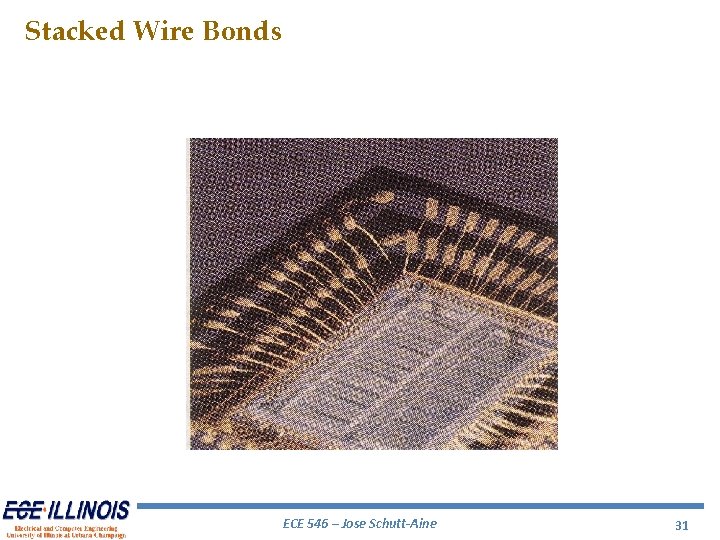
Stacked Wire Bonds ECE 546 – Jose Schutt-Aine 31
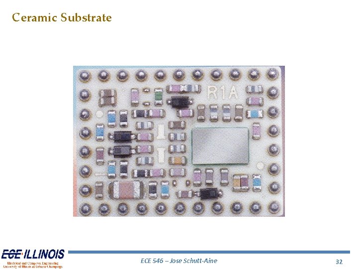
Ceramic Substrate ECE 546 – Jose Schutt-Aine 32
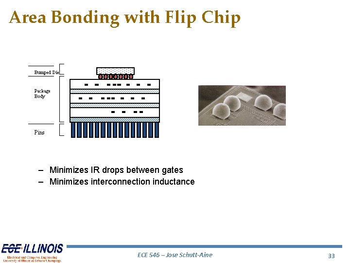
Area Bonding with Flip Chip Bumped Die Package Body Pins – Minimizes IR drops between gates – Minimizes interconnection inductance ECE 546 – Jose Schutt-Aine 33
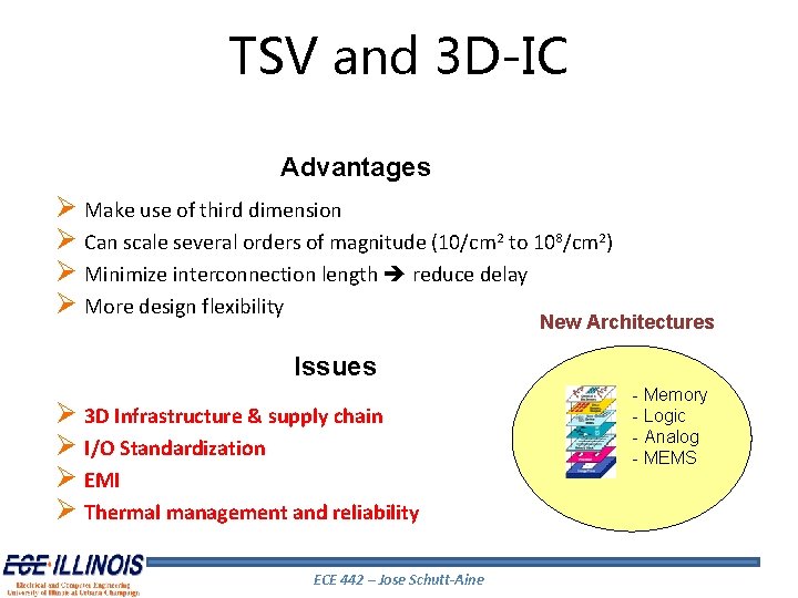
3 D IC and TSV ØMake use of third dimension ØCan scale several orders of magnitude (10/cm 2 to 108/cm 2) ØMinimize interconnection length reduce delay ØMore design flexibility ECE 546 – Jose Schutt-Aine 34
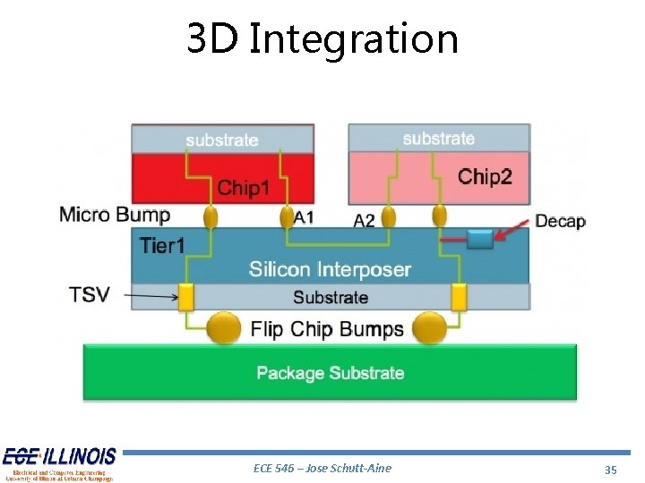
3 D Integration ECE 546 – Jose Schutt-Aine 35
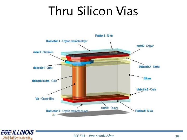
Thru Silicon Vias ECE 546 – Jose Schutt-Aine 36
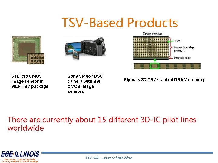
TSV-Based Products STMicro CMOS image sensor in WLP/TSV package Sony Video / DSC camera with BSI CMOS image sensors Elpida’s 3 D TSV stacked DRAM memory There are currently about 15 different 3 D-IC pilot lines worldwide ECE 546 – Jose Schutt-Aine
TSV and 3 D-IC Advantages Ø Make use of third dimension Ø Can scale several orders of magnitude (10/cm 2 to 108/cm 2) Ø Minimize interconnection length reduce delay Ø More design flexibility New Architectures Issues Ø 3 D Infrastructure & supply chain Ø I/O Standardization Ø EMI Ø Thermal management and reliability ECE 442 – Jose Schutt-Aine - Memory - Logic - Analog - MEMS
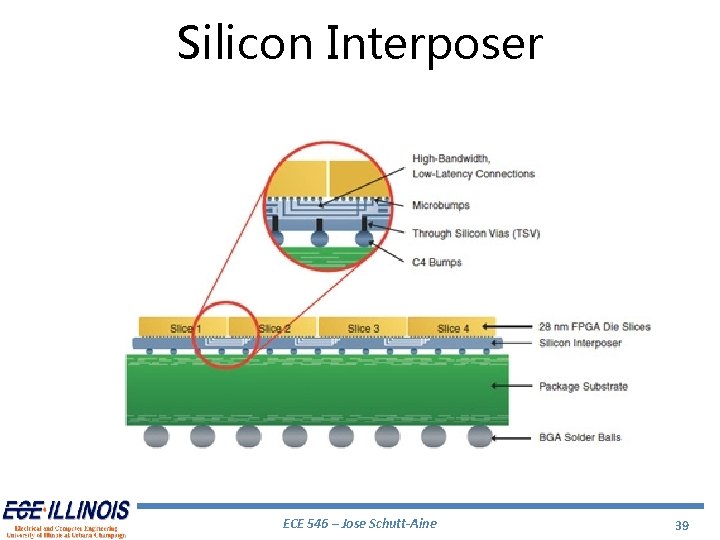
Silicon Interposer ECE 546 – Jose Schutt-Aine 39
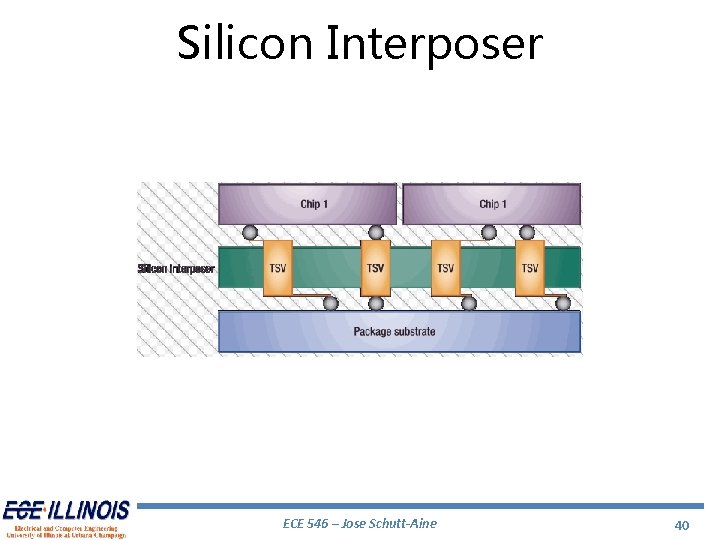
Silicon Interposer ECE 546 – Jose Schutt-Aine 40
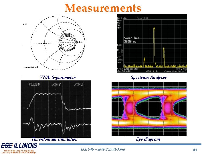
Measurements VNA: S-parameter Spectrum Analyzer Time-domain simulation Eye diagram ECE 546 – Jose Schutt-Aine 41
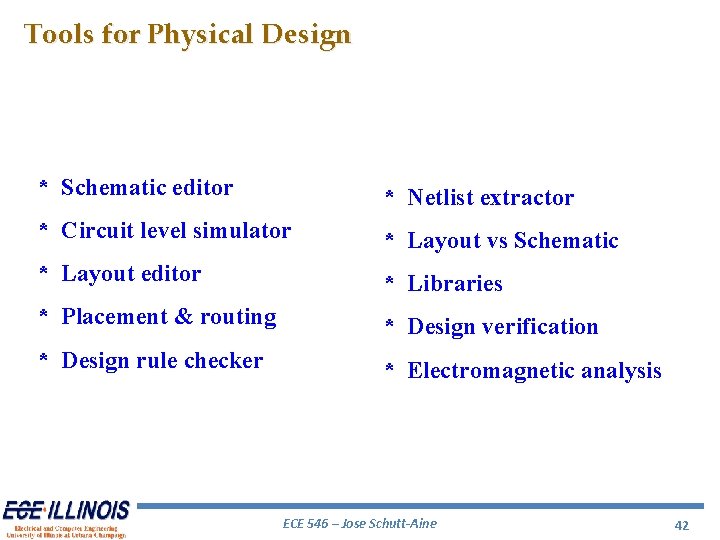
Tools for Physical Design * Schematic editor * Netlist extractor * Circuit level simulator * Layout vs Schematic * Layout editor * Libraries * Placement & routing * Design verification * Design rule checker * Electromagnetic analysis ECE 546 – Jose Schutt-Aine 42
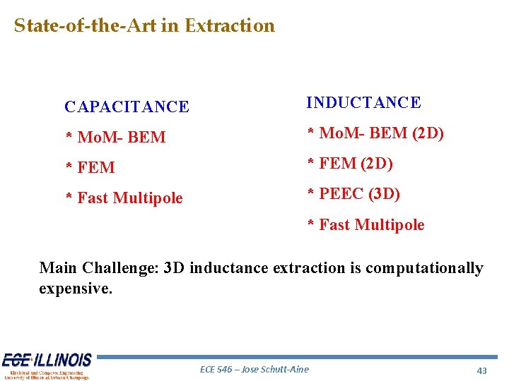
State-of-the-Art in Extraction CAPACITANCE INDUCTANCE * Mo. M- BEM (2 D) * FEM (2 D) * Fast Multipole * PEEC (3 D) * Fast Multipole Main Challenge: 3 D inductance extraction is computationally expensive. ECE 546 – Jose Schutt-Aine 43
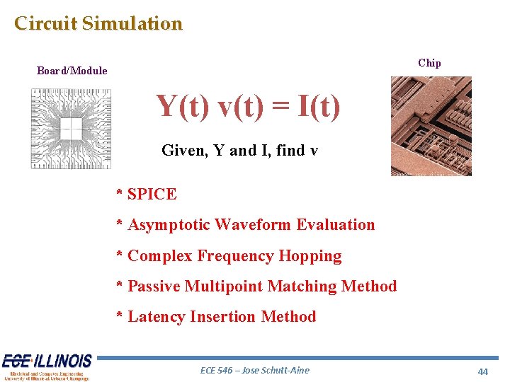
Circuit Simulation Chip Board/Module Y(t) v(t) = I(t) Given, Y and I, find v * SPICE * Asymptotic Waveform Evaluation * Complex Frequency Hopping * Passive Multipoint Matching Method * Latency Insertion Method ECE 546 – Jose Schutt-Aine 44
Why SPICE ? Established platform Powerful engine Source code available for free Extensive libraries of devices New device installation procedure straightforward ECE 546 – Jose Schutt-Aine 45
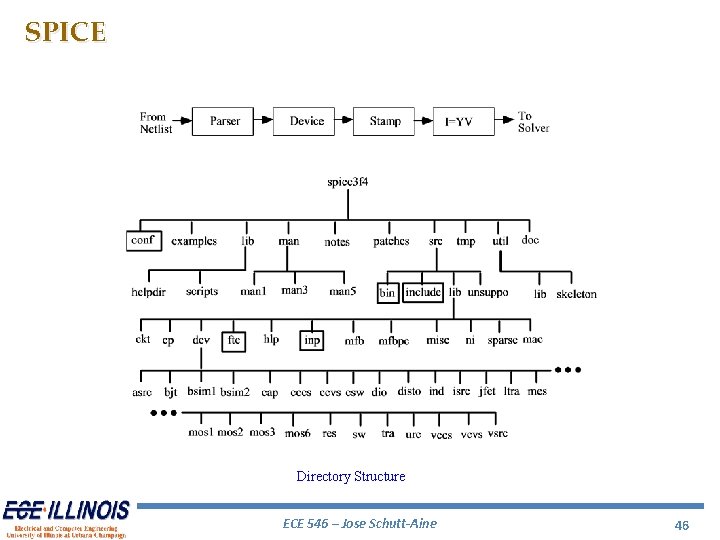
SPICE Directory Structure ECE 546 – Jose Schutt-Aine 46
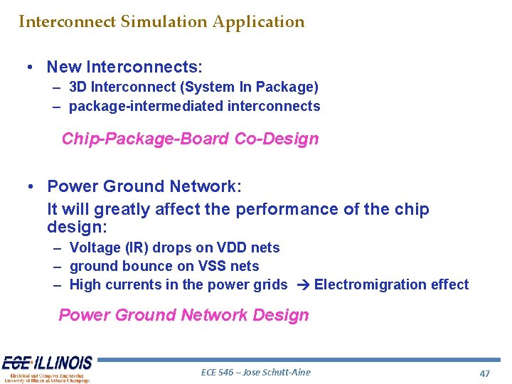
Interconnect Simulation Application • New Interconnects: – 3 D Interconnect (System In Package) – package-intermediated interconnects Chip-Package-Board Co-Design • Power Ground Network: It will greatly affect the performance of the chip design: – Voltage (IR) drops on VDD nets – ground bounce on VSS nets – High currents in the power grids Electromigration effect Power Ground Network Design ECE 546 – Jose Schutt-Aine 47
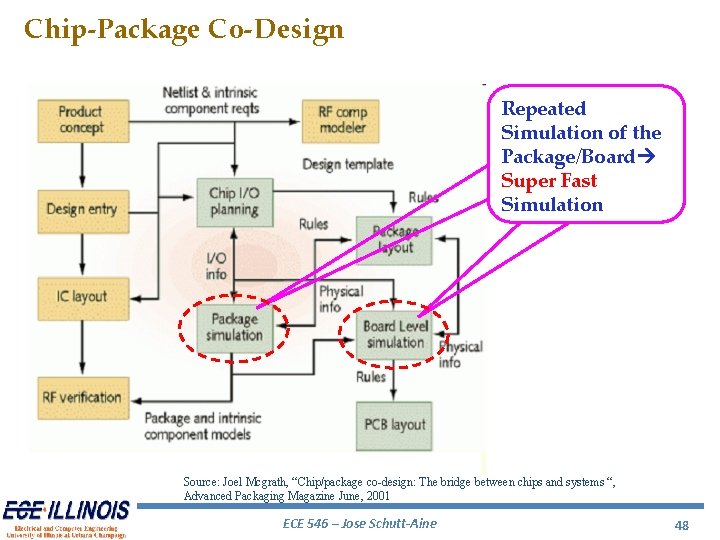
Chip-Package Co-Design Repeated Simulation of the Package/Board Super Fast Simulation Source: Joel Mcgrath, “Chip/package co-design: The bridge between chips and systems “, Advanced Packaging Magazine June, 2001 ECE 546 – Jose Schutt-Aine 48
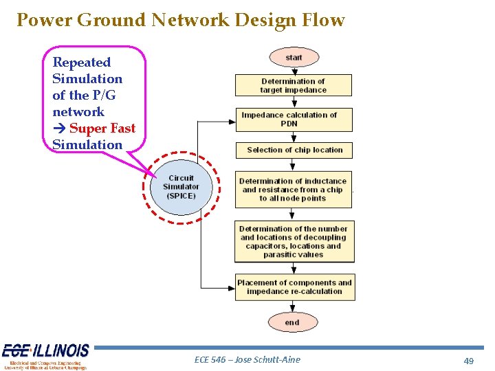
Power Ground Network Design Flow Repeated Simulation of the P/G network Super Fast Simulation ECE 546 – Jose Schutt-Aine 49
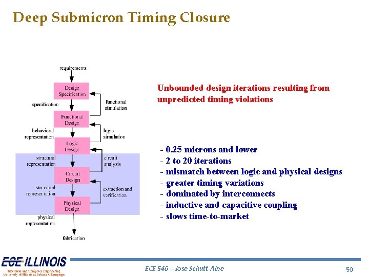
Deep Submicron Timing Closure Unbounded design iterations resulting from unpredicted timing violations - 0. 25 microns and lower - 2 to 20 iterations - mismatch between logic and physical designs - greater timing variations - dominated by interconnects - inductive and capacitive coupling - slows time-to-market ECE 546 – Jose Schutt-Aine 50
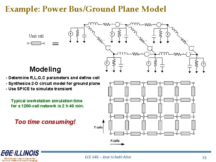
Example: Power Bus/Ground Plane Model Unit cell = Modeling - Determine R, L, G, C parameters and define cell - Synthesize 2 -D circuit model for ground plane - Use SPICE to simulate transient Typical workstation simulation time for a 1200 -cell network is 2 h 40 min. Too time consuming! ECE 546 – Jose Schutt-Aine 51
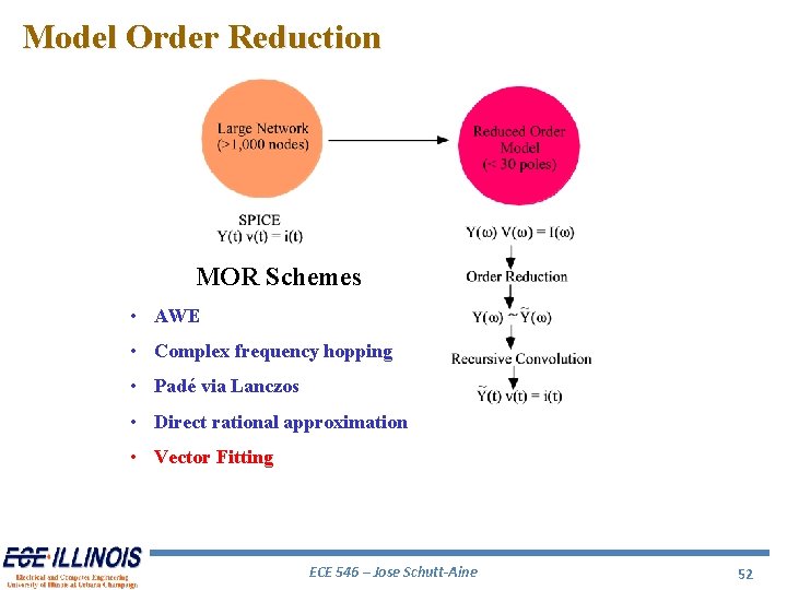
Model Order Reduction MOR Schemes • AWE • Complex frequency hopping • Padé via Lanczos • Direct rational approximation • Vector Fitting ECE 546 – Jose Schutt-Aine 52
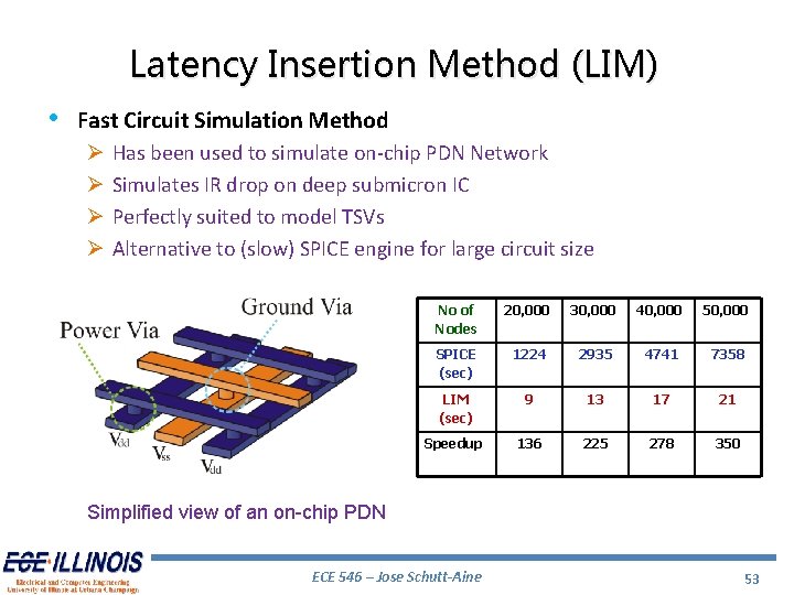
Latency Insertion Method (LIM) • Fast Circuit Simulation Method Ø Ø Has been used to simulate on-chip PDN Network Simulates IR drop on deep submicron IC Perfectly suited to model TSVs Alternative to (slow) SPICE engine for large circuit size No of Nodes 20, 000 30, 000 40, 000 50, 000 SPICE (sec) 1224 2935 4741 7358 LIM (sec) 9 13 17 21 Speedup 136 225 278 350 Simplified view of an on-chip PDN ECE 546 – Jose Schutt-Aine 53
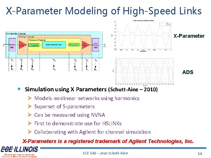
X-Parameter Modeling of High-Speed Links X-Parameter ADS • Simulation using X Parameters (Schutt-Aine – 2010) Ø Ø Ø Models nonlinear networks using harmonics Superset of S-parameters Can be measured using NVNA First to demonstrate use for HSLINKs Collaborating with Agilent for channel simulation X-Parameters is a registered trademark of Agilent Technologies, Inc. ECE 546 – Jose Schutt-Aine 54