ECE 448 Lecture 9 FPGA Design Flow George



- Slides: 30

ECE 448 Lecture 9 FPGA Design Flow George Mason University

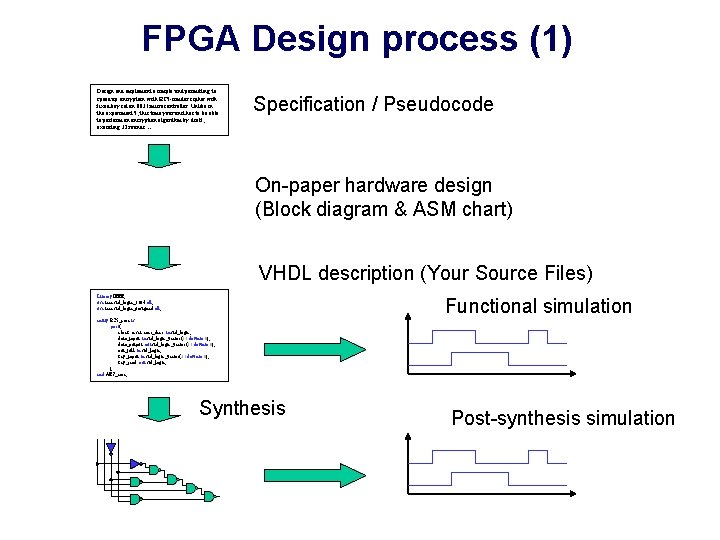
FPGA Design process (1) Design and implement a simple unit permitting to speed up encryption with RC 5 -similar cipher with fixed key set on 8031 microcontroller. Unlike in the experiment 5, this time your unit has to be able to perform an encryption algorithm by itself, executing 32 rounds…. . Specification / Pseudocode On-paper hardware design (Block diagram & ASM chart) VHDL description (Your Source Files) Library IEEE; use ieee. std_logic_1164. all; use ieee. std_logic_unsigned. all; Functional simulation entity RC 5_core is port( clock, reset, encr_decr: in std_logic; data_input: in std_logic_vector(31 downto 0); data_output: out std_logic_vector(31 downto 0); out_full: in std_logic; key_input: in std_logic_vector(31 downto 0); key_read: out std_logic; ); end AES_core; Synthesis Post-synthesis simulation

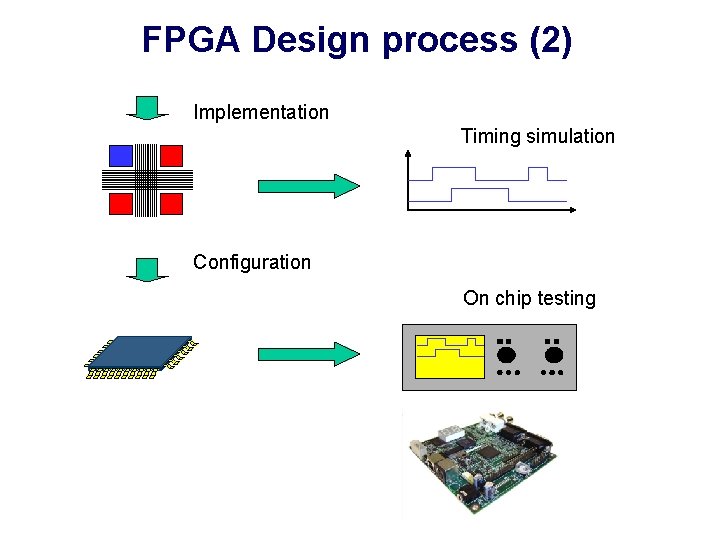
FPGA Design process (2) Implementation Timing simulation Configuration On chip testing

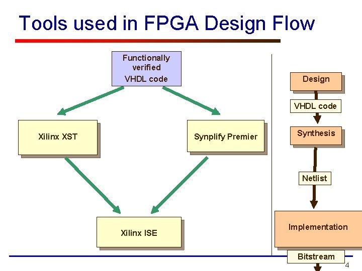
Tools used in FPGA Design Flow Functionally verified VHDL code Design VHDL code Xilinx XST Synplify Premier Synthesis Netlist Xilinx ISE Implementation Bitstream 4

Synthesis George Mason University

Synthesis Tools Xilinx XST Synplify Premier … and others 6

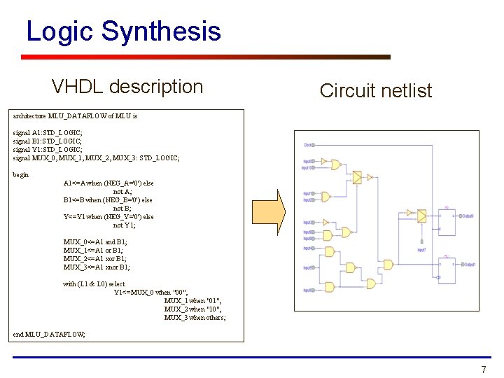
Logic Synthesis VHDL description Circuit netlist architecture MLU_DATAFLOW of MLU is signal A 1: STD_LOGIC; signal B 1: STD_LOGIC; signal Y 1: STD_LOGIC; signal MUX_0, MUX_1, MUX_2, MUX_3: STD_LOGIC; begin A 1<=A when (NEG_A='0') else not A; B 1<=B when (NEG_B='0') else not B; Y<=Y 1 when (NEG_Y='0') else not Y 1; MUX_0<=A 1 and B 1; MUX_1<=A 1 or B 1; MUX_2<=A 1 xor B 1; MUX_3<=A 1 xnor B 1; with (L 1 & L 0) select Y 1<=MUX_0 when "00", MUX_1 when "01", MUX_2 when "10", MUX_3 when others; end MLU_DATAFLOW; 7

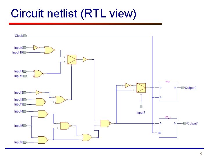
Circuit netlist (RTL view) 8

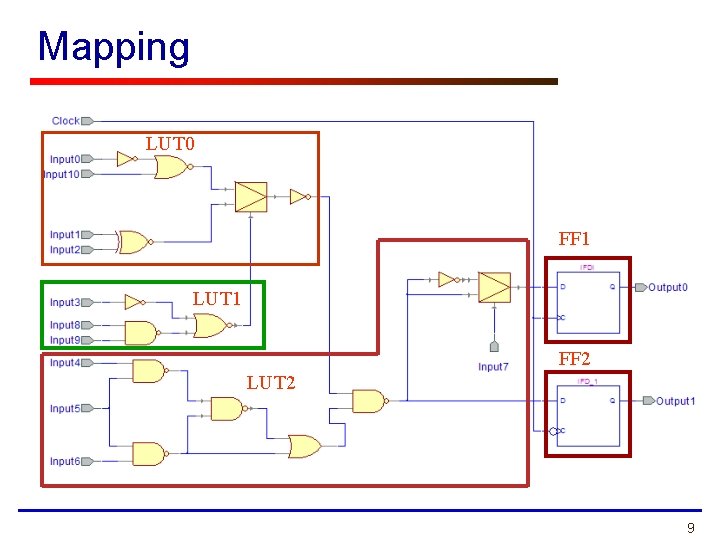
Mapping LUT 0 FF 1 LUT 1 FF 2 LUT 2 9

Implementation George Mason University

Implementation • After synthesis the entire implementation process is performed by FPGA vendor tools 11

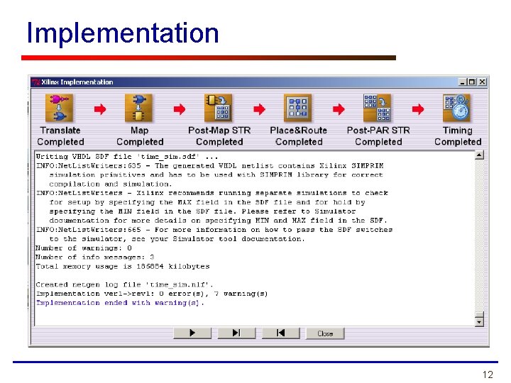
Implementation 12

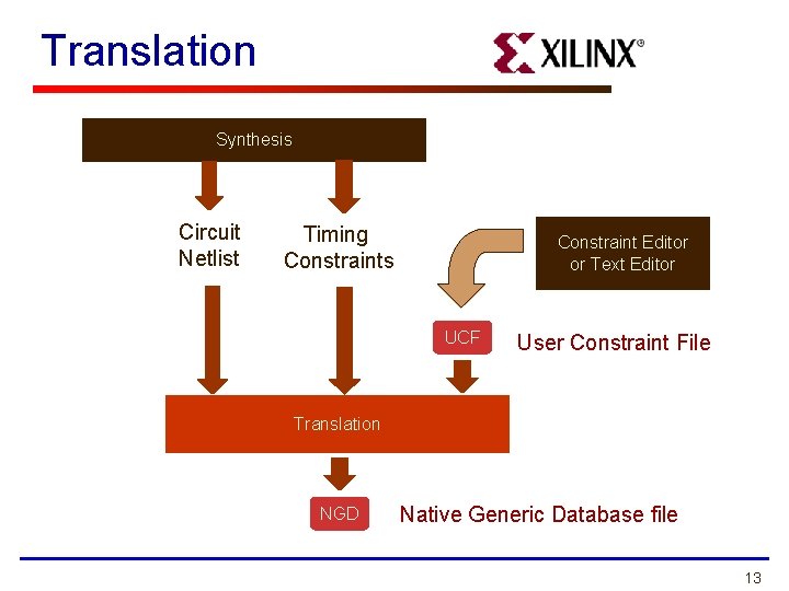
Translation Synthesis Circuit Netlist Timing Constraints Constraint Editor or Text Editor UCF User Constraint File Translation NGD Native Generic Database file 13

Mapping LUT 0 FF 1 LUT 1 FF 2 LUT 2 14

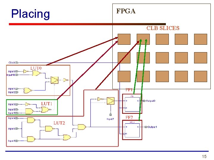
Placing FPGA CLB SLICES 15

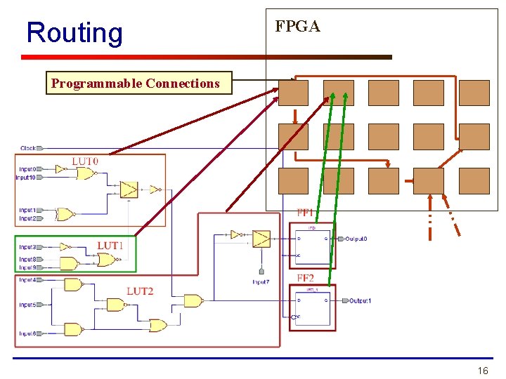
Routing FPGA Programmable Connections 16

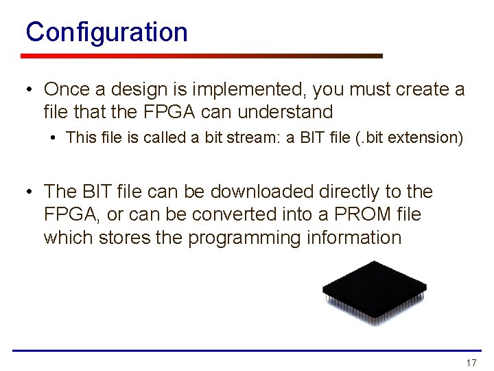
Configuration • Once a design is implemented, you must create a file that the FPGA can understand • This file is called a bit stream: a BIT file (. bit extension) • The BIT file can be downloaded directly to the FPGA, or can be converted into a PROM file which stores the programming information 17

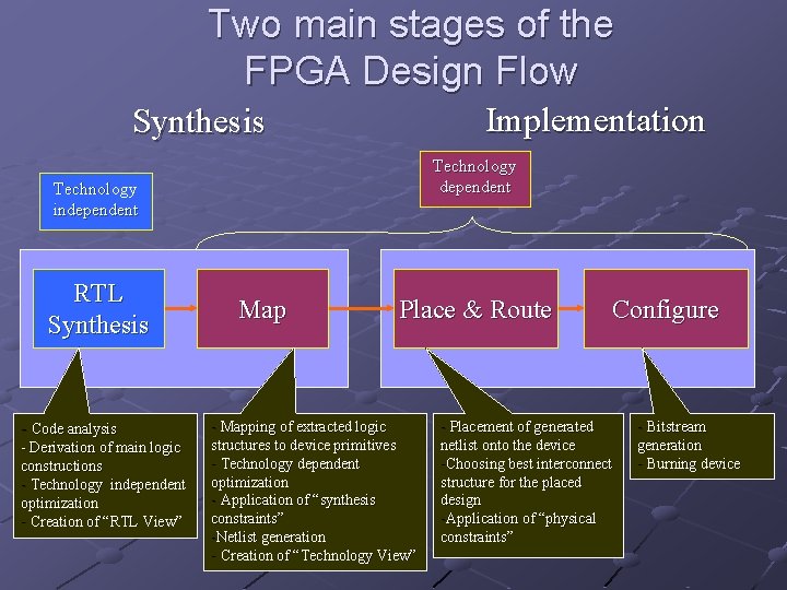
Two main stages of the FPGA Design Flow Implementation Synthesis Technology dependent Technology independent RTL Synthesis - Code analysis - Derivation of main logic constructions - Technology independent optimization - Creation of “RTL View” Map Place & Route - Mapping of extracted logic structures to device primitives - Technology dependent optimization - Application of “synthesis constraints” -Netlist generation - Creation of “Technology View” Configure - Placement of generated netlist onto the device -Choosing best interconnect structure for the placed design -Application of “physical constraints” - Bitstream generation - Burning device

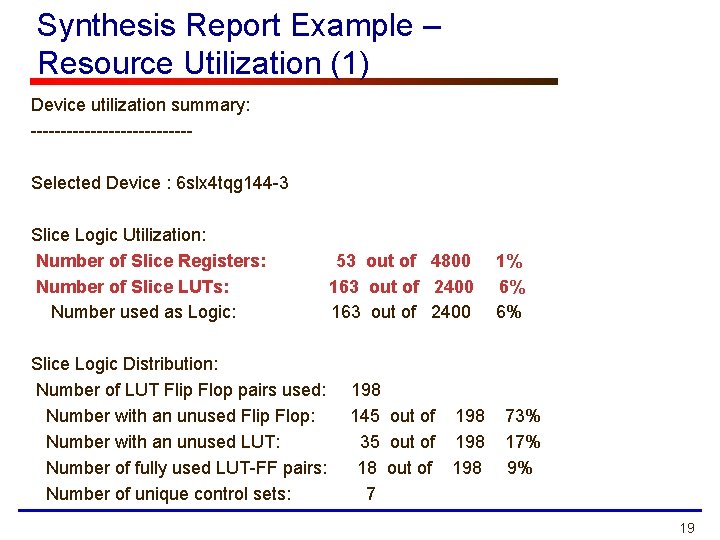
Synthesis Report Example – Resource Utilization (1) Device utilization summary: -------------Selected Device : 6 slx 4 tqg 144 -3 Slice Logic Utilization: Number of Slice Registers: Number of Slice LUTs: Number used as Logic: Slice Logic Distribution: Number of LUT Flip Flop pairs used: Number with an unused Flip Flop: Number with an unused LUT: Number of fully used LUT-FF pairs: Number of unique control sets: 53 out of 4800 163 out of 2400 198 145 out of 198 35 out of 198 18 out of 198 7 1% 6% 6% 73% 17% 9% 19

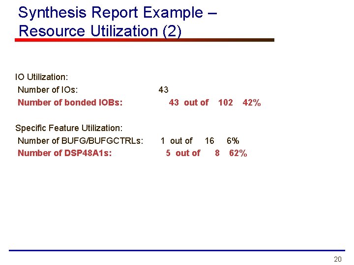
Synthesis Report Example – Resource Utilization (2) IO Utilization: Number of IOs: Number of bonded IOBs: Specific Feature Utilization: Number of BUFG/BUFGCTRLs: Number of DSP 48 A 1 s: 43 43 out of 102 42% 1 out of 16 6% 5 out of 8 62% 20

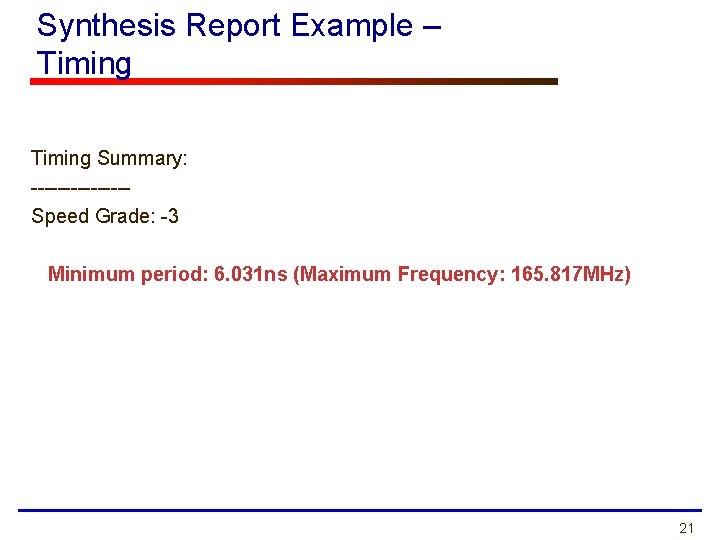
Synthesis Report Example – Timing Summary: -------Speed Grade: -3 Minimum period: 6. 031 ns (Maximum Frequency: 165. 817 MHz) 21

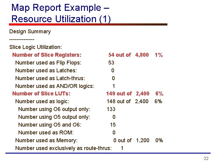
Map Report Example – Resource Utilization (1) Design Summary -------Slice Logic Utilization: Number of Slice Registers: 54 out of Number used as Flip Flops: 53 Number used as Latches: 0 Number used as Latch-thrus: 0 Number used as AND/OR logics: 1 Number of Slice LUTs: 149 out of Number used as logic: 148 out of Number using O 6 output only: 133 Number using O 5 output only: 0 Number using O 5 and O 6: 15 Number used as ROM: 0 Number used as Memory: 0 out of Number used exclusively as route-thrus: 1 4, 800 1% 2, 400 6% 1, 200 0% 22

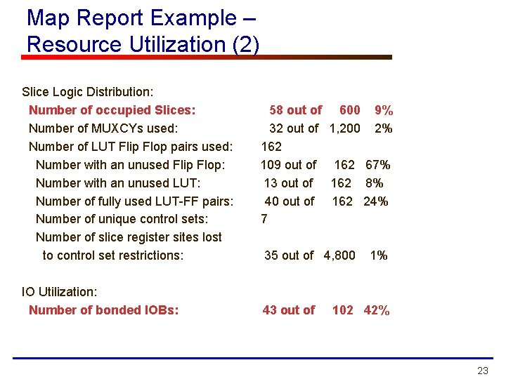
Map Report Example – Resource Utilization (2) Slice Logic Distribution: Number of occupied Slices: Number of MUXCYs used: Number of LUT Flip Flop pairs used: Number with an unused Flip Flop: Number with an unused LUT: Number of fully used LUT-FF pairs: Number of unique control sets: Number of slice register sites lost to control set restrictions: IO Utilization: Number of bonded IOBs: 58 out of 32 out of 162 109 out of 13 out of 40 out of 7 600 1, 200 162 67% 162 8% 162 24% 35 out of 4, 800 43 out of 9% 2% 1% 102 42% 23

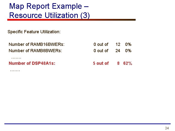
Map Report Example – Resource Utilization (3) Specific Feature Utilization: Number of RAMB 16 BWERs: Number of RAMB 8 BWERs: ……. Number of DSP 48 A 1 s: ……. 0 out of 5 out of 12 24 0% 0% 8 62% 24

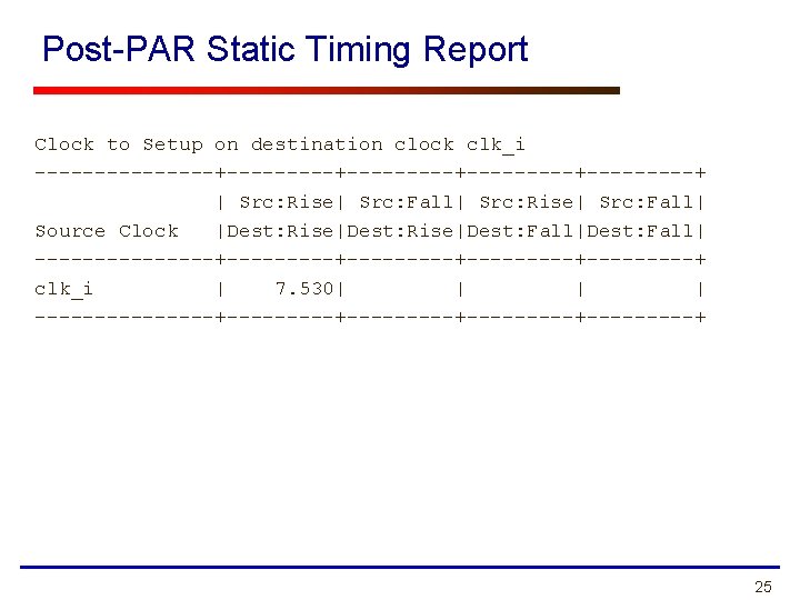
Post-PAR Static Timing Report Clock to Setup on destination clock clk_i --------+---------+---------+ | Src: Rise| Src: Fall| Source Clock |Dest: Rise|Dest: Fall| --------+---------+---------+ clk_i | 7. 530| | --------+---------+---------+ 25

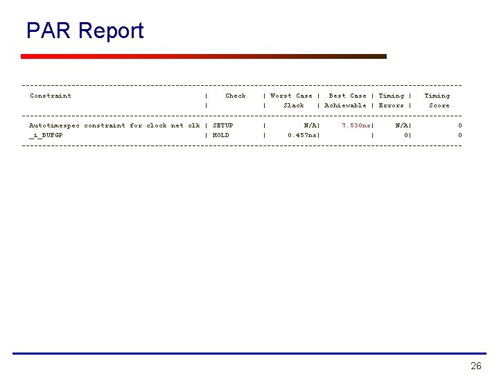
PAR Report -----------------------------------------------------Constraint | Check | Worst Case | Best Case | Timing | | Slack | Achievable | Errors | Score -----------------------------------------------------Autotimespec constraint for clock net clk | SETUP | N/A| 7. 530 ns| N/A| 0 _i_BUFGP | HOLD | 0. 457 ns| | 0| 0 ----------------------------------------------------- 26

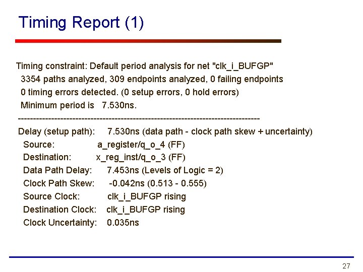
Timing Report (1) Timing constraint: Default period analysis for net "clk_i_BUFGP" 3354 paths analyzed, 309 endpoints analyzed, 0 failing endpoints 0 timing errors detected. (0 setup errors, 0 hold errors) Minimum period is 7. 530 ns. ----------------------------------------Delay (setup path): 7. 530 ns (data path - clock path skew + uncertainty) Source: a_register/q_o_4 (FF) Destination: x_reg_inst/q_o_3 (FF) Data Path Delay: 7. 453 ns (Levels of Logic = 2) Clock Path Skew: -0. 042 ns (0. 513 - 0. 555) Source Clock: clk_i_BUFGP rising Destination Clock: clk_i_BUFGP rising Clock Uncertainty: 0. 035 ns 27

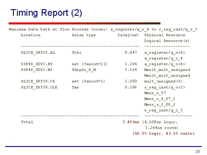
Timing Report (2) Maximum Data Path at Slow Process Corner: a_register/q_o_4 to x_reg_inst/q_o_3 Location Delay type Delay(ns) Physical Resource Logical Resource(s) -------------------------SLICE_X 4 Y 36. AQ Tcko 0. 447 a_register/q_o<4> a_register/q_o_4 DSP 48_X 0 Y 3. B 4 net (fanout=21) 1. 194 a_register/q_o<4> DSP 48_X 0 Y 3. M 3 Tdspdo_B_M 3. 364 Mmult_mult_unsigned SLICE_X 8 Y 39. C 4 net (fanout=1) 2. 050 mult_unsigned<3> SLICE_X 8 Y 39. CLK Tas 0. 398 x_reg_inst/q_o<3> Mmux_x_57 Mmux_x_4_f 7_2 Mmux_x_2_f 8_2 x_reg_inst/q_o_3 -------------------------Total 7. 453 ns (4. 209 ns logic, 3. 244 ns route) (56. 5% logic, 43. 5% route) 28

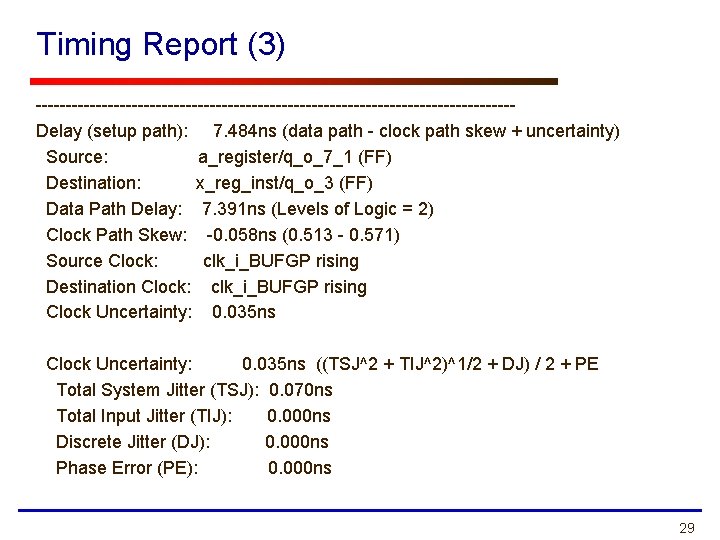
Timing Report (3) ----------------------------------------Delay (setup path): 7. 484 ns (data path - clock path skew + uncertainty) Source: a_register/q_o_7_1 (FF) Destination: x_reg_inst/q_o_3 (FF) Data Path Delay: 7. 391 ns (Levels of Logic = 2) Clock Path Skew: -0. 058 ns (0. 513 - 0. 571) Source Clock: clk_i_BUFGP rising Destination Clock: clk_i_BUFGP rising Clock Uncertainty: 0. 035 ns ((TSJ^2 + TIJ^2)^1/2 + DJ) / 2 + PE Total System Jitter (TSJ): 0. 070 ns Total Input Jitter (TIJ): 0. 000 ns Discrete Jitter (DJ): 0. 000 ns Phase Error (PE): 0. 000 ns 29

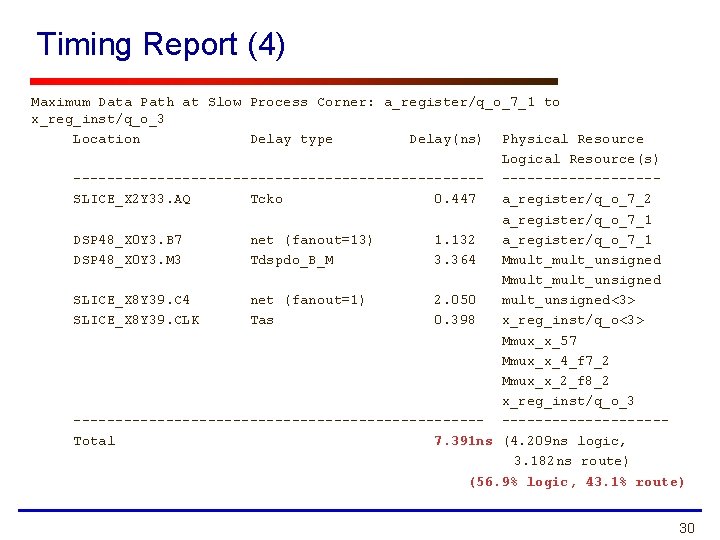
Timing Report (4) Maximum Data Path at Slow Process Corner: a_register/q_o_7_1 to x_reg_inst/q_o_3 Location Delay type Delay(ns) Physical Resource Logical Resource(s) -------------------------SLICE_X 2 Y 33. AQ Tcko 0. 447 a_register/q_o_7_2 a_register/q_o_7_1 DSP 48_X 0 Y 3. B 7 net (fanout=13) 1. 132 a_register/q_o_7_1 DSP 48_X 0 Y 3. M 3 Tdspdo_B_M 3. 364 Mmult_mult_unsigned SLICE_X 8 Y 39. C 4 net (fanout=1) 2. 050 mult_unsigned<3> SLICE_X 8 Y 39. CLK Tas 0. 398 x_reg_inst/q_o<3> Mmux_x_57 Mmux_x_4_f 7_2 Mmux_x_2_f 8_2 x_reg_inst/q_o_3 -------------------------Total 7. 391 ns (4. 209 ns logic, 3. 182 ns route) (56. 9% logic, 43. 1% route) 30