ECE 448 Lecture 12 FPro Video Subsystem VGA

ECE 448 Lecture 12 FPro Video Subsystem: VGA Frame Buffer Core ECE 448 – FPGA and ASIC Design with VHDL George Mason University

Required Reading • P. Chu, FPGA Prototyping by VHDL Examples Chapter 21. 1, Organization of the Video Subsystem Chapter 24, VGA Frame Buffer Core • Source Code of Examples http: //academic. csuohio. edu/chu_p/rtl/fpga_mcs_vhdl. html • Basys 3 FPGA Board Reference Manual 7. VGA Port ECE 448 – FPGA and ASIC Design with VHDL 2

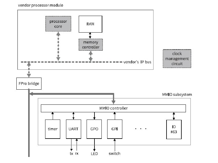
Top-level diagram of an FPro system
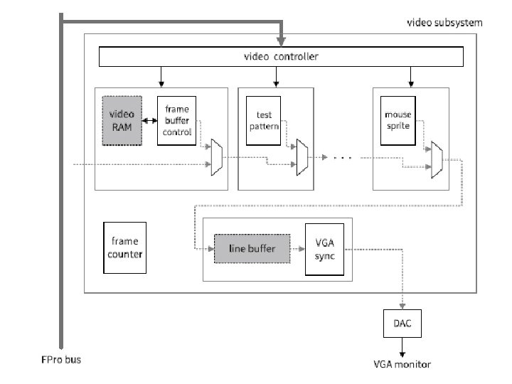

Video Subsystem • Establishes a framework to coordinate the operation of video cores. • A video core generates or processes the video data stream. • The cores are arranged as a cascading chain. • The data stream is pipelined and “blended” through each stage and eventually displayed on a VGA monitor. • The video subsystem demonstrates the principles of handling stream data, in which data are generated continuously and passed through a chain of components for processing.

Frame Buffer • A special memory module that hold the bitmap of a complete frame • Each pixel can be independently retrieved and updated • Read pipe: a data retrieving circuit that reads memory continuously at the pixel rate • Second port connected to the processor that generates or updates the content of the frame ECE 448 – FPGA and ASIC Design with VHDL 7

Frame Size • 640 x 480 VGA frame = 307. 2 K pixels 1 bit color: 307. 2 Kbit 3 bit color: 921. 6 Kbit 9 bit color: 2, 764. 8 Kbit 12 bit color: 3, 686. 4 Kbit = 38. 4 KByte = 115. 2 KByte = 345. 6 KByte = 460. 8 Kbyte On-chip memory of Artix-7 on Basys 3: 200 Kbyte On-chip memory of Artix-7 on Nexys 4: 540 Kbyte Memory of Micro. Blaze: 128 KByte ECE 448 – FPGA and ASIC Design with VHDL 8

Realization of 307. 2 K memory 256 K + 64 K = 320 K > 307. 2 K 256 K: 0 aa aaaa 64 K: 1 xx aaaa ECE 448 – FPGA and ASIC Design with VHDL 9
 library ieee; use ieee. std_logic_1164. all; use")
320 K x DW Memory Module (1) library ieee; use ieee. std_logic_1164. all; use ieee. numeric_std. all; entity vga_ram is generic( DW : integer : = 9 ); port( clk : in std_logic; we : in std_logic; addr_w : in std_logic_vector(18 downto 0); data_w : in std_logic_vector(DW - 1 downto 0); addr_r : in std_logic_vector(18 downto 0); data_r : out std_logic_vector(DW - 1 downto 0) ); end vga_ram; ECE 448 – FPGA and ASIC Design with VHDL 10
 architecture arch of vga_ram is signal data_r_256")
320 K x DW Memory Module (2) architecture arch of vga_ram is signal data_r_256 k : std_logic_vector(DW - 1 downto 0); signal data_r_64 k : std_logic_vector(DW - 1 downto 0); signal we_256 k : std_logic; signal we_64 k : std_logic; ECE 448 – FPGA and ASIC Design with VHDL 11
 begin -- instantiate 256 K RAM ram_256")
320 K x DW Memory Module (3) begin -- instantiate 256 K RAM ram_256 k_unit : entity work. sync_rw_port_ram(beh_arch) generic map( DATA_WIDTH => DW, ADDR_WIDTH => 18) port map( clk => clk, we => we_256 k, addr_w => addr_w(17 downto 0), din => data_w, addr_r => addr_r(17 downto 0), dout => data_r_256 k ); ECE 448 – FPGA and ASIC Design with VHDL 12
 -- instantiate 64 K RAM ram_64 k_unit")
320 K x DW Memory Module (4) -- instantiate 64 K RAM ram_64 k_unit : entity work. sync_rw_port_ram(beh_arch) generic map( DATA_WIDTH => DW, ADDR_WIDTH => 16) port map( clk => clk, we => we_64 k, addr_w => addr_w(15 downto 0), din => data_w, addr_r => addr_r(15 downto 0), dout => data_r_64 k ); ECE 448 – FPGA and ASIC Design with VHDL 13
 -- read data multiplexing data_r <= data_r_64")
320 K x DW Memory Module (5) -- read data multiplexing data_r <= data_r_64 k when addr_r(18) = '1' else data_r_256 k; -- write decoding we_256 k <= we and (not addr_w(18)); we_64 k <= we and addr_w(18); end arch; ECE 448 – FPGA and ASIC Design with VHDL 14
 addr = 640 * y + x addr")
Address Translation Pixel coordinates: (x, y) addr = 640 * y + x addr = 512 * y + 128 * y + x addr <= '0' & y(8 downto 0) & "00000") + + "000" & y(8 downto 0) & "0000000” + x; ECE 448 – FPGA and ASIC Design with VHDL 15
 library ieee; use ieee. std_logic_1164. all; use ieee.")
Frame Buffer Pixel Generation Circuit (1) library ieee; use ieee. std_logic_1164. all; use ieee. numeric_std. all; entity frame_src is generic( DW : integer : = 1 -- video RAM data width ); port( clk : std_logic; x, y : in std_logic_vector(10 downto 0); addr_pix : in std_logic_vector(18 downto 0); wr_data_pix : in std_logic_vector(DW - 1 downto 0); write_pix : in std_logic; frame_rgb : out std_logic_vector(DW - 1 downto 0) ); end frame_src; ECE 448 – FPGA and ASIC Design with VHDL 16
 architecture arch of frame_src is signal color :")
Frame Buffer Pixel Generation Circuit (2) architecture arch of frame_src is signal color : std_logic_vector(DW - 1 downto 0); signal y_offset : unsigned(18 downto 0); signal r_addr : std_logic_vector(18 downto 0); begin vram_unit : entity work. vga_ram generic map(DW => DW) port map( clk => clk, we => write_pix, addr_w => addr_pix(18 downto 0), data_w => wr_data_pix(DW - 1 downto 0), addr_r => r_addr, data_r => color ); ECE 448 – FPGA and ASIC Design with VHDL 17
 -- read address = 640*y + x =")
Frame Buffer Pixel Generation Circuit (3) -- read address = 640*y + x = 512*y + 128*y + x y_offset <= unsigned('0' & y(8 downto 0) & "00000") + unsigned("000" & y(8 downto 0) & "0000000"); r_addr <= std_logic_vector(y_offset + unsigned(x)); -- 1 clock delay line process(clk) begin if (clk'event and clk = '1') then frame_rgb <= color; end if; end process; end arch; ECE 448 – FPGA and ASIC Design with VHDL 18

Frame Buffer Memory: xaaa aaaa Bypass register: 1111 1111 ECE 448 – FPGA and ASIC Design with VHDL 19
 library ieee; use ieee. std_logic_1164. all; use ieee. numeric_std. all;")
Frame Buffer Core (1) library ieee; use ieee. std_logic_1164. all; use ieee. numeric_std. all; entity chu_frame_buffer_core is generic( DW : integer : = 9 -- frame buffer RAM data width ); ECE 448 – FPGA and ASIC Design with VHDL 20
 port( clk : in std_logic; reset : in std_logic; x")
Frame Buffer Core (2) port( clk : in std_logic; reset : in std_logic; x : in std_logic_vector(10 downto 0); y : in std_logic_vector(10 downto 0); -- video interface cs : in std_logic; write : in std_logic; addr : in std_logic_vector(19 downto 0); wr_data : in std_logic_vector(31 downto 0); -- stream interface si_rgb : in std_logic_vector(DW - 1 downto 0); so_rgb : out std_logic_vector(DW - 1 downto 0) ); end chu_frame_buffer_core; ECE 448 – FPGA and ASIC Design with VHDL 21
 architecture arch of chu_frame_buffer_core is signal wr_pix : std_logic; signal")
Frame Buffer Core (3) architecture arch of chu_frame_buffer_core is signal wr_pix : std_logic; signal wr_en : std_logic; signal wr_bypass : std_logic; signal bypass_reg : std_logic; signal frame_rgb : std_logic_vector(DW - 1 downto 0); ECE 448 – FPGA and ASIC Design with VHDL 22
 -- instantiate pixel generation circuit frame_gen_unit : entity work. frame_src")
Frame Buffer Core (4) -- instantiate pixel generation circuit frame_gen_unit : entity work. frame_src generic map( CD => CD, DW => DW ) port map( clk => clk, x => x, y => y, addr_pix => addr(18 downto 0), wr_data_pix => wr_data(DW - 1 downto 0), write_pix => wr_pix, frame_rgb => frame_rgb ); ECE 448 – FPGA and ASIC Design with VHDL 23
 -- register process(clk, reset) begin if reset = '1' then")
Frame Buffer Core (5) -- register process(clk, reset) begin if reset = '1' then bypass_reg <= '0'; elsif (clk'event and clk = '1') then if wr_bypass = '1' then bypass_reg <= wr_data(0); end if; end process; ECE 448 – FPGA and ASIC Design with VHDL 24
 -- decoding logic wr_en <= '1' when write = '1'")
Frame Buffer Core (6) -- decoding logic wr_en <= '1' when write = '1' and cs = '1' else '0'; wr_bypass <= '1' when addr = x"fffff" and wr_en = '1' else '0'; wr_pix <= '1' when addr /= x"fffff" and wr_en = '1' else '0'; -- stream blending: mux so_rgb <= si_rgb when bypass_reg = '1' else frame_rgb; end arch; ECE 448 – FPGA and ASIC Design with VHDL 25
 (1) class Frame. Core { public: enum {")
Frame Core Class Definition (vga_core. h) (1) class Frame. Core { public: enum { BYPASS_REG = 0 x 7 ffff /**< bypass control register */ }; enum { HMAX = 640, /**< 640 pixels per row */ VMAX = 480 /**< 480 pixels per row */ }; /* methods */ Frame. Core(uint 32_t frame_base_addr); ~Frame. Core(); ECE 448 – FPGA and ASIC Design with VHDL 26
 (2) /** * write a pxiel to frame")
Frame Core Class Definition (vga_core. h) (2) /** * write a pxiel to frame buffer * @param x x-coordinate of the pxixel (between 0 and HMAX) * @param y y-coordinate of the pxixel (between 0 and VMAX) * @param color pixel color * */ void wr_pix(int x, int y, int color); /** * clear frame buffer (fill the frame with a specific color) * @param color to fill the frame * */ void clr_screen(int color); ECE 448 – FPGA and ASIC Design with VHDL 27
 (3) /** * generate pixels for a line")
Frame Core Class Definition (vga_core. h) (3) /** * generate pixels for a line in frame buffer (plot a line) * @param x 1 x-coordinate of starting point * @param y 1 y-coordinate of starting point * @param x 2 x-coordinate of ending point * @param y 2 y-coordinate of ending point * @param color line color * */ void plot_line(int x 1, int y 1, int x 2, int y 2, int color); /** * enable/disable core bypass * @param by 1: bypass current core; 0: not bypass * */ void bypass(int by); ECE 448 – FPGA and ASIC Design with VHDL 28
 (4) private: uint 32_t base_addr; void swap(int &a,")
Frame Core Class Definition (vga_core. h) (4) private: uint 32_t base_addr; void swap(int &a, int &b); }; ECE 448 – FPGA and ASIC Design with VHDL 29
- Slides: 29