ECE 448 Lab 3 Part 2 Design of
ECE 448 Lab 3 – Part 2 Design of Controllers Using ASM Charts
Agenda for Today Part 1: Post-synthesis and Timing Simulation using Vivado Simulator Part 2: Discussion of Solutions to Lab 3 Exercise 1 Part 3: Introduction to Lab 3 Exercise 2 Part 4: Q&A for Lab Assignment 2
Part 1 Hands-on Session on Post-synthesis and Timing Simulation Using Vivado Simulator

Part 2 Discussion of Solutions to Class Exercise 1
Part 3 Introduction to Class Exercise 2
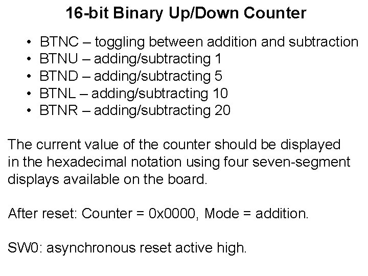
16 -bit Binary Up/Down Counter • • • BTNC – toggling between addition and subtraction BTNU – adding/subtracting 1 BTND – adding/subtracting 5 BTNL – adding/subtracting 10 BTNR – adding/subtracting 20 The current value of the counter should be displayed in the hexadecimal notation using four seven-segment displays available on the board. After reset: Counter = 0 x 0000, Mode = addition. SW 0: asynchronous reset active high.
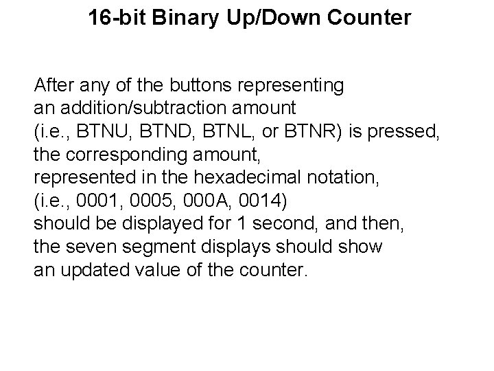
16 -bit Binary Up/Down Counter After any of the buttons representing an addition/subtraction amount (i. e. , BTNU, BTND, BTNL, or BTNR) is pressed, the corresponding amount, represented in the hexadecimal notation, (i. e. , 0001, 0005, 000 A, 0014) should be displayed for 1 second, and then, the seven segment displays should show an updated value of the counter.
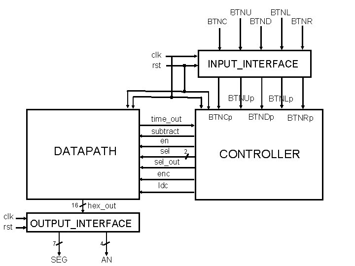
BTNU BTNL BTNC BTNS BTND BTNR clk rst INPUT_INTERFACE BTNUp BTNCp BTNSp time_out DATAPATH 16 clk rst hex_out OUTPUT_INTERFACE 7 4 SEG AN subtract en sel_out enc ldc 2 BTNLp BTNDp BTNRp CONTROLLER
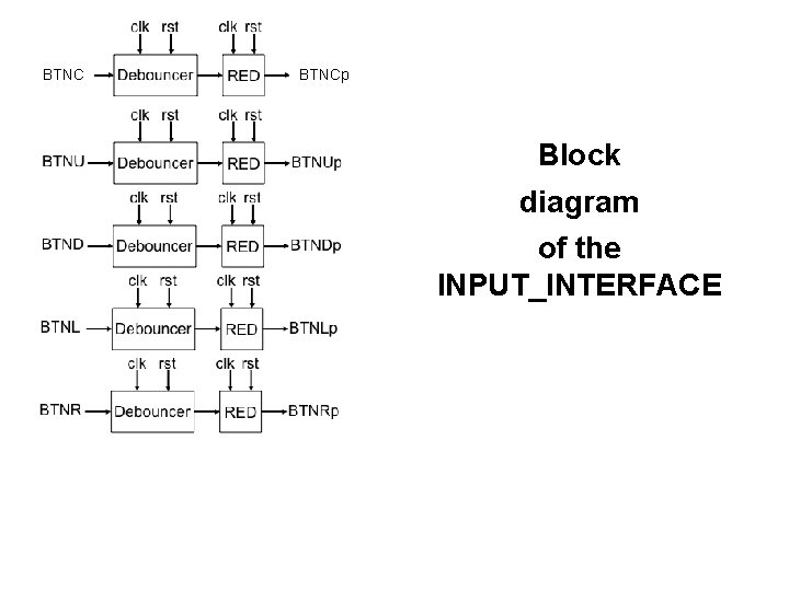
BTNCp Block diagram of the INPUT_INTERFACE
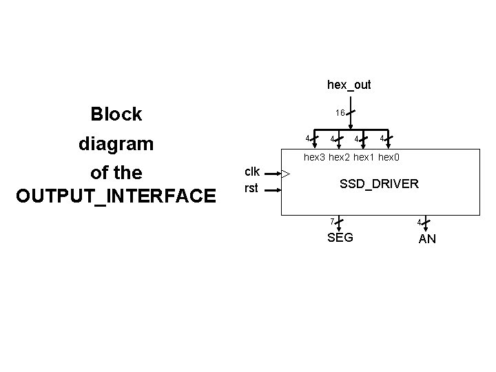
hex_out Block 16 diagram of the OUTPUT_INTERFACE 4 4 hex 3 hex 2 hex 1 hex 0 clk rst SSD_DRIVER 7 SEG 4 AN
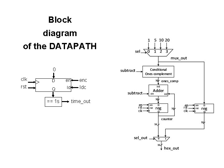
Block diagram of the DATAPATH 0 clk rst D en Q ld == 1 s enc ldc time_out rst clk
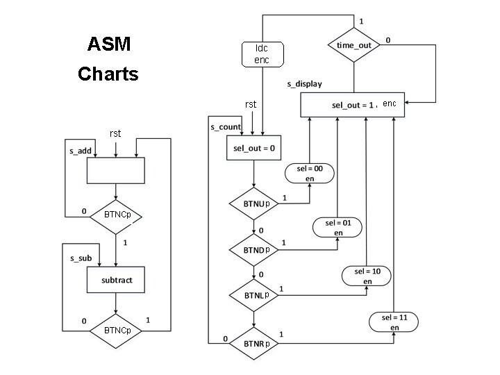
ASM Charts ldc enc rst , enc rst p BTNCp p p
Tasks 1. Describe the circuit in synthesizable VHDL. 2. Develop a testbench with two versions of timing constants, one used for simulation, and the other used for the actual operation of the circuit on the board. 3. Perform functional simulation of your code using the Vivado Simulator. 4. Synthesize your code using Xilinx Vivado. 5. Prepare the correct XDC (Xilinx Design Constraints) file. 6. Implement your circuit using Xilinx Vivado. 7. Check thoroughly all implementation reports. Pay attention to timing, resource utilization, and pin allocations. 8. Perform post-synthesis and timing simulations of your circuit using the Vivado Simulator. 9. Check very carefully your pin allocations listed in the report files. Download your bitstream to the FPGA board. 10. Test the operation of your circuit experimentally using the Basys 3 FPGA Board.
Deliverables 1. Synthesizable VHDL code. 2. Testbench. 3. XDC file. 4. Resource utilization reported by Vivado. 5. A short video demonstrating the required functionality realized using Basys 3 (if a fully working design was not demonstrated to the TA during the lab session when this exercise was introduced). 6. Timing waveforms obtained from timing simulation, demonstrating what happens in the circuit 10 cycles before and 10 cycles after BTNRp is set to 1 (stored as PDF files).
- Slides: 14