ECE 448 Lab 2 Implementing Combinational and Sequential

ECE 448 Lab 2 Implementing Combinational and Sequential Logic in VHDL ECE 448 – FPGA and ASIC Design with VHDL George Mason University
Agenda for today Part 1: Introduction to Lab 2 Implementing Combinational and Sequential Logic in VHDL Part 2: Hands-on Session: Simulation Using Aldec Active-HDL Part 3: Lab Exercise 1 2
Part 1 Introduction to Lab 2 ECE 448 – FPGA and ASIC Design with VHDL

Discussion of the Diagram, Requirements, and Hints
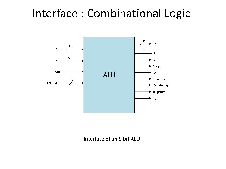
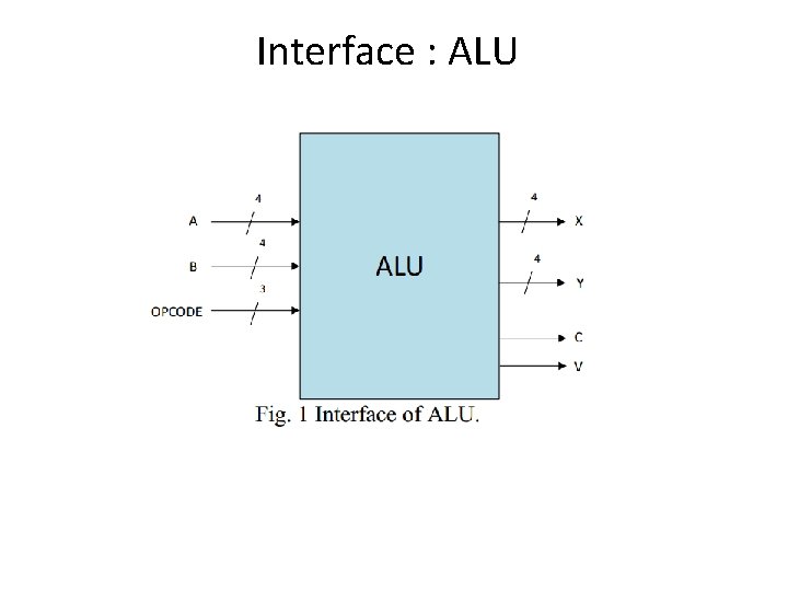
Interface : Combinational Logic Interface of an 8 -bit ALU
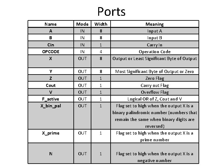
Ports Name A B Cin OPCODE X Mode IN IN OUT Width 8 8 1 4 8 Meaning Input A Input B Carry In Operation Code Output or Least Significant Byte of Output Y Z Cout V F_active X_bin_pal OUT OUT OUT 8 1 1 1 X_prime OUT 1 Most Significant Byte of Output or Zero Flag Carry out Flag Overflow Flag Logical OR of Z, Cout and V Flag set to high when the output X is a binary palindromic number (numbers that remain the same when binary digits are reversed) Flag set to high when the output X is a prime number N OUT 1 Flag set to high when the output X is a negative number
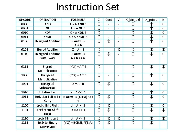
Instruction Set OPCODE 0000 0001 0010 0011 0100 OPERATION AND OR XNOR Unsigned Addition 0101 0110 Signed Addition Unsigned Addition with Carry 0111 Signed (Y: X) = A * B Multiplication Unsigned X = A - B Subtraction Rotation Left X = A <<< 1 Rotation Left with (Cout: X) = (Cin: A) <<< Carry 1 Logic Shift Right X = A >> 1 Arithmetic Shift X = A >> 1 Right Logic Shift Left X = A << 1 BCD to Binary (Y: X) = BCD 2 BIN(B: A) Conversion 1000 1001 1010 1011 1100 1101 1110 1111 FORMULA X = A AND B X = A OR B X = A XNOR B (Cout: X) = A + B X = A + B (Cout: X) = A + B + Cin Z ↕ ↕ ↕ Cout ↕ V X_bin_pal ↕ ↕ ↕ X_prime ↕ ↕ ↕ N 0 0 0 ↕ ↕ ↕ 0 ↕ ↕ ↕ 0 ↕ ↕ ↕ ↕ ↕ 0 0 ↕ ↕ ↕ ↕ 0 ↕ ↕ ↕
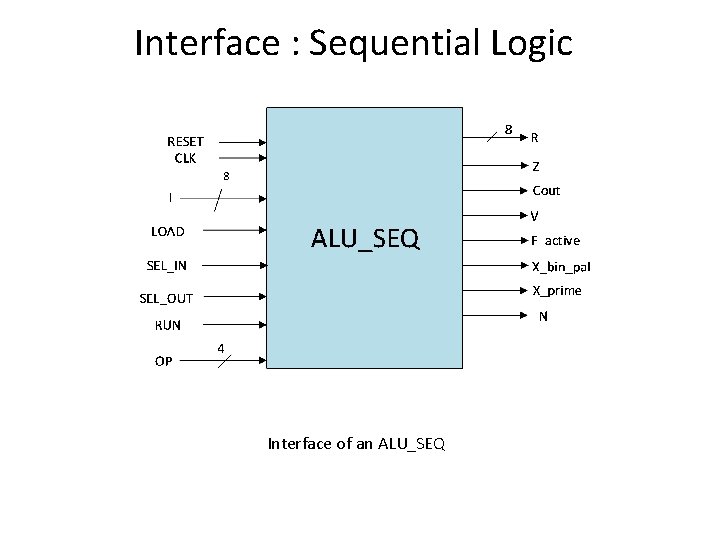
Interface : Sequential Logic Interface of an ALU_SEQ
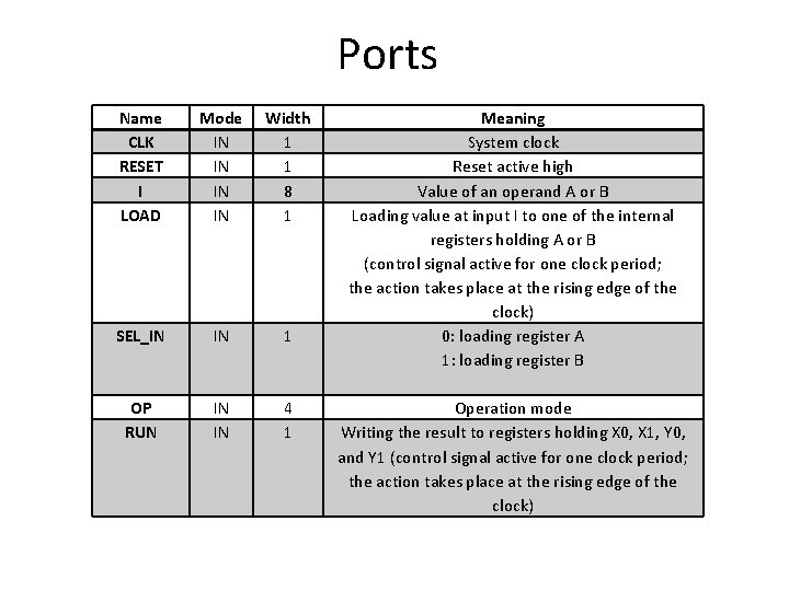
Ports Name CLK RESET I LOAD Mode IN IN Width 1 1 8 1 SEL_IN IN 1 Meaning System clock Reset active high Value of an operand A or B Loading value at input I to one of the internal registers holding A or B (control signal active for one clock period; the action takes place at the rising edge of the clock) 0: loading register A 1: loading register B OP RUN IN IN 4 1 Operation mode Writing the result to registers holding X 0, X 1, Y 0, and Y 1 (control signal active for one clock period; the action takes place at the rising edge of the clock)
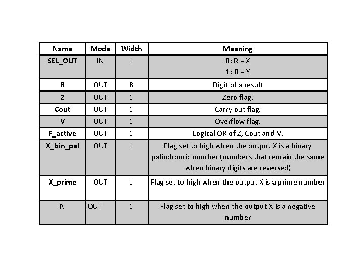
Name SEL_OUT Mode IN Width 1 Meaning 0: R = X 1: R = Y R Z Cout V OUT OUT 8 1 1 1 Digit of a result Zero flag. Carry out flag. Overflow flag. F_active X_bin_pal OUT 1 1 Logical OR of Z, Cout and V. Flag set to high when the output X is a binary palindromic number (numbers that remain the same when binary digits are reversed) X_prime OUT 1 Flag set to high when the output X is a prime number 1 Flag set to high when the output X is a negative number N OUT
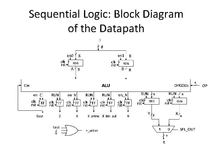
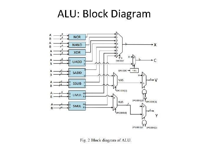
Sequential Logic: Block Diagram of the Datapath
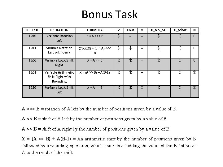
Bonus Task OPCODE OPERATION FORMULA Z Cout V X_bin_pal X_prime N 1010 Variable Rotation Left X = A <<< B ↕ ↕ ↕ 0 1011 Variable Rotation Left with Carry (Cout: X) = (Cin: A) <<< B ↕ ↕ 0 1100 Variable Logic Shift Right X = A >> B ↕ ↕ 0 1101 Variable Arithmetic Shift Right with Rounding X = (A >> B) + A(B-1) ↕ ↕ ↕ 1110 Variable Logic Shift Left X = A << B ↕ ↕ ↕ A <<< B = rotation of A left by the number of positions given by a value of B. A << B = shift of A left by the number of positions given by a value of B. A >> B = shift of A right by the number of positions given by a value of B. X = (A >> B) + A(B-1) = An arithmetic shift by the number of positions given by B followed by a rounding operation, which consists of adding the value of the B-1 st bit of A to the result of the shift.
Part 2 Hands-on Session: Simulation Using Aldec Active-HDL ECE 448 – FPGA and ASIC Design with VHDL

Hands-on Session based on the MLU example with simple testbench
Part 3 Lab Exercise 1 ECE 448 – FPGA and ASIC Design with VHDL
Interface : ALU
ALU: Block Diagram
- Slides: 17