ECE 434 Advanced Digital System L 04 Electrical
- Slides: 27

ECE 434 Advanced Digital System L 04 Electrical and Computer Engineering University of Western Ontario UAH-CPE/EE 422/522 AM

Outline • What we know – Combinational Networks • Analysis • Synthesis AND-OR-NOTs, NORs, NANDs, MUXes, ROMs, PLAs • Hazards in combinational networks • What we do not know – PALs – Sequential Networks • Basic Building Blocks • Mealy Sequential Networks 12/20/2021 UAH-CPE/EE 422/522 AM 2

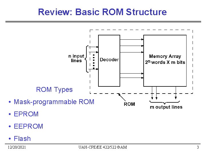
Review: Basic ROM Structure ROM Types • Mask-programmable ROM • EPROM • EEPROM • Flash 12/20/2021 UAH-CPE/EE 422/522 AM 3

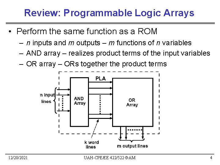
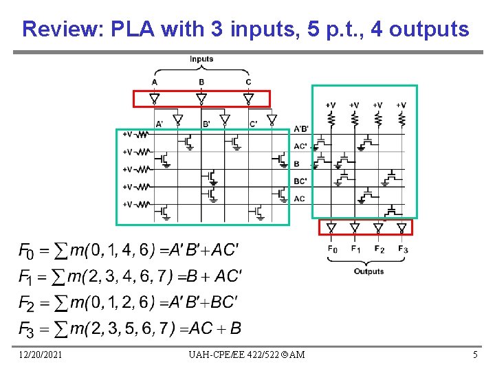
Review: Programmable Logic Arrays • Perform the same function as a ROM – n inputs and m outputs – m functions of n variables – AND array – realizes product terms of the input variables – OR array – ORs together the product terms 12/20/2021 UAH-CPE/EE 422/522 AM 4

Review: PLA with 3 inputs, 5 p. t. , 4 outputs 12/20/2021 UAH-CPE/EE 422/522 AM 5

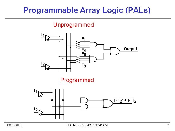
Programmable Array Logic (PALs) • PLAs – Both AND and OR arrays are programmable • PAL is a special case of PLA – AND array is programmable and OR array is fixed • Motivation for PALs – Programmable switches historically presented two difficulties to the manufacturers • hard to fabricate correctly => increase the price • reduce the speed performance of circuits – PALs are less expensive, faster, and easier to program • Disadvantage: less flexible 12/20/2021 UAH-CPE/EE 422/522 AM 6

Programmable Array Logic (PALs) Unprogrammed Programmed 12/20/2021 UAH-CPE/EE 422/522 AM 7

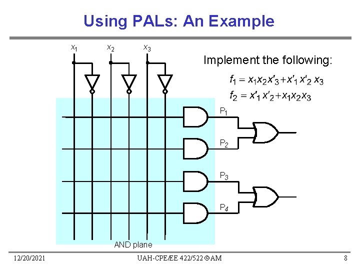
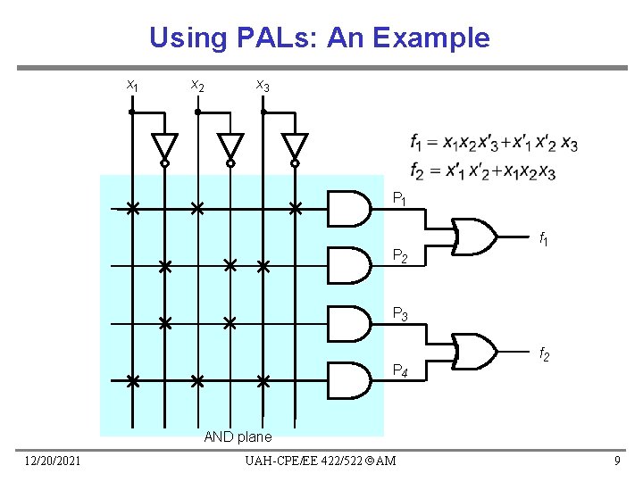
Using PALs: An Example x 1 x 2 x 3 Implement the following: P 1 P 2 P 3 P 4 AND plane 12/20/2021 UAH-CPE/EE 422/522 AM 8

Using PALs: An Example x 1 x 2 x 3 P 1 P 2 f 1 P 3 P 4 f 2 AND plane 12/20/2021 UAH-CPE/EE 422/522 AM 9

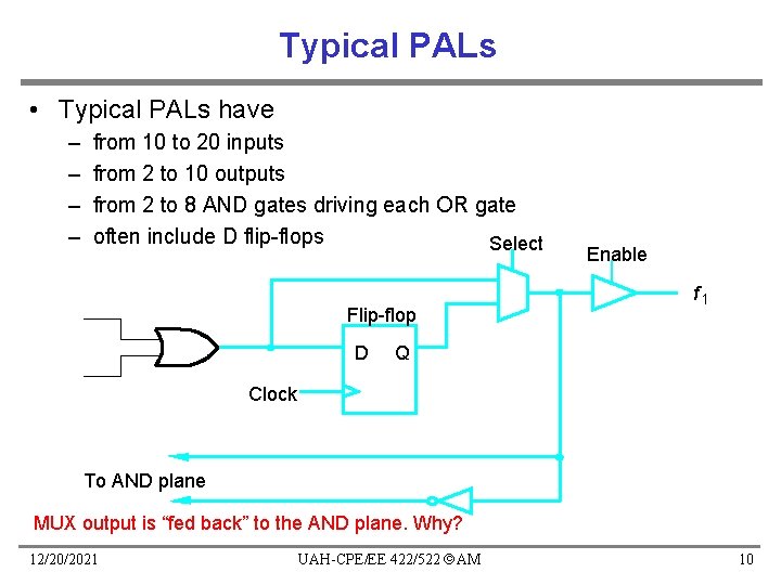
Typical PALs • Typical PALs have – – from 10 to 20 inputs from 2 to 10 outputs from 2 to 8 AND gates driving each OR gate often include D flip-flops Select Flip-flop D Enable f 1 Q Clock To AND plane MUX output is “fed back” to the AND plane. Why? 12/20/2021 UAH-CPE/EE 422/522 AM 10

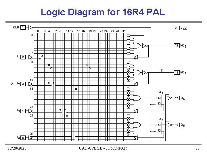
Logic Diagram for 16 R 4 PAL 12/20/2021 UAH-CPE/EE 422/522 AM 11

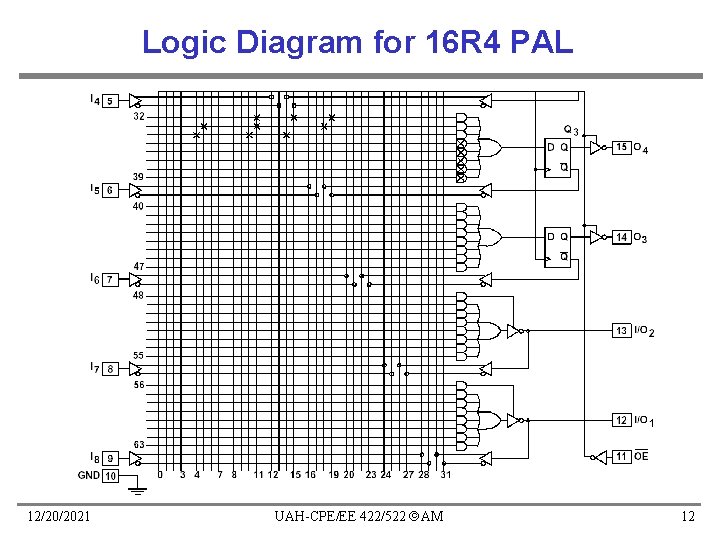
Logic Diagram for 16 R 4 PAL 12/20/2021 UAH-CPE/EE 422/522 AM 12

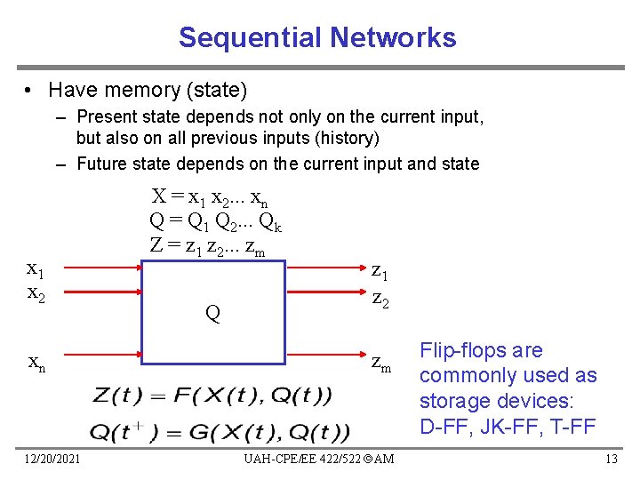
Sequential Networks • Have memory (state) – Present state depends not only on the current input, but also on all previous inputs (history) – Future state depends on the current input and state x 1 x 2 xn 12/20/2021 X = x 1 x 2. . . xn Q = Q 1 Q 2. . . Qk Z = z 1 z 2. . . zm Q z 1 z 2 zm UAH-CPE/EE 422/522 AM Flip-flops are commonly used as storage devices: D-FF, JK-FF, T-FF 13

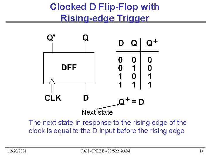
Clocked D Flip-Flop with Rising-edge Trigger Next state The next state in response to the rising edge of the clock is equal to the D input before the rising edge 12/20/2021 UAH-CPE/EE 422/522 AM 14

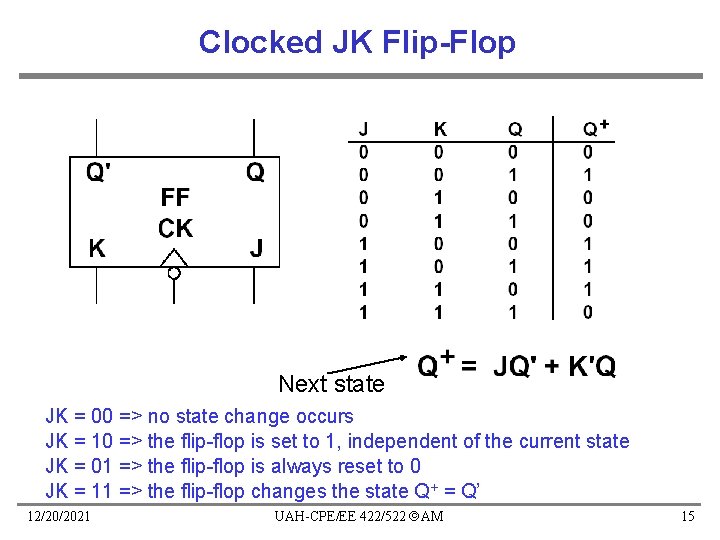
Clocked JK Flip-Flop Next state JK = 00 => no state change occurs JK = 10 => the flip-flop is set to 1, independent of the current state JK = 01 => the flip-flop is always reset to 0 JK = 11 => the flip-flop changes the state Q+ = Q’ 12/20/2021 UAH-CPE/EE 422/522 AM 15

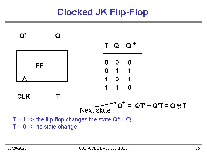
Clocked JK Flip-Flop Next state T = 1 => the flip-flop changes the state Q+ = Q’ T = 0 => no state change 12/20/2021 UAH-CPE/EE 422/522 AM 16

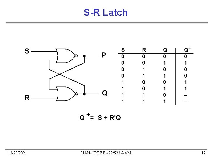
S-R Latch 12/20/2021 UAH-CPE/EE 422/522 AM 17

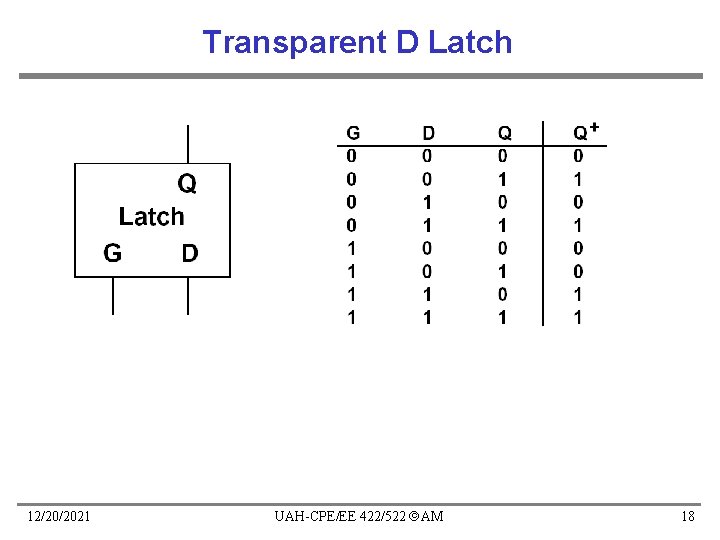
Transparent D Latch 12/20/2021 UAH-CPE/EE 422/522 AM 18

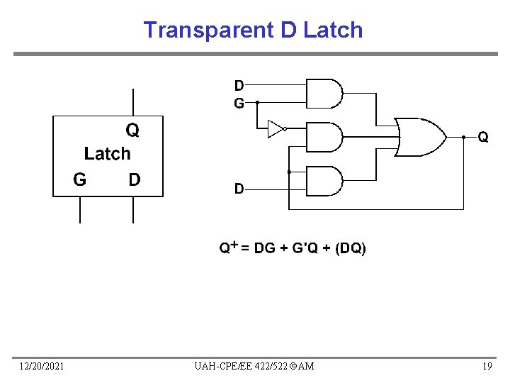
Transparent D Latch 12/20/2021 UAH-CPE/EE 422/522 AM 19

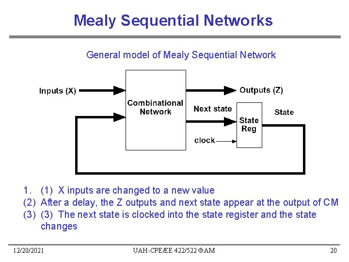
Mealy Sequential Networks General model of Mealy Sequential Network 1. (1) X inputs are changed to a new value (2) After a delay, the Z outputs and next state appear at the output of CM (3) The next state is clocked into the state register and the state changes 12/20/2021 UAH-CPE/EE 422/522 AM 20

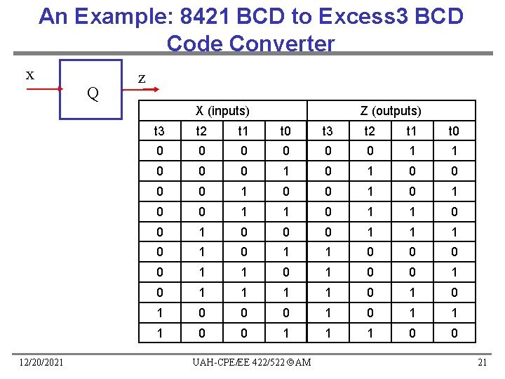
An Example: 8421 BCD to Excess 3 BCD Code Converter x Q z X (inputs) 12/20/2021 Z (outputs) t 3 t 2 t 1 t 0 0 0 0 1 1 0 0 0 1 0 0 1 1 0 0 0 1 1 1 0 0 1 1 0 0 1 1 1 1 0 1 0 0 0 1 1 1 0 0 UAH-CPE/EE 422/522 AM 21

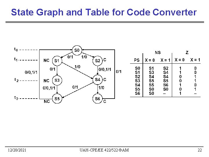
State Graph and Table for Code Converter 12/20/2021 UAH-CPE/EE 422/522 AM 22

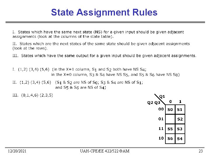
State Assignment Rules 12/20/2021 UAH-CPE/EE 422/522 AM 23

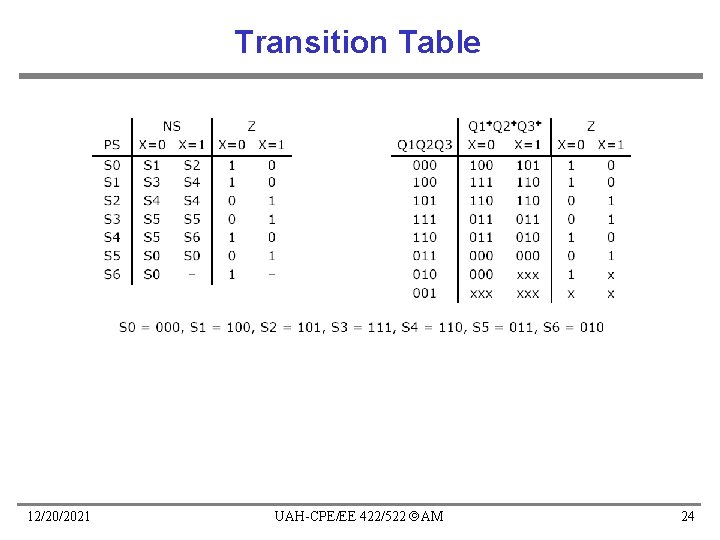
Transition Table 12/20/2021 UAH-CPE/EE 422/522 AM 24

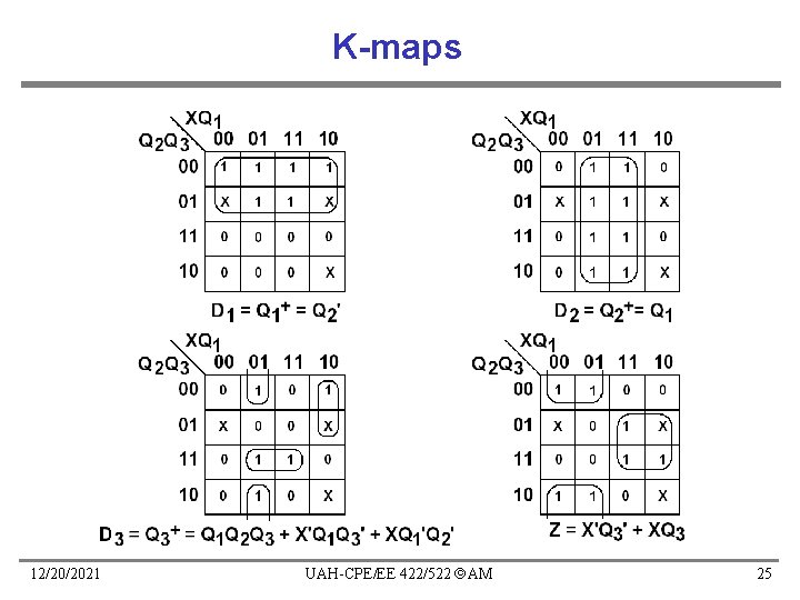
K-maps 12/20/2021 UAH-CPE/EE 422/522 AM 25

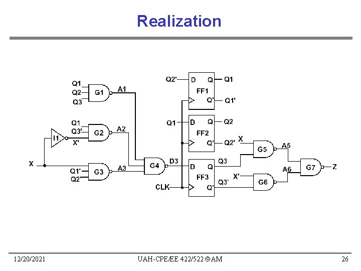
Realization 12/20/2021 UAH-CPE/EE 422/522 AM 26

To Do • Study textbook chapters – 3. 1, 3. 2, 3. 3, 1. 6, 1. 7 • Do homework #1 12/20/2021 UAH-CPE/EE 422/522 AM 27