ECE 426 VLSI System Design Lecture 12 Timing




- Slides: 29

ECE 426 - VLSI System Design Lecture 12 - Timing, Project Overview Prof. John Nestor ECE Department Lafayette College Easton, Pennsylvania 18042 nestorj@lafayette. edu 3/10/03 Lecture 12 - Timing, Proj. Overview 1

Announcements } Exam 1 - Take-Home } Out: March 24 } Due: March 31 } Timing References } Synopys Online Documentation (SOLD) Manuals access using the "sold" command: • Design Compiler User Guide • Design Compiler Tutorial • Design Compiler Reference Manual } Pran Kurup and Taher Abbasi, Logic Synthesis using Sysnopsys®, 2 nd ed. , Kluwer Academic Publishers, 1997. 3/10/03 Lecture 12 - Timing, Proj. Overview 2

Where we are. . . } Last Time } State Coding & Assignment } Timing } Today } Timing in Synopsys Tools } Project Overview 3/10/03 Lecture 12 - Timing, Proj. Overview 3

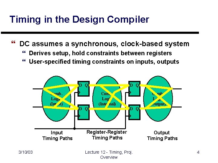
Timing in the Design Compiler } DC assumes a synchronous, clock-based system } Derives setup, hold constraints between registers } User-specified timing constraints on inputs, outputs D Q Comb. Logic (Input) D Q Comb. Logic (Internal) D Q Input Timing Paths 3/10/03 Comb. Logic (Output) D Q Register-Register Timing Paths Lecture 12 - Timing, Proj. Overview Output Timing Paths 4

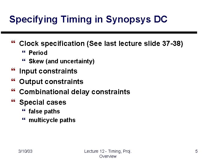
Specifying Timing in Synopsys DC } Clock specification (See last lecture slide 37 -38) } Period } Skew (and uncertainty) } } Input constraints Output constraints Combinational delay constraints Special cases } false paths } multicycle paths 3/10/03 Lecture 12 - Timing, Proj. Overview 5

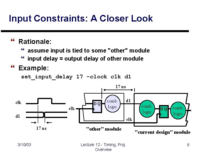
Input Constraints: A Closer Look } Rationale: } assume input is tied to some "other" module } input delay = output delay of other module } Example: set_input_delay 17 -clock clk d 1 17 ns clk DQ comb. logic d 1 DQ comb. logic clk 17 ns 3/10/03 comb. logic "other" module Lecture 12 - Timing, Proj. Overview "current design" module 6

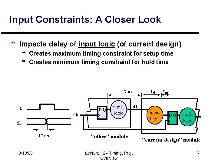
Input Constraints: A Closer Look } Impacts delay of input logic (of current design) } Creates maximum timing constraint for setup time } Creates minimum timing constraint for hold time tci 17 ns clk DQ comb. logic d 1 17 ns 3/10/03 tsu "other" module Lecture 12 - Timing, Proj. Overview input logic DQ comb. logic "current design" module 7

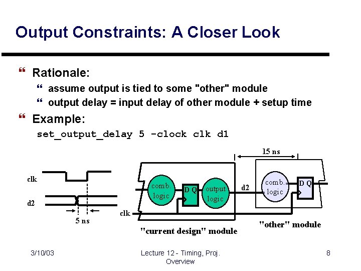
Output Constraints: A Closer Look } Rationale: } assume output is tied to some "other" module } output delay = input delay of other module + setup time } Example: set_output_delay 5 -clock clk d 1 15 ns clk comb. logic d 2 5 ns DQ output logic comb. logic DQ clk "current design" module 3/10/03 d 2 Lecture 12 - Timing, Proj. Overview "other" module 8

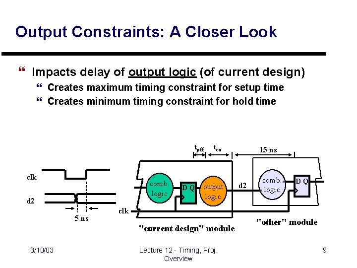
Output Constraints: A Closer Look } Impacts delay of output logic (of current design) } Creates maximum timing constraint for setup time } Creates minimum timing constraint for hold time tpff clk comb. logic d 2 5 ns DQ tco output logic d 2 comb. logic DQ clk "current design" module 3/10/03 15 ns Lecture 12 - Timing, Proj. Overview "other" module 9

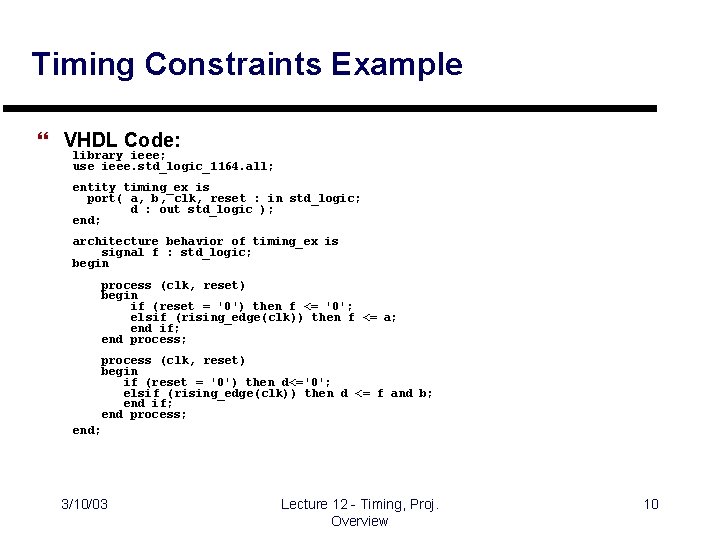
Timing Constraints Example } VHDL Code: library ieee; use ieee. std_logic_1164. all; entity timing_ex is port( a, b, clk, reset : in std_logic; d : out std_logic ); end; architecture behavior of timing_ex is signal f : std_logic; begin process (clk, reset) begin if (reset = '0') then f <= '0'; elsif (rising_edge(clk)) then f <= a; end if; end process; process (clk, reset) begin if (reset = '0') then d<='0'; elsif (rising_edge(clk)) then d <= f and b; end if; end process; end; 3/10/03 Lecture 12 - Timing, Proj. Overview 10

Timing Constraints Example } Timing Constraints: create_clock clk -period 10. 0 set_fix_hold clk /* check hold time */ set_input_delay 0. 5 -clock clk {a, b} set_output_delay 1. 0 -clock clk d; } Synthesized Design: 3/10/03 Lecture 12 - Timing, Proj. Overview 11

Getting Timing Reports: } Seeing timing results: report_timing command report_timing -max_paths 5 } Result: ******************** Report : timing -path full -delay max -max_paths 5 Design : timing_ex Version: 2000. 05 -1 Date : Thu Apr 5 15: 26: 05 2001 ******************** Operating Conditions: Wire Load Model Mode: top (continued) 3/10/03 Lecture 12 - Timing, Proj. Overview 12

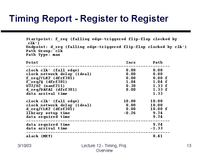
Timing Report - Register to Register Startpoint: f_reg (falling edge-triggered flip-flop clocked by clk') Endpoint: d_reg (falling edge-triggered flip-flop clocked by clk') Path Group: clk Path Type: max Point Incr Path -----------------------------clock clk' (fall edge) 0. 00 clock network delay (ideal) 0. 00 f_reg/CLK 2 (dfrf 301) 0. 00 f f_reg/Q (dfrf 301) 1. 04 f U 32/O 2 (nanf 211) 0. 30 1. 33 f d_reg/DATA 1 (dfrf 301) 0. 00 1. 33 f data arrival time 1. 33 clock clk' (fall edge) 10. 00 clock network delay (ideal) 0. 00 10. 00 d_reg/CLK 2 (dfrf 301) 0. 00 10. 00 f library setup time -0. 26 9. 74 data required time 9. 74 -----------------------------data required time 9. 74 data arrival time -1. 33 -----------------------------slack (MET) 8. 41 3/10/03 Lecture 12 - Timing, Proj. Overview 13

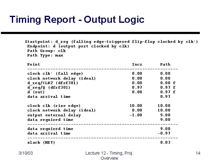
Timing Report - Output Logic Startpoint: d_reg (falling edge-triggered flip-flop clocked by clk') Endpoint: d (output port clocked by clk) Path Group: clk Path Type: max Point Incr Path -----------------------------clock clk' (fall edge) 0. 00 clock network delay (ideal) 0. 00 d_reg/CLK 2 (dfrf 301) 0. 00 f d_reg/Q (dfrf 301) 0. 97 f d (out) 0. 00 0. 97 f data arrival time 0. 97 clock clk (rise edge) 10. 00 clock network delay (ideal) 0. 00 10. 00 output external delay -1. 00 9. 00 data required time 9. 00 -----------------------------data required time 9. 00 data arrival time -0. 97 -----------------------------slack (MET) 8. 03 3/10/03 Lecture 12 - Timing, Proj. Overview 14

Timing Report - Input Logic Startpoint: a (input port clocked by clk) Endpoint: f_reg (falling edge-triggered flip-flop clocked by clk') Path Group: clk Path Type: max Point Incr Path -----------------------------clock clk (rise edge) 0. 00 clock network delay (ideal) 0. 00 input external delay 0. 50 f a (in) 0. 00 0. 50 f f_reg/DATA 1 (dfrf 301) 0. 00 0. 50 f data arrival time 0. 50 clock clk' (fall edge) 10. 00 clock network delay (ideal) 0. 00 10. 00 f_reg/CLK 2 (dfrf 301) 0. 00 10. 00 f library setup time -0. 23 9. 77 data required time 9. 77 -----------------------------data required time 9. 77 data arrival time -0. 50 -----------------------------slack (MET) 9. 27 3/10/03 Lecture 12 - Timing, Proj. Overview 15

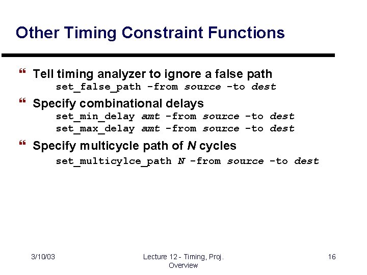
Other Timing Constraint Functions } Tell timing analyzer to ignore a false path set_false_path -from source -to dest } Specify combinational delays set_min_delay amt -from source -to dest set_max_delay amt -from source -to dest } Specify multicycle path of N cycles set_multicylce_path N -from source -to dest 3/10/03 Lecture 12 - Timing, Proj. Overview 16

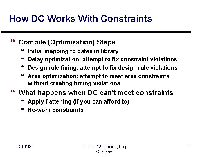
How DC Works With Constraints } Compile (Optimization) Steps } } Initial mapping to gates in library Delay optimization: attempt to fix constraint violations Design rule fixing: attempt to fix design rule violations Area optimization: attempt to meet area constraints without creating timing violations } What happens when DC can't meet constraints } Apply flattening (if you can afford to) } Re-work constraints 3/10/03 Lecture 12 - Timing, Proj. Overview 17

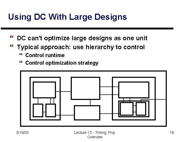
Using DC With Large Designs } DC can't optimize large designs as one unit } Typical approach: use hierarchy to control } Control runtime } Control optimization strategy 3/10/03 Lecture 12 - Timing, Proj. Overview 18

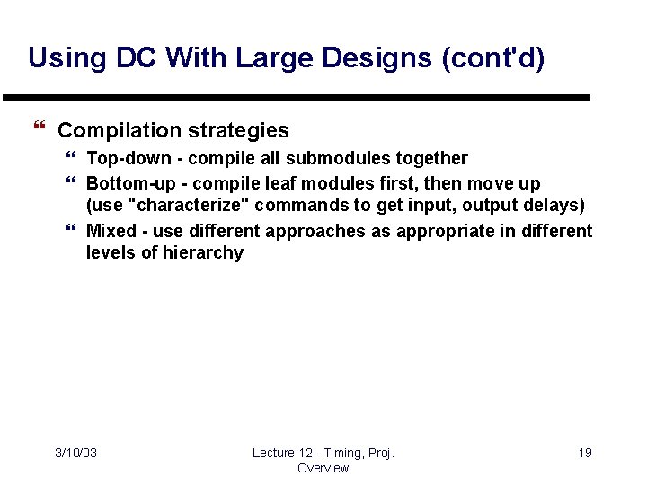
Using DC With Large Designs (cont'd) } Compilation strategies } Top-down - compile all submodules together } Bottom-up - compile leaf modules first, then move up (use "characterize" commands to get input, output delays) } Mixed - use different approaches as appropriate in different levels of hierarchy 3/10/03 Lecture 12 - Timing, Proj. Overview 19

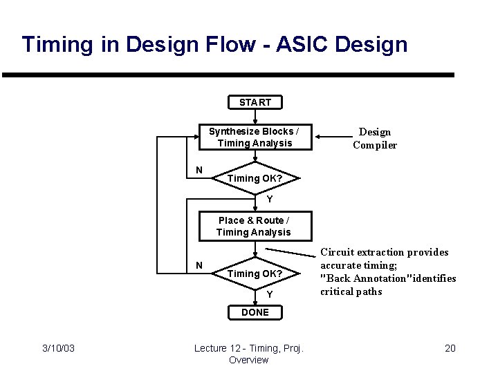
Timing in Design Flow - ASIC Design START Synthesize Blocks / Timing Analysis N Design Compiler Timing OK? Y Place & Route / Timing Analysis N Timing OK? Y Circuit extraction provides accurate timing; "Back Annotation"identifies critical paths DONE 3/10/03 Lecture 12 - Timing, Proj. Overview 20

Project Overview - Wimp. Net 03 } Key idea: computers communicate on shared wires (ether) } Each computer has 8 -bit address } Information passed as packets 3/10/03 Lecture 12 - Timing, Proj. Overview 21

Packet Format } Header } destination address (8 bits) } source address (8 bits) } length (8 bits) } Data - up to 255 bytes } CRC Byte - Error Code All bytes transmitted with LSB first 3/10/03 Lecture 12 - Timing, Proj. Overview 22

Control Procedure - CSMA/CD } Carrier Sense Multiple Access with Collision Detection } Procedure } Defer - don’t transmit when carrier sense } Transmit - transmit while monitoring data } Collision - error in transmission when two stations transmit at same time } Abort - terminate transmission and jam 4 -6 bytes } Backoff - wait for a random retransmission delay } Retransmit - try again after backoff 3/10/03 Lecture 12 - Timing, Proj. Overview 23

Project Goals } Build a complete Wimp. Net 03 Interface Chip } Receiver with buffer RAM } Transmitter with buffer RAM } Area budget: 4 MOSIS Tiny Chips (4400 l X 4400 l) 3/10/03 Lecture 12 - Timing, Proj. Overview 24

Transmitter Details 3/10/03 Lecture 12 - Timing, Proj. Overview 25

Receiver Details 3/10/03 Lecture 12 - Timing, Proj. Overview 26

RAM Subsystem Details } Two-port organization } Write port - writes on falling edge of clk when w_en_l=L } Read port } Size: 256 Bytes 3/10/03 Lecture 12 - Timing, Proj. Overview 27

Design Groups } } Receiver Design Transmitter Design RAM Subsystem Design Chip assembly 3/10/03 Lecture 12 - Timing, Proj. Overview 28

Coming Up } More about the Project } Subsystem Design: RAM 3/10/03 Lecture 12 - Timing, Proj. Overview 29