ECE 425 VLSI Circuit Design Lecture 7 Combinational
ECE 425 - VLSI Circuit Design Lecture 7 Combinational Logic Spring 2007 Prof. John Nestor ECE Department Lafayette College Easton, Pennsylvania 18042 nestorj@lafayette. edu ECE 425 Spring 2007 Lecture 7 - Comb. Logic 1
Announcements } Homework due Friday 2/23: } 2 -2, 2 -5, 2 -6, 2 -7, 2 -8, 2 -9, 2 -12, 2 -13, 2 -20 } Entrance Exam due Friday 2/23 } Reading } Wolf 3. 1 -3. 4 } Exam 1: Wednesday, March 8 ECE 425 Spring 2007 Lecture 7 - Comb. Logic 2
Where we are. . . } Last Time: } ASIC Design • Standard Cells • Gate Arrrays • FPGAs } Today: } Combinational Logic Design • Static CMOS: Delay, Noise Margin & Power ECE 425 Spring 2007 Lecture 7 - Comb. Logic 3
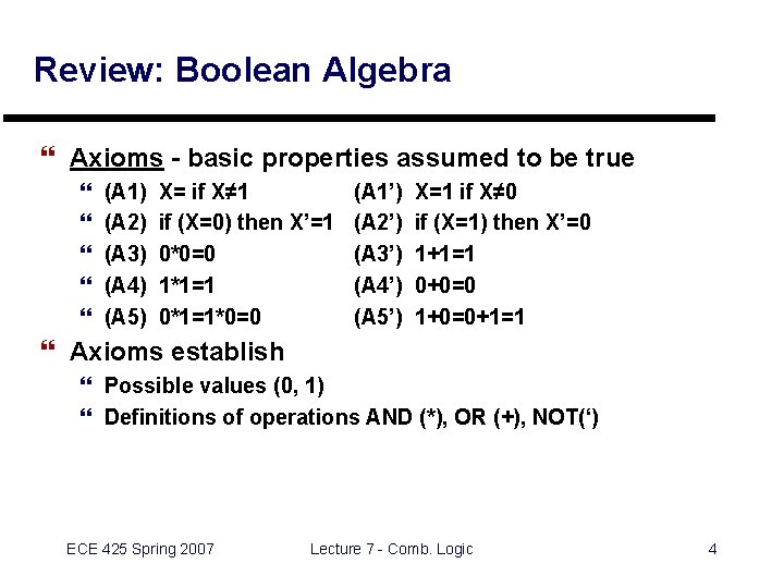
Review: Boolean Algebra } Axioms - basic properties assumed to be true } } } (A 1) (A 2) (A 3) (A 4) (A 5) X= if X≠ 1 if (X=0) then X’=1 0*0=0 1*1=1 0*1=1*0=0 (A 1’) (A 2’) (A 3’) (A 4’) (A 5’) X=1 if X≠ 0 if (X=1) then X’=0 1+1=1 0+0=0 1+0=0+1=1 } Axioms establish } Possible values (0, 1) } Definitions of operations AND (*), OR (+), NOT(‘) ECE 425 Spring 2007 Lecture 7 - Comb. Logic 4
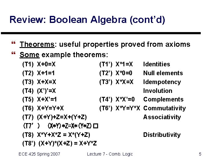
Review: Boolean Algebra (cont’d) } Theorems: useful properties proved from axioms } Some example theorems: (T 1) X+0=X (T 1’) (T 2) X+1=1 (T 2’) (T 3) X+X=X (T 3’) (T 4) (X’)’=X (T 5) X+X’=1 (T 4’) (T 6) X+Y=Y+X (T 6’) (T 7) (X+Y)+Z=X+(Y+Z) (T 7’) (X*Y)*Z=X*(Y*Z)� (T 8) X*Y+X*Z = X*(Y+Z) (T 8’) (X+Y)*(X+Z) = X+Y*Z ECE 425 Spring 2007 X*1=X X*0=0 X*X=X Identities Null elements Idempotency Involution X*X’=0 Complements X*Y=Y*X Commutativity Associativity Lecture 7 - Comb. Logic Distributivity 5
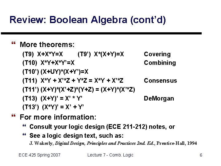
Review: Boolean Algebra (cont’d) } More theorems: (T 9) X+X*Y=X (T 9’) X*(X+Y)=X (T 10) X*Y+X*Y’=X (T 10’) (X+UY)*(X+Y’)=X (T 11) X*Y + X’*Z + Y*Z = X*Y + X’*Z (T 11’) (X+Y)*(X’+Z)*(Y+Z) = (X+Y)*(X’*Z) (T 13) (X+Y)’ = X’ * Y’ (T 13’) (X*Y)’ = X’ + Y’ Covering Combining Consensus De. Morgan } For more information: } Consult your logic design (ECE 211 -212) notes, or } See a logic design text, such as: J. Wakerly, Digital Design, Principles and Practices 2 nd. Ed. , Prentice-Hall, 1994 ECE 425 Spring 2007 Lecture 7 - Comb. Logic 6
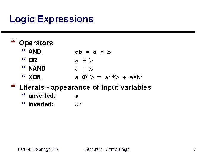
Logic Expressions } Operators } } AND OR NAND XOR ab = a * b a + b a | b a Å b = a’*b + a*b’ } Literals - appearance of input variables } unverted: } inverted: ECE 425 Spring 2007 a a' Lecture 7 - Comb. Logic 7
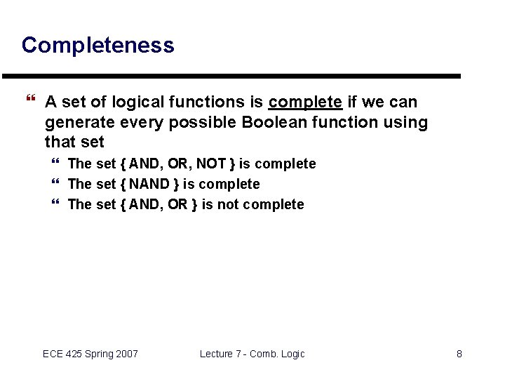
Completeness } A set of logical functions is complete if we can generate every possible Boolean function using that set } The set { AND, OR, NOT } is complete } The set { NAND } is complete } The set { AND, OR } is not complete ECE 425 Spring 2007 Lecture 7 - Comb. Logic 8
Irredundancy } A logical expression is irredundant if no literal can be removed from the expression without changings its value } Redundant expressions: a*b + a*b' } Irredundant expressions: a*b' + a'*b a + c*d' ECE 425 Spring 2007 Lecture 7 - Comb. Logic 9
Minimality } A logic expression is minimal if no equivalent form has a higher cost (i. e. , literal count) } Minimality ≠ Irredundancy } CAD tools are available to find the minimal (or nearminimal) form for: } Two level logic (AND/OR Sum of Products) } Multilevel Logic (Arbitrary network of gates) ECE 425 Spring 2007 Lecture 7 - Comb. Logic 10

Review - Complementary CMOS } Pullup Network - drives output to VDD } Pulldown Network - drives output to GND ECE 425 Spring 2007 Lecture 7 - Comb. Logic 11
Complementary CMOS Notes } Pullup, pulldown networks should NEVER conduct at same time! } Pullup, pulldown networks are duals } Parallel in pulldown implies serial in pullup } Serial in pulldown implies parallel in pullup } Gate Types: } Simple: NAND, NOR, inverter } And-Or-Invert (AOI) } Or-And-Invert (OAI) ECE 425 Spring 2007 Lecture 7 - Comb. Logic 12
Layout Considerations } Metal lines required for Vdd!, Gnd! } ndiff, pdiff must be separated by 10 lambda } Transistor options: } horizontal or vertical diffusion lines } Start with minimum-size transistors • Increased width implies increased driving capability, but • Do the analysis first to see if it’s necessary ECE 425 Spring 2007 Lecture 7 - Comb. Logic 13
Layout Considerations (cont'd) } Interconnect layers (use vias when necessary): } } Metal 1 Metal 2 Poly Diffusion } Specify a well depending on process type } Use substrate contacts to bias transistors & prevent latchup ECE 425 Spring 2007 Lecture 7 - Comb. Logic 14
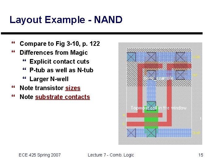
Layout Example - NAND } Compare to Fig 3 -10, p. 122 } Differences from Magic } Explicit contact cuts } P-tub as well as N-tub } Larger N-well } Note transistor sizes } Note substrate contacts ECE 425 Spring 2007 Lecture 7 - Comb. Logic 15
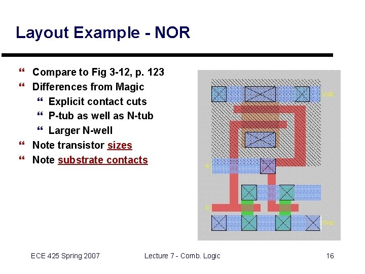
Layout Example - NOR } Compare to Fig 3 -12, p. 123 } Differences from Magic } Explicit contact cuts } P-tub as well as N-tub } Larger N-well } Note transistor sizes } Note substrate contacts ECE 425 Spring 2007 Lecture 7 - Comb. Logic 16
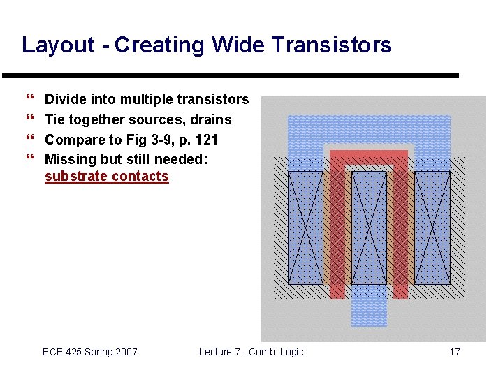
Layout - Creating Wide Transistors } } Divide into multiple transistors Tie together sources, drains Compare to Fig 3 -9, p. 121 Missing but still needed: substrate contacts ECE 425 Spring 2007 Lecture 7 - Comb. Logic 17
Review - CMOS Gate Structure ECE 425 Spring 2007 Lecture 7 - Comb. Logic 18
Inverter - DC Analysis A B in out C D E ECE 425 Spring 2007 Lecture 7 - Comb. Logic 19
Inverter DC Analysis - Continued A B C D E Note dependence on bn/bp Recall: Source: N. Weste & K. Eshraghian, Principles of CMOS VLSI Design Addison Wesley, 1992 ECE 425 Spring 2007 Lecture 7 - Comb. Logic 20
Logic Levels: Output } Logic values are represented by a range of voltages } Logic 1: between VOH and VDD (5 V) } Logic 0: between VOL and VSS (0 V) } Static CMOS Output levels } VOH = VDD (5 V) } VOL = VSS = Gnd (0 V) ECE 425 Spring 2007 Lecture 7 - Comb. Logic 21
Logic Levels: Input } Examine DC Input/Output Curve (Fig 3 -15, p. 120) } Pick points where slope = -1 as VIL , VIH } Rationale: compare change in VIN , VOUT } VIN < VIL small change in VIN causes small change in VOUT } VIN > VOUT small change in VIN causes small change in VOUT } VIN < VIL < VIH small change in VIN causes large change in VOUT ECE 425 Spring 2007 Lecture 7 - Comb. Logic 22

Logic Levels - Summary ECE 425 Spring 2007 Lecture 7 - Comb. Logic 23
Noise Margin } A measure of noise immunity } Logic 1: NMH = VOH - VIH } Logic 0: NML = VOL - VIL } Important when noise is present } Definition: small random variations in voltage } Don’t want noise to affect circuit output ECE 425 Spring 2007 Lecture 7 - Comb. Logic 24
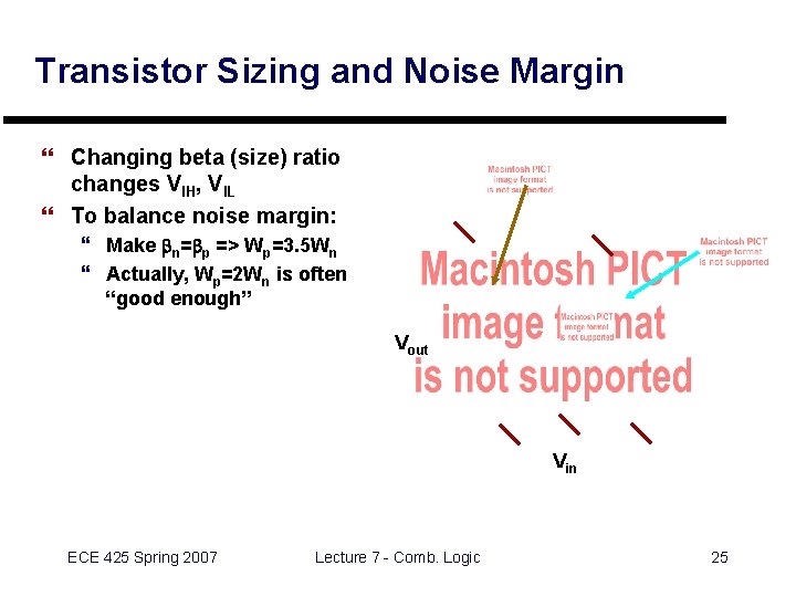
Transistor Sizing and Noise Margin } Changing beta (size) ratio changes VIH, VIL } To balance noise margin: } Make bn=bp => Wp=3. 5 Wn } Actually, Wp=2 Wn is often “good enough” Vout Vin ECE 425 Spring 2007 Lecture 7 - Comb. Logic 25
Coming Up } } } Delay Calculation Body effect Power Consumption Power-speed product Parasitics and delay ECE 425 Spring 2007 Lecture 7 - Comb. Logic 26
- Slides: 26