ECE 425 VLSI Circuit Design Lecture 4 Layout
- Slides: 27

ECE 425 - VLSI Circuit Design Lecture 4 - Layout & Design Rules Spring 2007 Prof. John Nestor ECE Department Lafayette College Easton, Pennsylvania 18042 nestorj@lafayette. edu ECE 425 Spring 2007 Lecture 4 - Layout & Design Rules 1

Announcements } Reading } Wolf 2. 4 -2. 6 ECE 425 Spring 2007 Lecture 4 - Layout & Design Rules 2

Where we are. . . } Last time: } Transistor Modes of Operation } More about Wires & Vias } Parasitics } Today: } Parasitics continued (Lecture 3 pp. 28 -40) } Layout & Design Rules; Stick Diagrams } Discuss Lab 3 ECE 425 Spring 2007 Lecture 4 - Layout & Design Rules 3

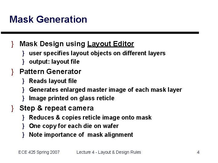
Mask Generation } Mask Design using Layout Editor } user specifies layout objects on different layers } output: layout file } Pattern Generator } Reads layout file } Generates enlarged master image of each mask layer } Image printed on glass reticle } Step & repeat camera } Reduces & copies reticle image onto mask } One copy for each die on wafer } Note importance of mask alignment ECE 425 Spring 2007 Lecture 4 - Layout & Design Rules 4

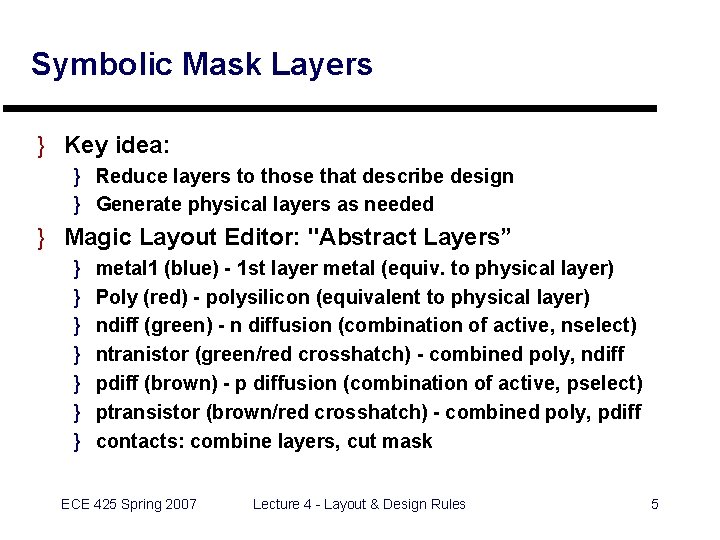
Symbolic Mask Layers } Key idea: } Reduce layers to those that describe design } Generate physical layers as needed } Magic Layout Editor: "Abstract Layers” } } } } metal 1 (blue) - 1 st layer metal (equiv. to physical layer) Poly (red) - polysilicon (equivalent to physical layer) ndiff (green) - n diffusion (combination of active, nselect) ntranistor (green/red crosshatch) - combined poly, ndiff pdiff (brown) - p diffusion (combination of active, pselect) ptransistor (brown/red crosshatch) - combined poly, pdiff contacts: combine layers, cut mask ECE 425 Spring 2007 Lecture 4 - Layout & Design Rules 5

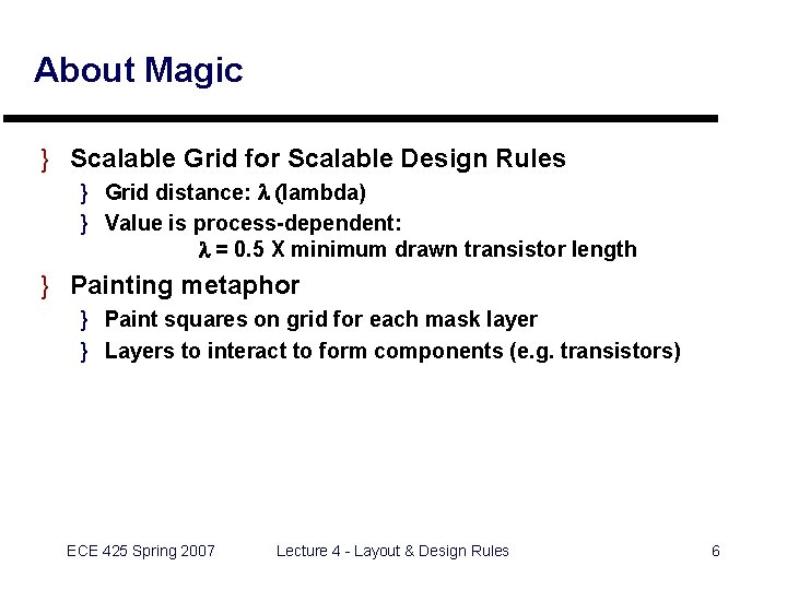
About Magic } Scalable Grid for Scalable Design Rules } Grid distance: l (lambda) } Value is process-dependent: l = 0. 5 X minimum drawn transistor length } Painting metaphor } Paint squares on grid for each mask layer } Layers to interact to form components (e. g. transistors) ECE 425 Spring 2007 Lecture 4 - Layout & Design Rules 6

Mask Layers in Magic } } } } Poly (red) N Diffusion (green) P Diffusion (brown) Metal (blue) Metal 2 (purple) Well (cross-hatching) Contacts (X) ECE 425 Spring 2007 Lecture 4 - Layout & Design Rules 7

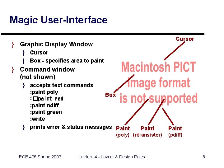
Magic User-Interface Cursor } Graphic Display Window } Cursor } Box - specifies area to paint } Command window (not shown) } accepts text commands : paint poly Box : �paint red : paint ndiff : paint green : write } prints error & status messages Paint (poly) (ntransistor) ECE 425 Spring 2007 Lecture 4 - Layout & Design Rules Paint (pdiff) 8

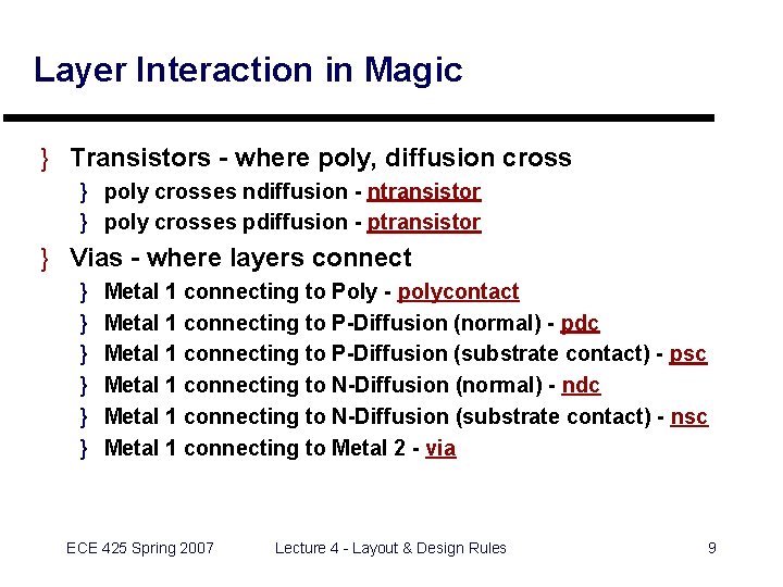
Layer Interaction in Magic } Transistors - where poly, diffusion cross } poly crosses ndiffusion - ntransistor } poly crosses pdiffusion - ptransistor } Vias - where layers connect } } } Metal 1 connecting to Poly - polycontact Metal 1 connecting to P-Diffusion (normal) - pdc Metal 1 connecting to P-Diffusion (substrate contact) - psc Metal 1 connecting to N-Diffusion (normal) - ndc Metal 1 connecting to N-Diffusion (substrate contact) - nsc Metal 1 connecting to Metal 2 - via ECE 425 Spring 2007 Lecture 4 - Layout & Design Rules 9

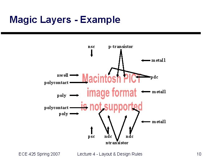
Magic Layers - Example nsc p-transistor metal 1 nwell pdc polycontact metal 1 polycontact poly metal 1 psc ECE 425 Spring 2007 ndc ntransistor Lecture 4 - Layout & Design Rules 10

Lab 2 - Introduction to Magic } Preparation } Read Prof. Stine’s Magic Tutorial } Read Magic Tutorials 1 & 2 } In the Lab } } Use the PCs running Linux - log in with CS account Do “Step by Step Example” in Magic Tutorial Create a layout for a 3 -input NAND gate Plot and hand in ECE 425 Spring 2007 Lecture 4 - Layout & Design Rules 11

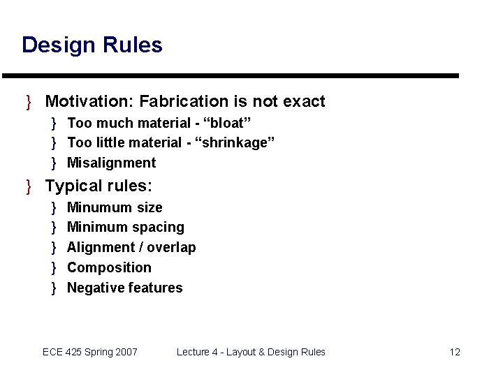
Design Rules } Motivation: Fabrication is not exact } Too much material - “bloat” } Too little material - “shrinkage” } Misalignment } Typical rules: } } } Minumum size Minimum spacing Alignment / overlap Composition Negative features ECE 425 Spring 2007 Lecture 4 - Layout & Design Rules 12

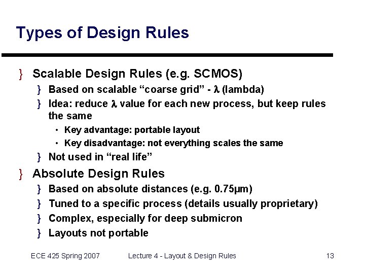
Types of Design Rules } Scalable Design Rules (e. g. SCMOS) } Based on scalable “coarse grid” - l (lambda) } Idea: reduce l value for each new process, but keep rules the same • Key advantage: portable layout • Key disadvantage: not everything scales the same } Not used in “real life” } Absolute Design Rules } } Based on absolute distances (e. g. 0. 75µm) Tuned to a specific process (details usually proprietary) Complex, especially for deep submicron Layouts not portable ECE 425 Spring 2007 Lecture 4 - Layout & Design Rules 13

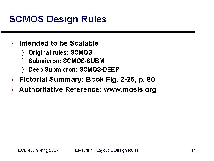
SCMOS Design Rules } Intended to be Scalable } Original rules: SCMOS } Submicron: SCMOS-SUBM } Deep Submicron: SCMOS-DEEP } Pictorial Summary: Book Fig. 2 -26, p. 80 } Authoritative Reference: www. mosis. org ECE 425 Spring 2007 Lecture 4 - Layout & Design Rules 14

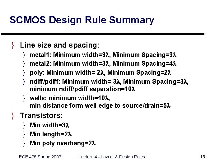
SCMOS Design Rule Summary } Line size and spacing: } } metal 1: Minimum width=3 l, Minimum Spacing=3 l metal 2: Minimum width=3 l, Minimum Spacing=4 l poly: Minimum width= 2 l, Minimum Spacing=2 l ndiff/pdiff: Minimum width= 3 l, Minimum Spacing=3 l, minimum ndiff/pdiff seperation=10 l } wells: minimum width=10 l, min distance form well edge to source/drain=5 l } Transistors: } Min width=3 l } Min length=2 l } Min poly overhang=2 l ECE 425 Spring 2007 Lecture 4 - Layout & Design Rules 15

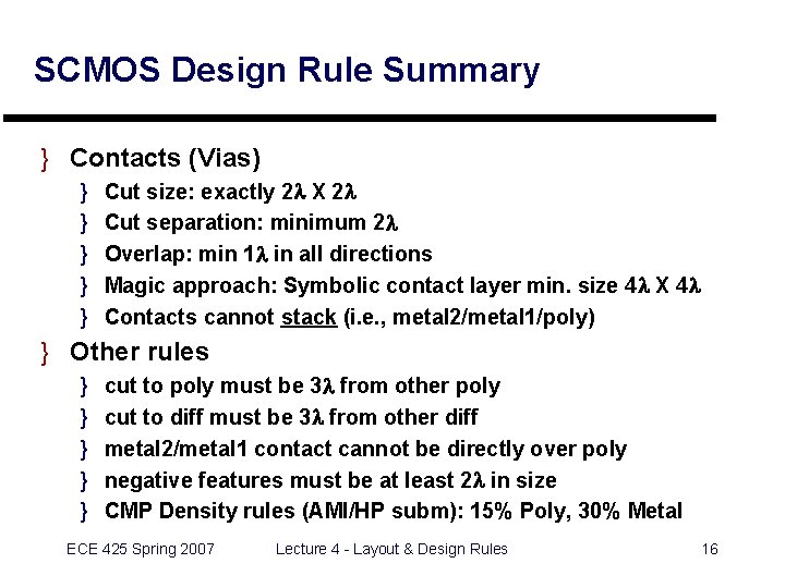
SCMOS Design Rule Summary } Contacts (Vias) } } } Cut size: exactly 2 l X 2 l Cut separation: minimum 2 l Overlap: min 1 l in all directions Magic approach: Symbolic contact layer min. size 4 l X 4 l Contacts cannot stack (i. e. , metal 2/metal 1/poly) } Other rules } } } cut to poly must be 3 l from other poly cut to diff must be 3 l from other diff metal 2/metal 1 contact cannot be directly over poly negative features must be at least 2 l in size CMP Density rules (AMI/HP subm): 15% Poly, 30% Metal ECE 425 Spring 2007 Lecture 4 - Layout & Design Rules 16

Design Rule Checking in Magic } Design violations displayed as error paint } Find which rule is violated with ": drc why” Poly must overhang transistor by at least 2 (MOSIS rule #3. 3) ECE 425 Spring 2007 Lecture 4 - Layout & Design Rules 17

Stick Diagrams } Key idea: "Stick figure cartoon" of a layout } Useful for planning layout } } relative placement of transistors assignment of signals to layers connections between cells cell hierarchy ECE 425 Spring 2007 Lecture 4 - Layout & Design Rules 18

Stick Diagrams (cont'd) ECE 425 Spring 2007 Lecture 4 - Layout & Design Rules 19

Stick Diagram Examples ECE 425 Spring 2007 Lecture 4 - Layout & Design Rules 20

Stick Diagram Examples ECE 425 Spring 2007 Lecture 4 - Layout & Design Rules 21

Example: Layout / Stick Diagram } Create a layout for a NAND gate given constraints: } Use minimum-size transistors } Assume power supply lines “pass through” cell from left to right at top and bottom of cell } Assume inputs are on left side of cell } Assume output is on right side of cell } Optimize cell to minimize width } Optimize cell to minimize overall area ECE 425 Spring 2007 Lecture 4 - Layout & Design Rules 22

Layout Example Circuit Diagram. ECE 425 Spring 2007 Exterior of Cell Lecture 4 - Layout & Design Rules 23

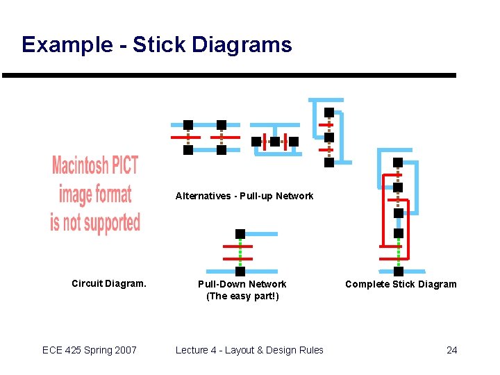
Example - Stick Diagrams Alternatives - Pull-up Network Circuit Diagram. ECE 425 Spring 2007 Pull-Down Network (The easy part!) Lecture 4 - Layout & Design Rules Complete Stick Diagram 24

Example - Magic Layout } Overall Layout: 52 X 16 ECE 425 Spring 2007 Lecture 4 - Layout & Design Rules 25

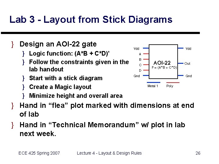
Lab 3 - Layout from Stick Diagrams } Design an AOI-22 gate } Logic function: (A*B + C*D)’ } Follow the constraints given in the lab handout } Start with a stick diagram } Create a Magic layout } Minimize height and overall area } Hand in “flea” plot marked with dimensions at end of lab } Hand in “Technical Memorandum” w/ plot in lab next week. ECE 425 Spring 2007 Lecture 4 - Layout & Design Rules 26

Coming Up: } } Hierarchical Layout Review: Levels of Abstraction More Layout CAD Tools: Extraction, LVS ASIC Layout Styles ECE 425 Spring 2007 Lecture 4 - Layout & Design Rules 27