ECE 425 VLSI Circuit Design Lecture 21 Floorplanning

- Slides: 40

ECE 425 - VLSI Circuit Design Lecture 21 - Floorplanning Spring, 2007 Prof. John Nestor ECE Department Lafayette College Easton, Pennsylvania 18042 nestorj@lafayette. edu ECE 425 Spring 2007 Lecture 21 - Floorplanning 1

Announcements } Reading } Book: 7. 1 - 7. 4 } Where We Are } Last Time: • Packaging • I/O Pads • MOSIS Pad Cells and the Project Pad Frame } Today • Floorplanning ECE 425 Spring 2007 Lecture 21 - Floorplanning 2

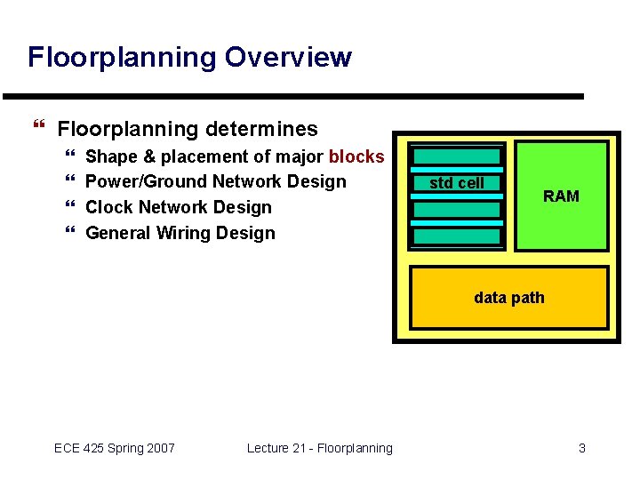
Floorplanning Overview } Floorplanning determines } } Shape & placement of major blocks Power/Ground Network Design Clock Network Design General Wiring Design std cell RAM data path ECE 425 Spring 2007 Lecture 21 - Floorplanning 3

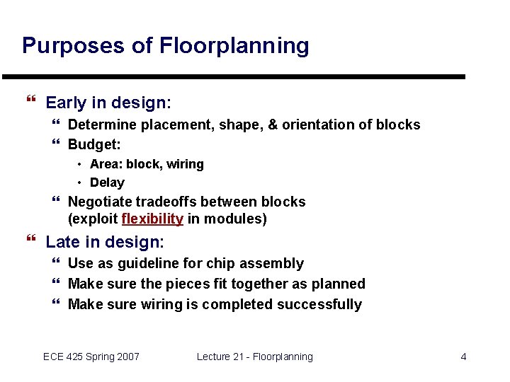
Purposes of Floorplanning } Early in design: } Determine placement, shape, & orientation of blocks } Budget: • Area: block, wiring • Delay } Negotiate tradeoffs between blocks (exploit flexibility in modules) } Late in design: } Use as guideline for chip assembly } Make sure the pieces fit together as planned } Make sure wiring is completed successfully ECE 425 Spring 2007 Lecture 21 - Floorplanning 4

Floorplanning Concerns } Assign locations to blocks of different shapes and sizes } Wiring Concerns } } Location of routing regions Power/Ground Wiring Clock Wiring General connection wiring } Special case of the placement problem ECE 425 Spring 2007 Lecture 21 - Floorplanning 5

Block Placement } Blocks have: } } Area - usually fixed Aspect ratio - often changeable Orientation - may be rotated, reflected Location - physical location on chip } Goal: find a placement of all blocks that “fits” ECE 425 Spring 2007 Lecture 21 - Floorplanning 6

Blocks and Wiring } Cannot ignore wiring during block placement } Large wiring areas may force rearrangement of blocks. } Wiring plan must consider area and delay of critical signals. } Blocks divide wiring area into routing channels. ECE 425 Spring 2007 Lecture 21 - Floorplanning 7

Demonstration Simplified Floorplanning Applet } Blocks may be rotated, reflected } Wirelength estimated by “rat’s nest” } One possible algorithm: simulated annealing ECE 425 Spring 2007 Lecture 21 - Floorplanning 8

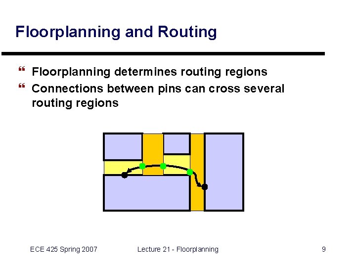
Floorplanning and Routing } Floorplanning determines routing regions } Connections between pins can cross several routing regions ECE 425 Spring 2007 Lecture 21 - Floorplanning 9

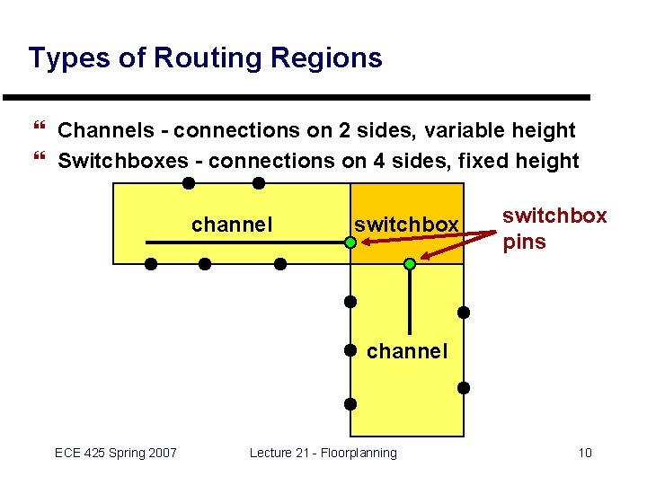
Types of Routing Regions } Channels - connections on 2 sides, variable height } Switchboxes - connections on 4 sides, fixed height channel switchbox pins channel ECE 425 Spring 2007 Lecture 21 - Floorplanning 10

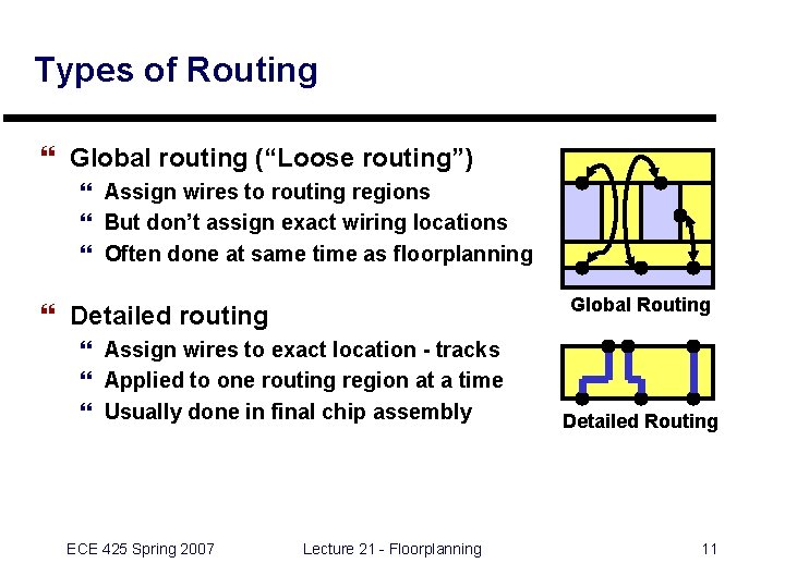
Types of Routing } Global routing (“Loose routing”) } Assign wires to routing regions } But don’t assign exact wiring locations } Often done at same time as floorplanning Global Routing } Detailed routing } Assign wires to exact location - tracks } Applied to one routing region at a time } Usually done in final chip assembly ECE 425 Spring 2007 Lecture 21 - Floorplanning Detailed Routing 11

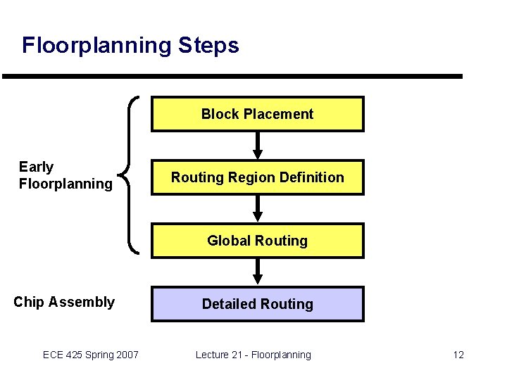
Floorplanning Steps Block Placement Early Floorplanning Routing Region Definition Global Routing Chip Assembly ECE 425 Spring 2007 Detailed Routing Lecture 21 - Floorplanning 12

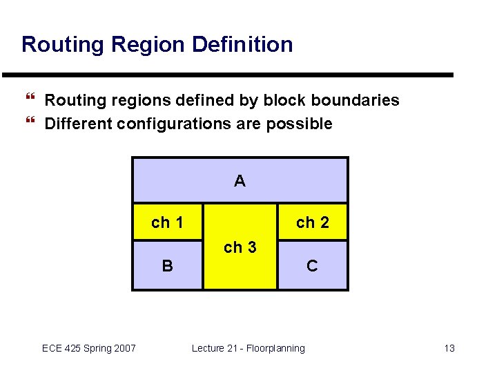
Routing Region Definition } Routing regions defined by block boundaries } Different configurations are possible A ECE 425 Spring 2007 ch 1 channel 1 ch 2 B ch 3 ch 2 C Lecture 21 - Floorplanning 13

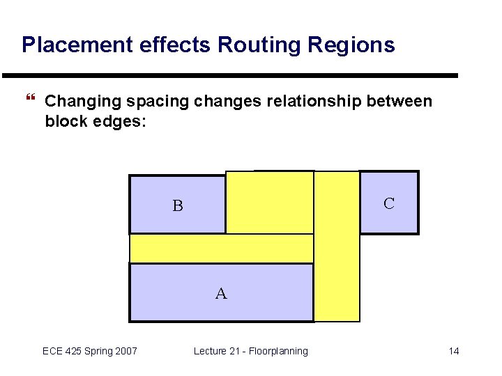
Placement effects Routing Regions } Changing spacing changes relationship between block edges: C B C A ECE 425 Spring 2007 Lecture 21 - Floorplanning 14

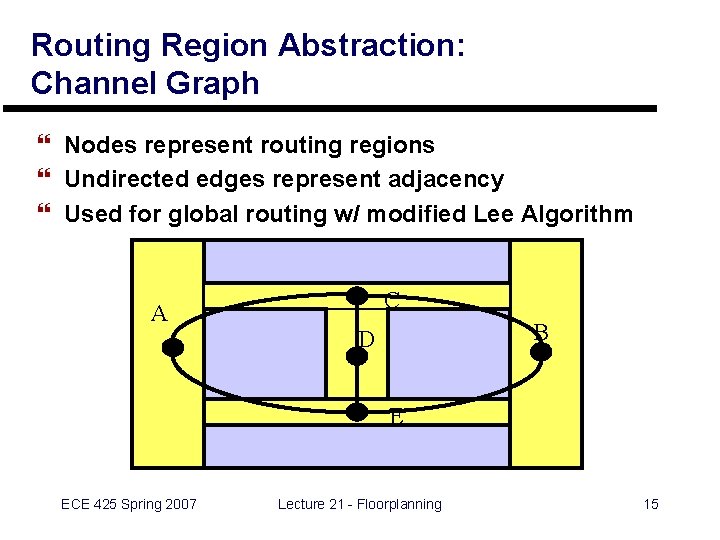
Routing Region Abstraction: Channel Graph } Nodes represent routing regions } Undirected edges represent adjacency } Used for global routing w/ modified Lee Algorithm A C B D E ECE 425 Spring 2007 Lecture 21 - Floorplanning 15

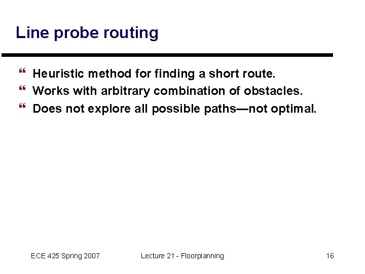
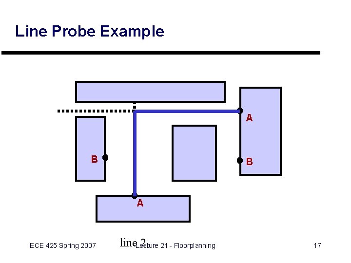
Line probe routing } Heuristic method for finding a short route. } Works with arbitrary combination of obstacles. } Does not explore all possible paths—not optimal. ECE 425 Spring 2007 Lecture 21 - Floorplanning 16

Line Probe Example A B B A ECE 425 Spring 2007 line. Lecture 2 21 - Floorplanning 17

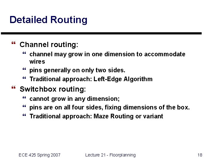
Detailed Routing } Channel routing: } channel may grow in one dimension to accommodate wires } pins generally on only two sides. } Traditional approach: Left-Edge Algorithm } Switchbox routing: } cannot grow in any dimension; } pins are on all four sides, fixing dimensions of the box. } Traditional approach: Maze Routing or variant ECE 425 Spring 2007 Lecture 21 - Floorplanning 18

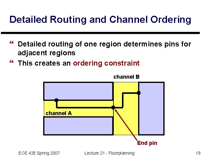
Detailed Routing and Channel Ordering } Detailed routing of one region determines pins for adjacent regions } This creates an ordering constraint channel B channel A End pin ECE 425 Spring 2007 Lecture 21 - Floorplanning 19

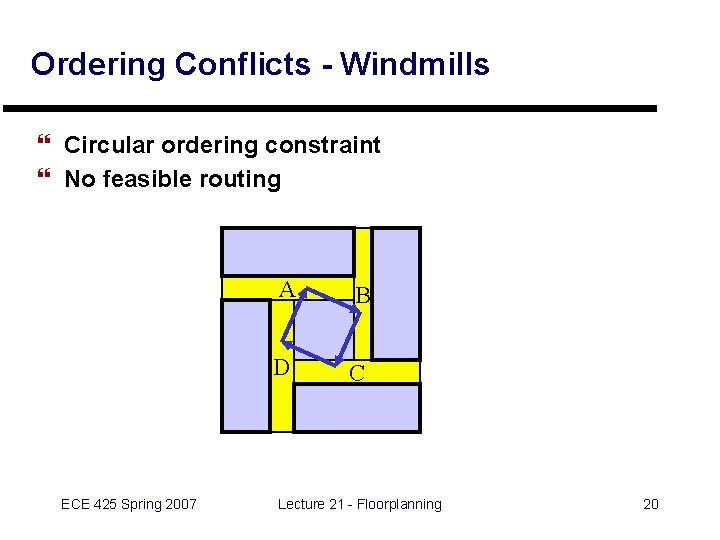
Ordering Conflicts - Windmills } Circular ordering constraint } No feasible routing ECE 425 Spring 2007 A B D C Lecture 21 - Floorplanning 20

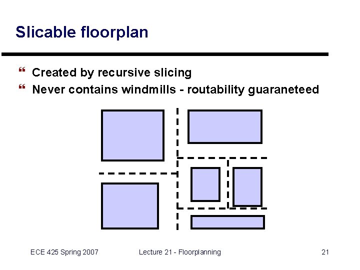
Slicable floorplan } Created by recursive slicing } Never contains windmills - routability guaraneteed ECE 425 Spring 2007 Lecture 21 - Floorplanning 21

Power distribution } Must size wires to be able to handle current— requires designing topology of VDD/Gnd networks. } Want to keep power network in metal—requires designing planar wiring. ECE 425 Spring 2007 Lecture 21 - Floorplanning 22

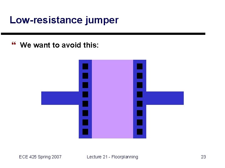
Low-resistance jumper } We want to avoid this: ` ECE 425 Spring 2007 Lecture 21 - Floorplanning 23

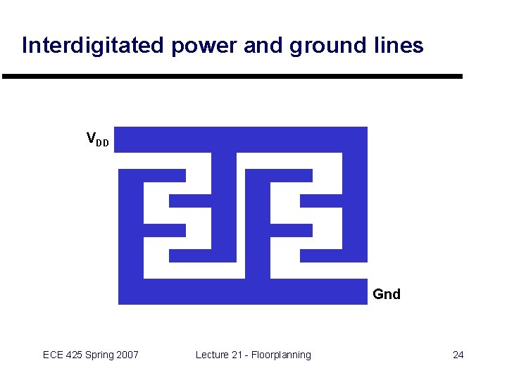
Interdigitated power and ground lines VDD Gnd ECE 425 Spring 2007 Lecture 21 - Floorplanning 24

Power tree design } Interdigitated power, ground trees } Recall rules for metal migration current density < 1. 5 m. A/µm } Each branch must be able to supply required current to all of its subsidiary branches } Size buses by recursively estimating peak currents ECE 425 Spring 2007 Lecture 21 - Floorplanning 25

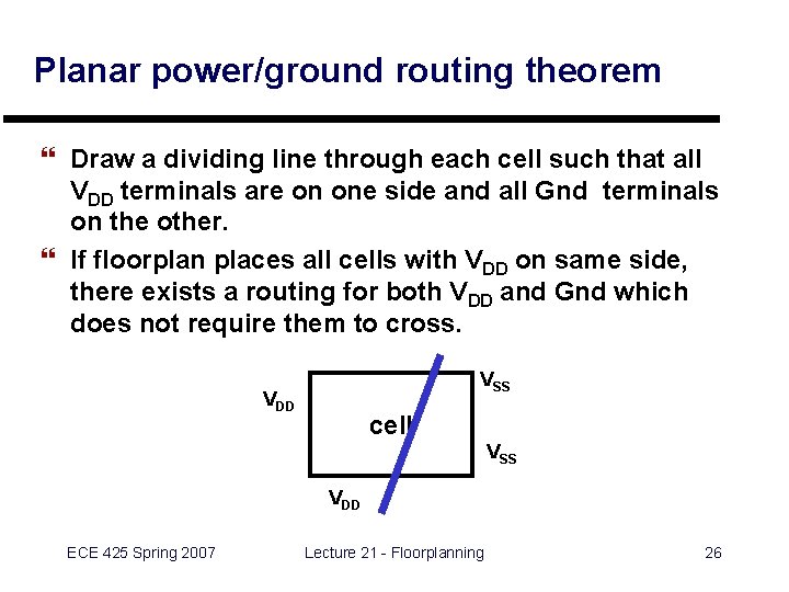
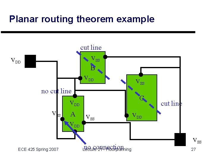
Planar power/ground routing theorem } Draw a dividing line through each cell such that all VDD terminals are on one side and all Gnd terminals on the other. } If floorplan places all cells with VDD on same side, there exists a routing for both VDD and Gnd which does not require them to cross. VSS VDD cell VSS VDD ECE 425 Spring 2007 Lecture 21 - Floorplanning 26

Planar routing theorem example cut line VSS VDD B VDD no cut line C VDD VSS A VDD ECE 425 Spring 2007 VSS no connection Lecture 21 - Floorplanning cut line VDD VSS 27

Power supply noise } Variations in power supply voltage manifest themselves as noise into the logic gates. } Power supply wiring resistance creates voltage variations with current surges. } Voltage drops on power lines depend on dynamic behavior of circuit. ECE 425 Spring 2007 Lecture 21 - Floorplanning 28

Tackling power supply noise } Must measure current required by each block at varying times. } May need to redesign power/ground network to reduce resistance at high current loads. } Worst case, may have to move some activity to another clock cycle to reduce peak current. ECE 425 Spring 2007 Lecture 21 - Floorplanning 29

Clock distribution } Goals: } deliver clock to all memory elements with acceptable skew; } deliver clock edges with acceptable sharpness. } Clocking network design is one of the greatest challenges in the design of a large chip. ECE 425 Spring 2007 Lecture 21 - Floorplanning 30

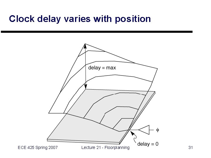
Clock delay varies with position ECE 425 Spring 2007 Lecture 21 - Floorplanning 31

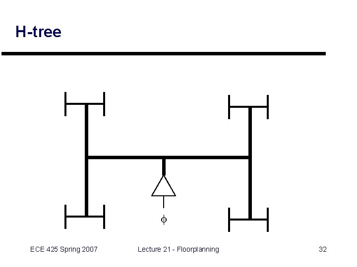
H-tree f ECE 425 Spring 2007 Lecture 21 - Floorplanning 32

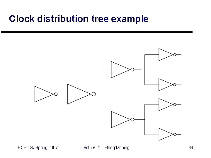
Clock distribution tree } Clocks are generally distributed via wiring trees. } Want to use low-resistance interconnect to minimize delay. } Use multiple drivers to distribute driver requirements—use optimal sizing principles to design buffers. } Clock lines can create significant crosstalk. ECE 425 Spring 2007 Lecture 21 - Floorplanning 33

Clock distribution tree example ECE 425 Spring 2007 Lecture 21 - Floorplanning 34

Floorplanning tips } Develop a wiring plan. Think about how layers will be used to distribute important wires. } Sweep small components into larger blocks. A floorplan with a single NAND gate in the middle will be hard to work with. } Design wiring that looks simple. If it looks complicated, it is complicated. ECE 425 Spring 2007 Lecture 21 - Floorplanning 35

Floorplanning tips, cont’d. } Design planar wiring. Planarity is the essence of simplicity. It isn’t always possible, but do it where feasible (and where it doesn’t introduce unacceptable delay). } Draw separate wiring plans for power and clocking. These are important design tasks which should be tackled early. ECE 425 Spring 2007 Lecture 21 - Floorplanning 36

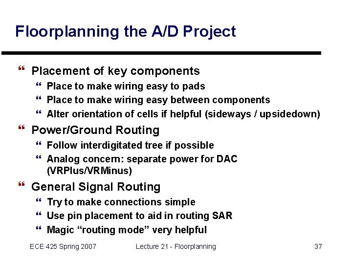
Floorplanning the A/D Project } Placement of key components } Place to make wiring easy to pads } Place to make wiring easy between components } Alter orientation of cells if helpful (sideways / upsidedown) } Power/Ground Routing } Follow interdigitated tree if possible } Analog concern: separate power for DAC (VRPlus/VRMinus) } General Signal Routing } Try to make connections simple } Use pin placement to aid in routing SAR } Magic “routing mode” very helpful ECE 425 Spring 2007 Lecture 21 - Floorplanning 37

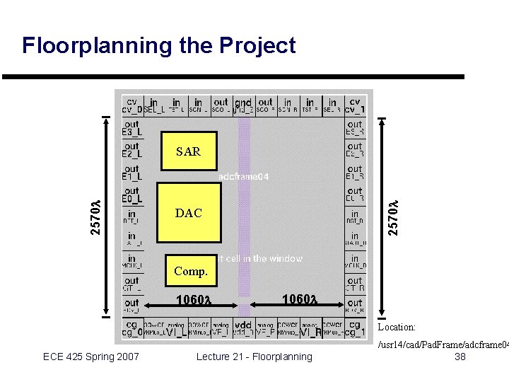
Floorplanning the Project 2570 l SAR DAC Comp. 1060 l Location: ECE 425 Spring 2007 Lecture 21 - Floorplanning /usr 14/cad/Pad. Frame/adcframe 04 38

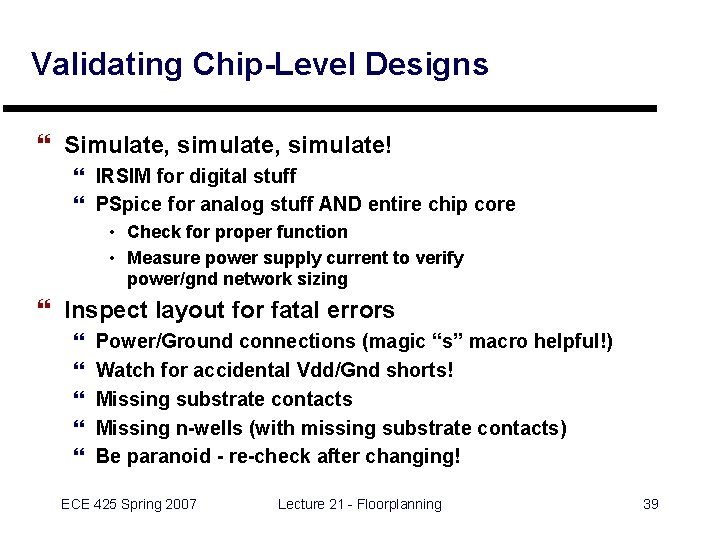
Validating Chip-Level Designs } Simulate, simulate! } IRSIM for digital stuff } PSpice for analog stuff AND entire chip core • Check for proper function • Measure power supply current to verify power/gnd network sizing } Inspect layout for fatal errors } } } Power/Ground connections (magic “s” macro helpful!) Watch for accidental Vdd/Gnd shorts! Missing substrate contacts Missing n-wells (with missing substrate contacts) Be paranoid - re-check after changing! ECE 425 Spring 2007 Lecture 21 - Floorplanning 39

Coming Up } Chip-Level Design: Case Studies } Subsystem Design ECE 425 Spring 2007 Lecture 21 - Floorplanning 40