ECE 425 VLSI Circuit Design Lecture 19 Architecture



- Slides: 41

ECE 425 - VLSI Circuit Design Lecture 19 - Architecture Design; Analog-Digital Conversion Spring 2007 Prof. John Nestor ECE Department Lafayette College Easton, Pennsylvania 18042 nestorj@lafayette. edu ECE 425 Spring 2007 Lecture 19 - Arch. Design, A/D 1

Announcements } Reading } Book: 8. 1 -8. 4, 7. 1 -7. 3 ECE 425 Spring 2007 Lecture 19 - Arch. Design, A/D 2

Where we are } Last Time: } Design for Test, Built-in Self Test } Today } } } System Design: Datapath/Controller Design Aside: Datapath/Controller Example in VHDL Comparators A/D Conversion Discuss Project ECE 425 Spring 2007 Lecture 19 - Arch. Design, A/D 3

The Datapath-Controller Abstraction } A higher-level description of chip organization } Key idea: break up design into two parts: } Datapath- components that manipulate data } Controller - FSM that controls datapath modules ECE 425 Spring 2007 Lecture 19 - Arch. Design, A/D 4

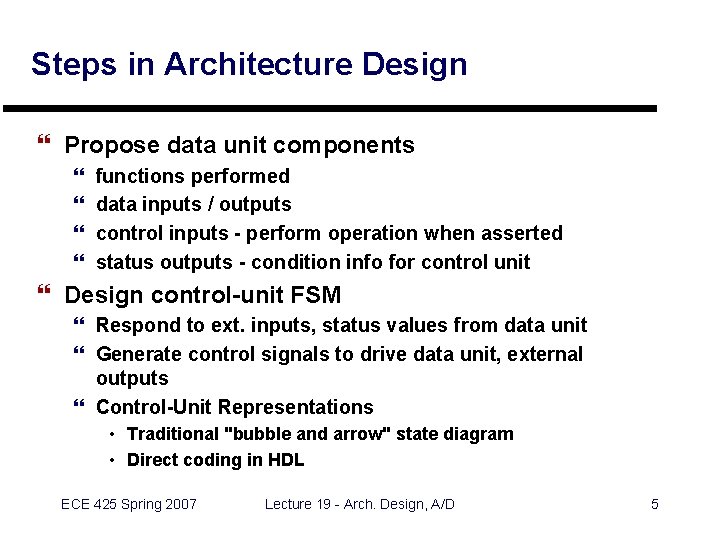
Steps in Architecture Design } Propose data unit components } } functions performed data inputs / outputs control inputs - perform operation when asserted status outputs - condition info for control unit } Design control-unit FSM } Respond to ext. inputs, status values from data unit } Generate control signals to drive data unit, external outputs } Control-Unit Representations • Traditional "bubble and arrow" state diagram • Direct coding in HDL ECE 425 Spring 2007 Lecture 19 - Arch. Design, A/D 5

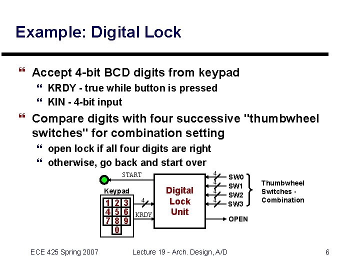
Example: Digital Lock } Accept 4 -bit BCD digits from keypad } KRDY - true while button is pressed } KIN - 4 -bit input } Compare digits with four successive "thumbwheel switches" for combination setting } open lock if all four digits are right } otherwise, go back and start over START Keypad 1 2 3 4 5 6 7 8 9 0 ECE 425 Spring 2007 4 KRDY Digital Lock Unit 4 4 Lecture 19 - Arch. Design, A/D SW 0 SW 1 SW 2 SW 3 Thumbwheel Switches Combination OPEN 6

Digital Lock Architecture ECE 425 Spring 2007 Lecture 19 - Arch. Design, A/D 7

Digital Lock Datapath Organization ECE 425 Spring 2007 Lecture 19 - Arch. Design, A/D 8

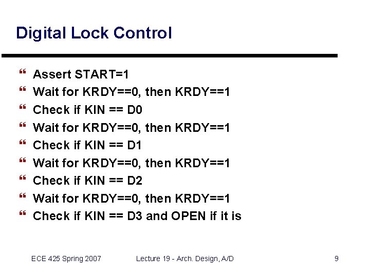
Digital Lock Control } } } } } Assert START=1 Wait for KRDY==0, then KRDY==1 Check if KIN == D 0 Wait for KRDY==0, then KRDY==1 Check if KIN == D 1 Wait for KRDY==0, then KRDY==1 Check if KIN == D 2 Wait for KRDY==0, then KRDY==1 Check if KIN == D 3 and OPEN if it is ECE 425 Spring 2007 Lecture 19 - Arch. Design, A/D 9

Digital Lock Control - State Diagram NOTE: Outputs are listed in the following order: S 1 S 0 START OPEN ECE 425 Spring 2007 Lecture 19 - Arch. Design, A/D 10

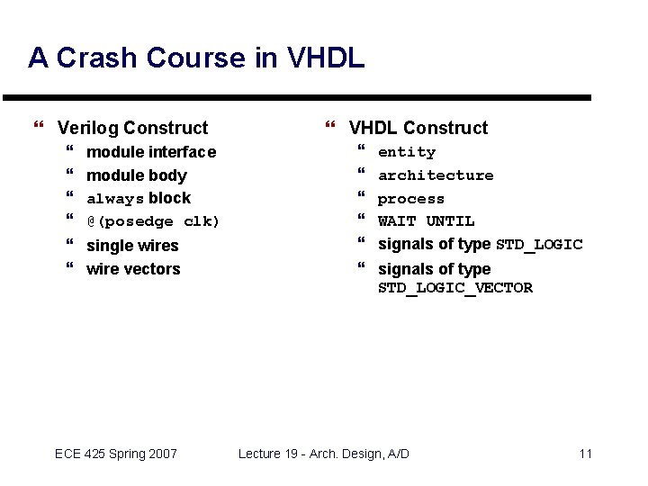
A Crash Course in VHDL } Verilog Construct } } } module interface module body always block @(posedge clk) single wires wire vectors ECE 425 Spring 2007 } VHDL Construct } } } entity architecture process WAIT UNTIL signals of type STD_LOGIC_VECTOR Lecture 19 - Arch. Design, A/D 11

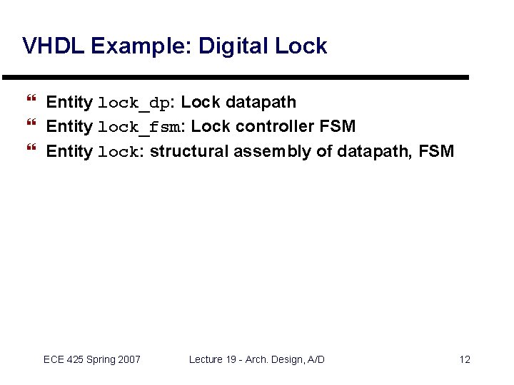
VHDL Example: Digital Lock } Entity lock_dp: Lock datapath } Entity lock_fsm: Lock controller FSM } Entity lock: structural assembly of datapath, FSM ECE 425 Spring 2007 Lecture 19 - Arch. Design, A/D 12

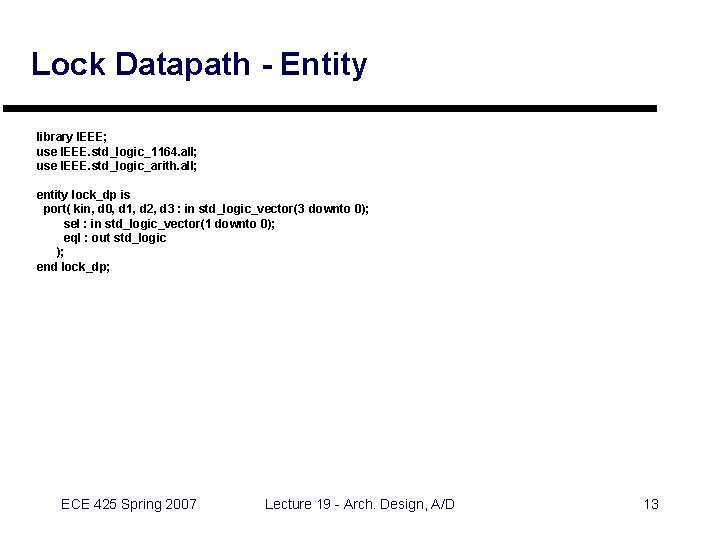
Lock Datapath - Entity library IEEE; use IEEE. std_logic_1164. all; use IEEE. std_logic_arith. all; entity lock_dp is port( kin, d 0, d 1, d 2, d 3 : in std_logic_vector(3 downto 0); sel : in std_logic_vector(1 downto 0); eql : out std_logic ); end lock_dp; ECE 425 Spring 2007 Lecture 19 - Arch. Design, A/D 13

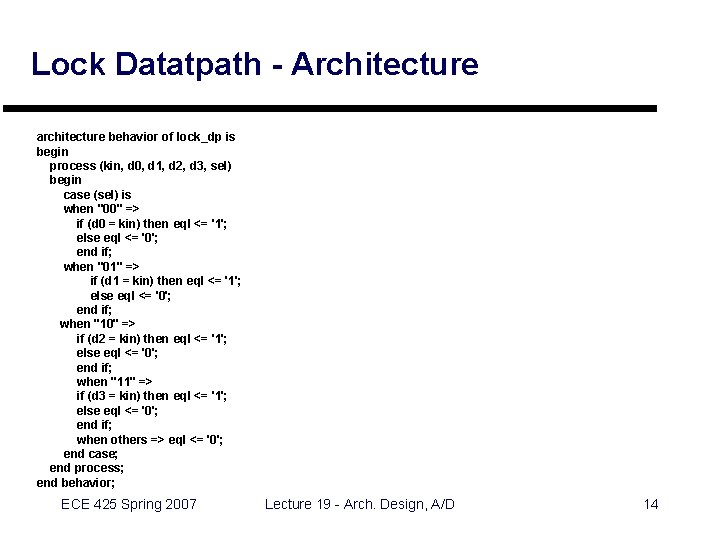
Lock Datatpath - Architecture architecture behavior of lock_dp is begin process (kin, d 0, d 1, d 2, d 3, sel) begin case (sel) is when "00" => if (d 0 = kin) then eql <= '1'; else eql <= '0'; end if; when "01" => if (d 1 = kin) then eql <= '1'; else eql <= '0'; end if; when "10" => if (d 2 = kin) then eql <= '1'; else eql <= '0'; end if; when "11" => if (d 3 = kin) then eql <= '1'; else eql <= '0'; end if; when others => eql <= '0'; end case; end process; end behavior; ECE 425 Spring 2007 Lecture 19 - Arch. Design, A/D 14

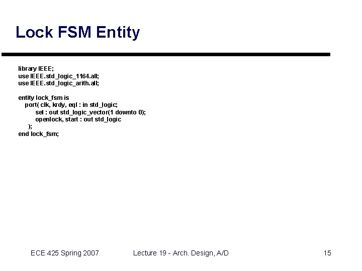
Lock FSM Entity library IEEE; use IEEE. std_logic_1164. all; use IEEE. std_logic_arith. all; entity lock_fsm is port( clk, krdy, eql : in std_logic; sel : out std_logic_vector(1 downto 0); openlock, start : out std_logic ); end lock_fsm; ECE 425 Spring 2007 Lecture 19 - Arch. Design, A/D 15

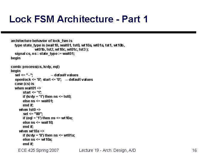
Lock FSM Architecture - Part 1 architecture behavior of lock_fsm is type state_type is (wait 10, wait 01, tst 0, wt 10 a, wt 01 a, tst 1, wt 10 b, wt 01 b, tst 2, wt 10 c, wt 01 c, tst 3 ); signal cs, ns : state_type : = wait 01; begin comb: process(cs, krdy, eql) begin sel <= "--"; -- default values openlock <= '0'; start <= '0'; -- default values case (cs) is when wait 01 => start <= '1'; if (krdy = '1') then ns <= tst 0; else ns <= wait 01; end if; when tst 0 => sel <= "00"; if (eql = '1') then ns <= wt 10 a; else ns <= wait 10; end if; when wt 10 a => if (krdy = '0') then ns <= wt 01 a; else ns <= wt 10 a; end if; ECE 425 Spring 2007 Lecture 19 - Arch. Design, A/D 16

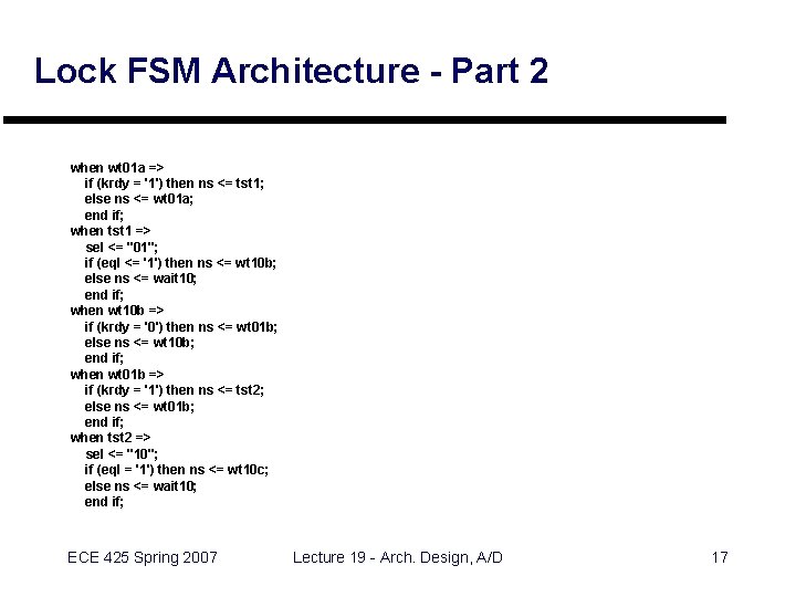
Lock FSM Architecture - Part 2 when wt 01 a => if (krdy = '1') then ns <= tst 1; else ns <= wt 01 a; end if; when tst 1 => sel <= "01"; if (eql <= '1') then ns <= wt 10 b; else ns <= wait 10; end if; when wt 10 b => if (krdy = '0') then ns <= wt 01 b; else ns <= wt 10 b; end if; when wt 01 b => if (krdy = '1') then ns <= tst 2; else ns <= wt 01 b; end if; when tst 2 => sel <= "10"; if (eql = '1') then ns <= wt 10 c; else ns <= wait 10; end if; ECE 425 Spring 2007 Lecture 19 - Arch. Design, A/D 17

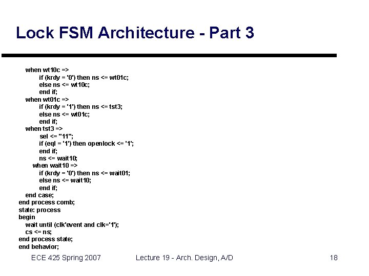
Lock FSM Architecture - Part 3 when wt 10 c => if (krdy = '0') then ns <= wt 01 c; else ns <= wt 10 c; end if; when wt 01 c => if (krdy = '1') then ns <= tst 3; else ns <= wt 01 c; end if; when tst 3 => sel <= "11"; if (eql = '1') then openlock <= '1'; end if; ns <= wait 10; when wait 10 => if (krdy = '0') then ns <= wait 01; else ns <= wait 10; end if; end case; end process comb; state: process begin wait until (clk'event and clk='1'); cs <= ns; end process state; end behavior; ECE 425 Spring 2007 Lecture 19 - Arch. Design, A/D 18

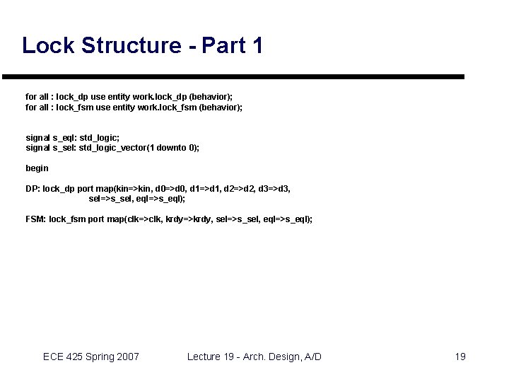
Lock Structure - Part 1 for all : lock_dp use entity work. lock_dp (behavior); for all : lock_fsm use entity work. lock_fsm (behavior); signal s_eql: std_logic; signal s_sel: std_logic_vector(1 downto 0); begin DP: lock_dp port map(kin=>kin, d 0=>d 0, d 1=>d 1, d 2=>d 2, d 3=>d 3, sel=>s_sel, eql=>s_eql); FSM: lock_fsm port map(clk=>clk, krdy=>krdy, sel=>s_sel, eql=>s_eql); ECE 425 Spring 2007 Lecture 19 - Arch. Design, A/D 19

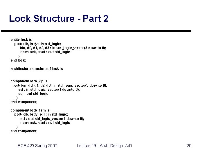
Lock Structure - Part 2 entity lock is port( clk, krdy : in std_logic; kin, d 0, d 1, d 2, d 3 : in std_logic_vector(3 downto 0); openlock, start : out std_logic ); end lock; architecture structure of lock is component lock_dp is port( kin, d 0, d 1, d 2, d 3 : in std_logic_vector(3 downto 0); sel : in std_logic_vector(1 downto 0); eql : out std_logic ); end component; component lock_fsm is port( clk, krdy, eql : in std_logic; sel : out std_logic_vector(1 downto 0); openlock, start : out std_logic ); end component; ECE 425 Spring 2007 Lecture 19 - Arch. Design, A/D 20

A/D Conversion } Basic Circuit Structure ECE 425 Spring 2007 Lecture 19 - Arch. Design, A/D 21

A/D Conversion - Naïve Approach ECE 425 Spring 2007 Lecture 19 - Arch. Design, A/D 22

A/D Using Successive Approximation ECE 425 Spring 2007 Lecture 19 - Arch. Design, A/D 23

A Possible SAR Design ECE 425 Spring 2007 Lecture 19 - Arch. Design, A/D 24

SAR FSM State Diagram ECE 425 Spring 2007 Lecture 19 - Arch. Design, A/D 25

How do we make a Comparator? } One way: use a high-gain differential amplifier } Example Designs From: P. Geiger, P. Allen, and N. Strader, VLSI Techniques for Analog and Digital Circuits Mc. Graw-Hill, 1990 • Two-stage comparator: Fig. 6. 6 -7, p. 505 ECE 425 Spring 2007 Lecture 19 - Arch. Design, A/D 26

Alternative Approach: Auto-Centering Comparator } ø 1, ø 2 - Non-overlapping two-phase clocks ECE 425 Spring 2007 Lecture 19 - Arch. Design, A/D 27

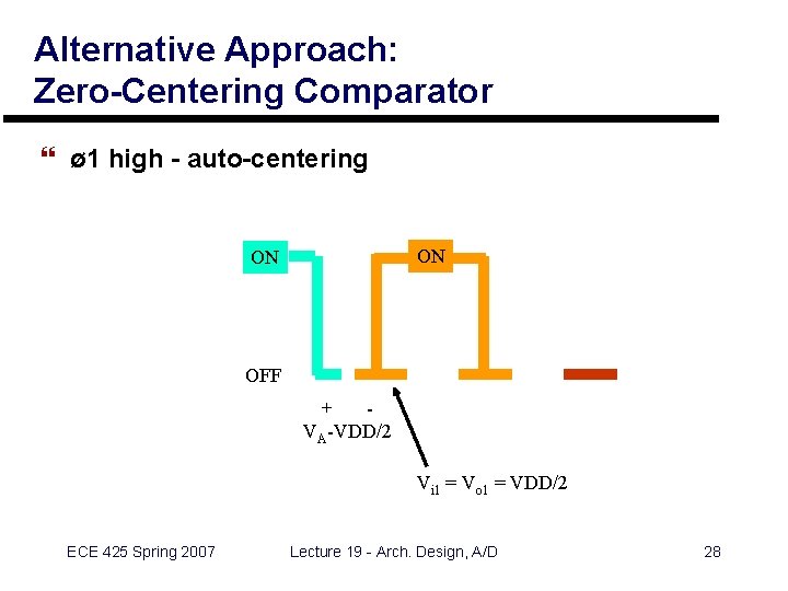
Alternative Approach: Zero-Centering Comparator } ø 1 high - auto-centering ON ON OFF + VA-VDD/2 Vi 1 = Vo 1 = VDD/2 ECE 425 Spring 2007 Lecture 19 - Arch. Design, A/D 28

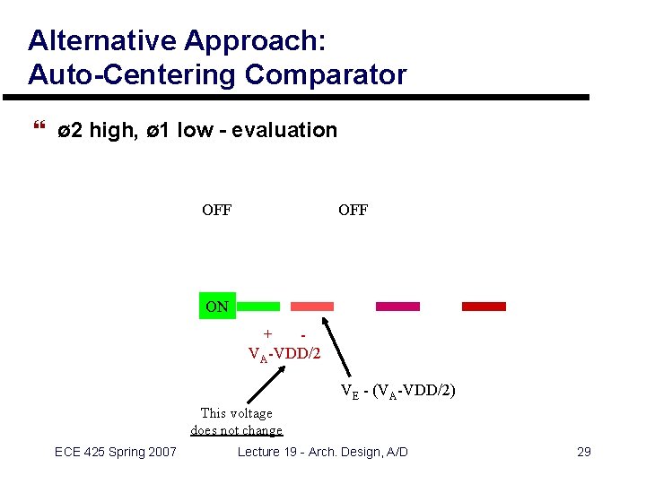
Alternative Approach: Auto-Centering Comparator } ø 2 high, ø 1 low - evaluation OFF ON + VA-VDD/2 VE - (VA-VDD/2) This voltage does not change ECE 425 Spring 2007 Lecture 19 - Arch. Design, A/D 29

Preliminary Layout Auto-Centering Comparator ECE 425 Spring 2007 Lecture 19 - Arch. Design, A/D 30

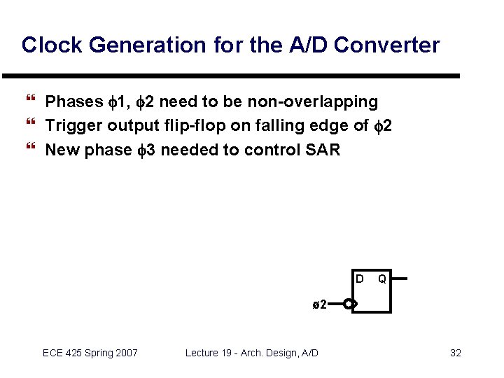
Additional Issues: Auto-Centering Comparator } Isolating comparator output during auto-centering } VDD/2 values can propagate and cause problems, so } add a flip-flop to isolate output from other logic } Generating clocks: } non-overlapping ø 1, ø 2 and ø 1 bar, ø 2 bar } generating clock for SAR ECE 425 Spring 2007 Lecture 19 - Arch. Design, A/D 31

Clock Generation for the A/D Converter } Phases f 1, f 2 need to be non-overlapping } Trigger output flip-flop on falling edge of f 2 } New phase f 3 needed to control SAR D Q ø 2 ECE 425 Spring 2007 Lecture 19 - Arch. Design, A/D 32

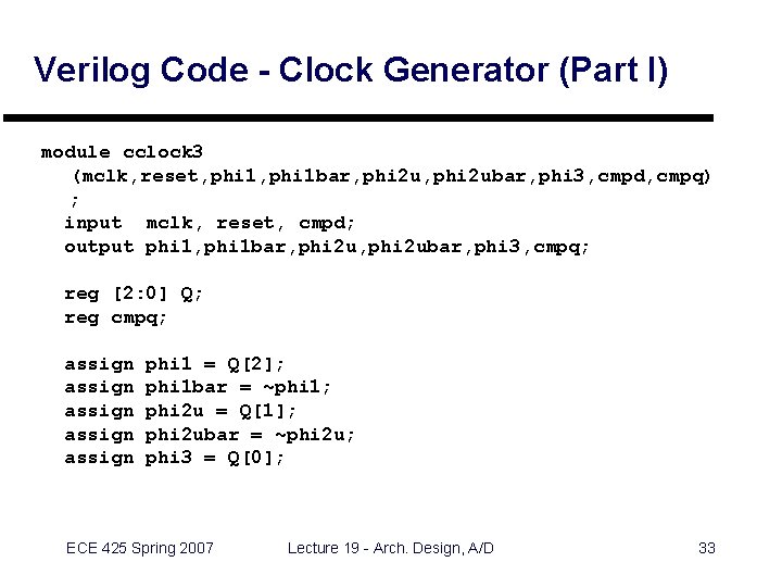
Verilog Code - Clock Generator (Part I) module cclock 3 (mclk, reset, phi 1 bar, phi 2 ubar, phi 3, cmpd, cmpq) ; input mclk, reset, cmpd; output phi 1, phi 1 bar, phi 2 ubar, phi 3, cmpq; reg [2: 0] Q; reg cmpq; assign assign phi 1 = Q[2]; phi 1 bar = ~phi 1; phi 2 u = Q[1]; phi 2 ubar = ~phi 2 u; phi 3 = Q[0]; ECE 425 Spring 2007 Lecture 19 - Arch. Design, A/D 33

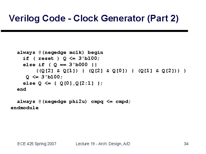
Verilog Code - Clock Generator (Part 2) always @(negedge mclk) begin if ( reset ) Q <= 3'b 100; else if ( Q == 3'b 000 || ((Q[2] & Q[1]) | (Q[2] & Q[0]) | (Q[1] & Q[2])) ) Q <= 3'b 100; else Q <= { Q[0], Q[2: 1] }; end always @(negedge phi 2 u) cmpq <= cmpd; endmodule ECE 425 Spring 2007 Lecture 19 - Arch. Design, A/D 34

Synthesized Layout - Clock Generator ECE 425 Spring 2007 Lecture 19 - Arch. Design, A/D 35

Overall Layout - Comparator Block ECE 425 Spring 2007 Lecture 19 - Arch. Design, A/D 36

More about Comparator cell } Using the cell } Location of cells: /home/nestorj/compare/*. mag } Top-level cell: comparator } Connections: } } MCLK- master clock from input pin phi 3 - clock for your SAR VI, VE - analog inputs GT - digital output ECE 425 Spring 2007 Lecture 19 - Arch. Design, A/D 37

Controlling sv 2 mag } Controlling rows in layout: } sv 2 mag -wolfeflags -r n } Controlling pin placment } create a file “module. pins” for db file “module. db” } Example: file “cclock 3. pins” phi 1 bar phi 1 phi 2 bar cmpd cmpq phi 3 mclk reset top 0. 01 top 0. 02 top 0. 13 top 0. 14 top 0. 2 right 0. 9 right 0. 8 bot 0. 45 bot 0. 55 ECE 425 Spring 2007 Lecture 19 - Arch. Design, A/D 38

Project Assignment } Build Successive Approximation A/D using } DAC from Labs 5 -7 } Comparator discussed here } Successive-approximation circuit with added features: • Include scan logic with extra pins TEST, SCAN_IN, SCAN_OUT • Include hardware to record the maximum converted value since the last reset } Combine to form one half a MOSIS “tiny chip” } Simulate complete design in PSpice ECE 425 Spring 2007 Lecture 19 - Arch. Design, A/D 39

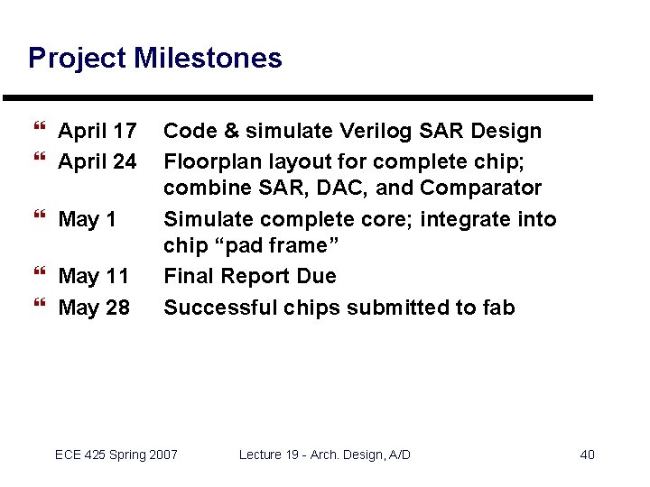
Project Milestones } April 17 } April 24 } May 11 } May 28 Code & simulate Verilog SAR Design Floorplan layout for complete chip; combine SAR, DAC, and Comparator Simulate complete core; integrate into chip “pad frame” Final Report Due Successful chips submitted to fab ECE 425 Spring 2007 Lecture 19 - Arch. Design, A/D 40

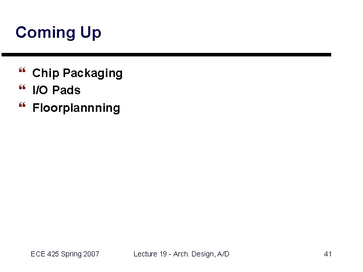
Coming Up } Chip Packaging } I/O Pads } Floorplannning ECE 425 Spring 2007 Lecture 19 - Arch. Design, A/D 41