ECE 425 VLSI Circuit Design Lecture 17 Sequential
- Slides: 38

ECE 425 - VLSI Circuit Design Lecture 17 - Sequential Logic Timing, Testing Spring 2007 Prof. John Nestor ECE Department Lafayette College Easton, Pennsylvania 18042 nestorj@lafayette. edu ECE 425 Spring 2007 Lecture 17 - Seq. Logic (cont'd) 1

Announcements } Reading } Book: 5. 5 -5. 7, 8. 1 -8. 4 } Verilog Handout: Section 5 ECE 425 Spring 2007 Lecture 17 - Seq. Logic (cont'd) 2

Where We Are } Last Time: } Sequential Circuit Timing (intro) } Today: } Sequential Circuit Timing } Sequential Circuit Testing ECE 425 Spring 2007 Lecture 17 - Seq. Logic (cont'd) 3

Sequential Logic - General Structure } State changes on each clock cycle } Next state is function of current state, inputs } Some definitions } Moore machine: output function of current state only } Mealy machine: output depends on current state, inputs ECE 425 Spring 2007 Lecture 17 - Seq. Logic (cont'd) 4

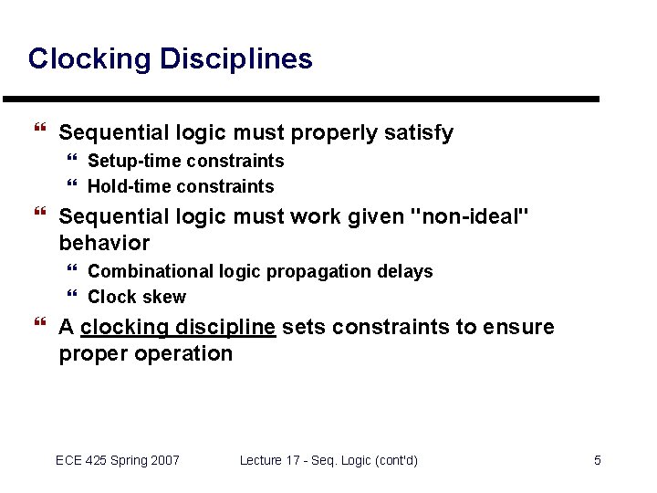
Clocking Disciplines } Sequential logic must properly satisfy } Setup-time constraints } Hold-time constraints } Sequential logic must work given "non-ideal" behavior } Combinational logic propagation delays } Clock skew } A clocking discipline sets constraints to ensure properation ECE 425 Spring 2007 Lecture 17 - Seq. Logic (cont'd) 5

Clocking Disciplines (cont’d) } Basic rules: } Clocking rule 1: "Combinational logic gates cannot be connected in a cycle" } Clocking rule 2: "All components must have bounded delay" ECE 425 Spring 2007 Lecture 17 - Seq. Logic (cont'd) 6

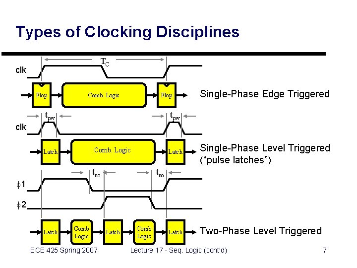
Types of Clocking Disciplines TC clk Flop Comb. Logic Flop tpw Single-Phase Edge Triggered tpw clk Comb. Logic Latch tno Latch Single-Phase Level Triggered (“pulse latches”) Latch Two-Phase Level Triggered tno f 1 f 2 Latch Comb Logic ECE 425 Spring 2007 Latch Comb Logic Lecture 17 - Seq. Logic (cont'd) 7

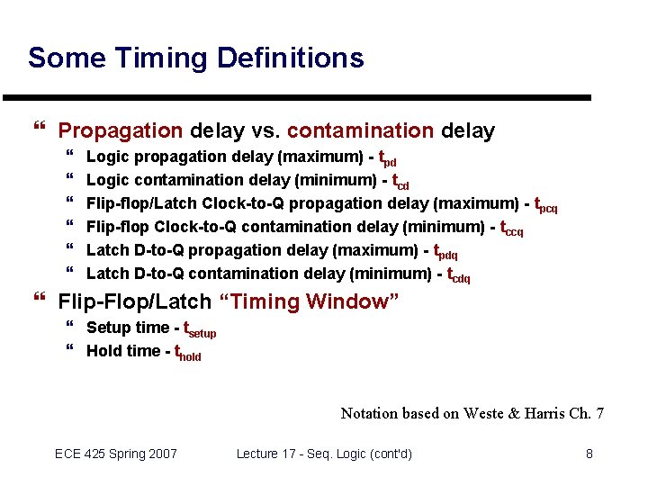
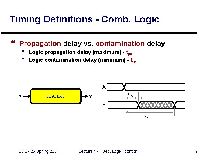
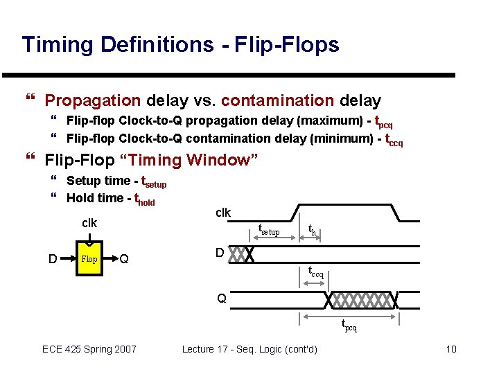
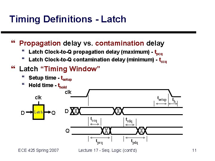
Some Timing Definitions } Propagation delay vs. contamination delay } } } Logic propagation delay (maximum) - tpd Logic contamination delay (minimum) - tcd Flip-flop/Latch Clock-to-Q propagation delay (maximum) - tpcq Flip-flop Clock-to-Q contamination delay (minimum) - tccq Latch D-to-Q propagation delay (maximum) - tpdq Latch D-to-Q contamination delay (minimum) - tcdq } Flip-Flop/Latch “Timing Window” } Setup time - tsetup } Hold time - thold Notation based on Weste & Harris Ch. 7 ECE 425 Spring 2007 Lecture 17 - Seq. Logic (cont'd) 8

Timing Definitions - Comb. Logic } Propagation delay vs. contamination delay } Logic propagation delay (maximum) - tpd } Logic contamination delay (minimum) - tcd A A Comb. Logic tcd Y Y tpd ECE 425 Spring 2007 Lecture 17 - Seq. Logic (cont'd) 9

Timing Definitions - Flip-Flops } Propagation delay vs. contamination delay } Flip-flop Clock-to-Q propagation delay (maximum) - tpcq } Flip-flop Clock-to-Q contamination delay (minimum) - tccq } Flip-Flop “Timing Window” } Setup time - tsetup } Hold time - thold clk D Flop clk tsetup Q th D tccq Q tpcq ECE 425 Spring 2007 Lecture 17 - Seq. Logic (cont'd) 10

Timing Definitions - Latch } Propagation delay vs. contamination delay } Latch Clock-to-Q propagation delay (maximum) - tpcq } Latch Clock-to-Q contamination delay (minimum) - tccq } Latch “Timing Window” } Setup time - tsetup } Hold time - thold clk D Latch Q tsetup th D tccq tcdq Q tpcq ECE 425 Spring 2007 tpdq Lecture 17 - Seq. Logic (cont'd) 11

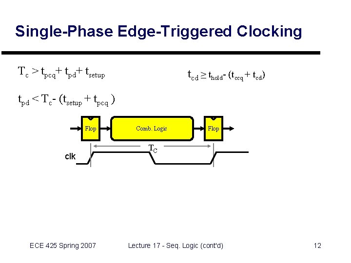
Single-Phase Edge-Triggered Clocking Tc > tpcq+ tpd+ tsetup tcd ≥ thold- (tccq + tcd) tpd < Tc- (tsetup + tpcq ) Flop clk ECE 425 Spring 2007 Comb. Logic Flop TC Lecture 17 - Seq. Logic (cont'd) 12

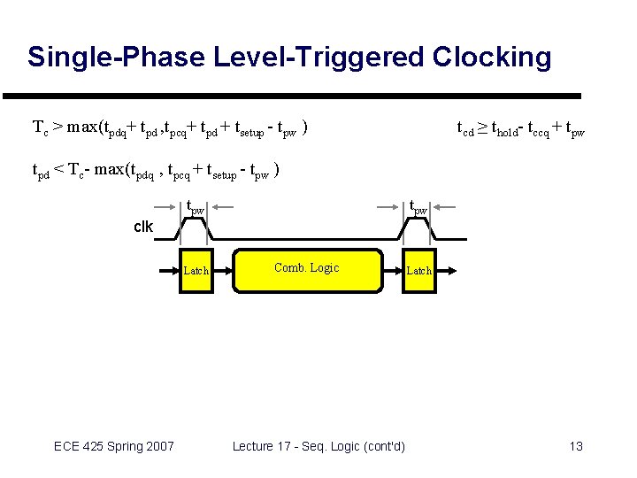
Single-Phase Level-Triggered Clocking Tc > max(tpdq+ tpd , tpcq+ tpd + tsetup - tpw ) tcd ≥ thold- tccq + tpw tpd < Tc- max(tpdq , tpcq + tsetup - tpw ) tpw clk Latch ECE 425 Spring 2007 Comb. Logic Lecture 17 - Seq. Logic (cont'd) Latch 13

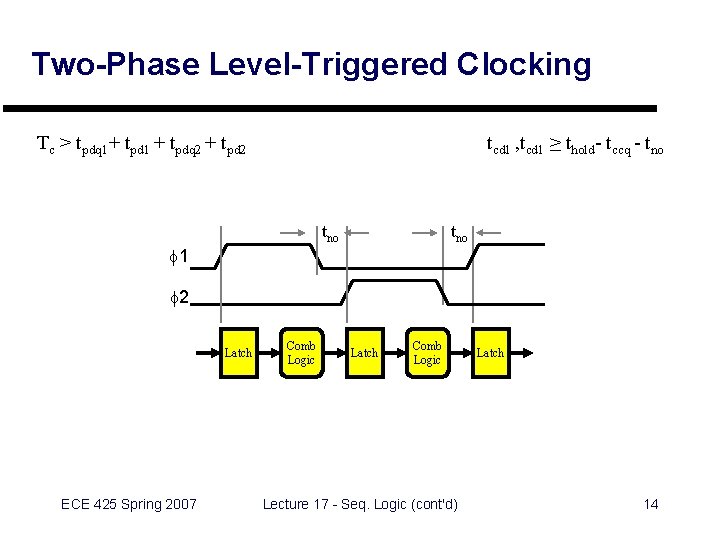
Two-Phase Level-Triggered Clocking Tc > tpdq 1+ tpd 1 + tpdq 2 + tpd 2 tcd 1 , tcd 1 ≥ thold- tccq - tno tno f 1 f 2 Latch ECE 425 Spring 2007 Comb Logic Latch Comb Logic Lecture 17 - Seq. Logic (cont'd) Latch 14

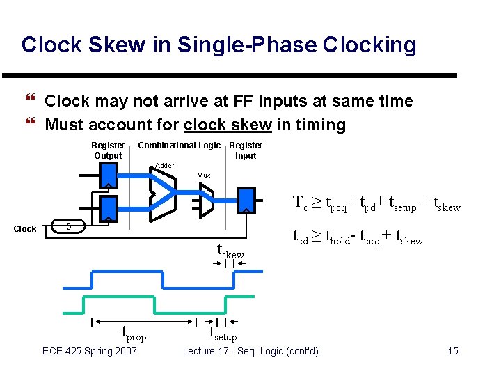
Clock Skew in Single-Phase Clocking } Clock may not arrive at FF inputs at same time } Must account for clock skew in timing Register Output Combinational Logic Register Input Adder Mux Tc ≥ tpcq+ tpd+ tsetup + tskew Clock d tskew tprop ECE 425 Spring 2007 tcd ≥ thold- tccq + tskew tsetup Lecture 17 - Seq. Logic (cont'd) 15

More About Two-phase clocking } Break logic into two sections separated by latches } Use non-overlapping clocks ø 1, ø 2 ECE 425 Spring 2007 Lecture 17 - Seq. Logic (cont'd) 16

Rules for reliable 2 phase design } Every cycle must be broken by both ø 1 and ø 2 latches } Latch inputs must be stable during active phase (sø 1, sø 2) } See Section 5. 3. 2 for more details ECE 425 Spring 2007 Lecture 17 - Seq. Logic (cont'd) 17

Two-phase example - Dynamic Shift Reg. } Basic circuit - one stage } Operation - p. 271 ECE 425 Spring 2007 Lecture 17 - Seq. Logic (cont'd) 18

Two-phase example - Dynamic Shift Reg. } Hierarchical Sticks Diagram - Multiple Phases } Tiling horizontally adds to length of shift register } Tiling vertically adds to width of shift register ECE 425 Spring 2007 Lecture 17 - Seq. Logic (cont'd) 19

Qualified clocks } Logical "AND" of enable signal, clock phase } Application: recirculating latch } Drawback: extra clock skew (unless generated carefully) ECE 425 Spring 2007 Lecture 17 - Seq. Logic (cont'd) 20

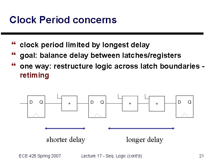
Clock Period concerns } clock period limited by longest delay } goal: balance delay between latches/registers } one way: restructure logic across latch boundaries retiming shorter delay ECE 425 Spring 2007 longer delay Lecture 17 - Seq. Logic (cont'd) 21

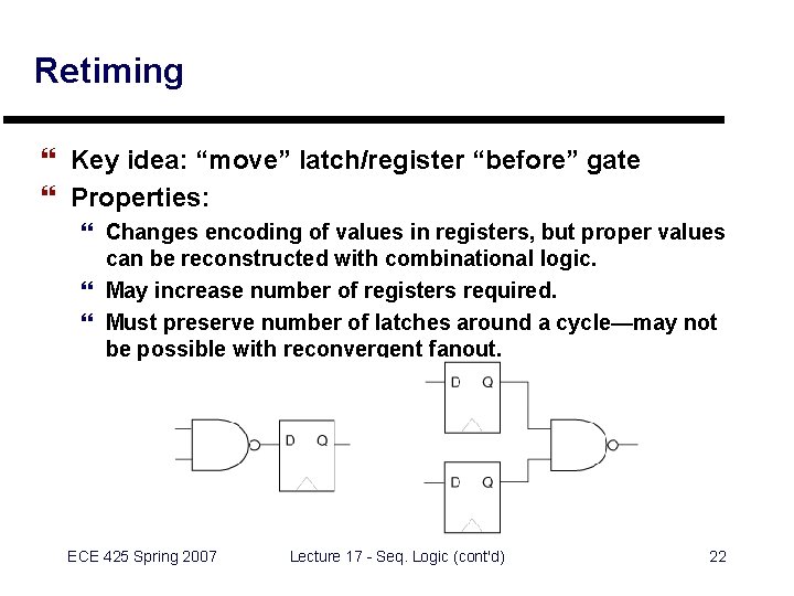
Retiming } Key idea: “move” latch/register “before” gate } Properties: } Changes encoding of values in registers, but proper values can be reconstructed with combinational logic. } May increase number of registers required. } Must preserve number of latches around a cycle—may not be possible with reconvergent fanout. ECE 425 Spring 2007 Lecture 17 - Seq. Logic (cont'd) 22

Two-phase clock generation } It is essential that clock phases be non-overlapping } Generation circuit: Cross-coupled NOR "latch" ECE 425 Spring 2007 Lecture 17 - Seq. Logic (cont'd) 23

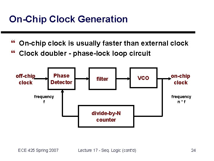
On-Chip Clock Generation } On-chip clock is usually faster than external clock } Clock doubler - phase-lock loop circuit off-chip clock Phase Detector filter frequency f VCO on-chip clock frequency n*f divide-by-N counter ECE 425 Spring 2007 Lecture 17 - Seq. Logic (cont'd) 24

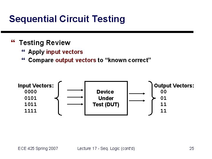
Sequential Circuit Testing } Testing Review } Apply input vectors } Compare output vectors to “known correct” Input Vectors: 0000 0101 1011 1111 ECE 425 Spring 2007 Device Under Test (DUT) Lecture 17 - Seq. Logic (cont'd) Output Vectors: 00 01 11 11 25

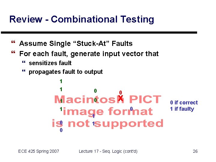
Review - Combinational Testing } Assume Single “Stuck-At” Faults } For each fault, generate input vector that } sensitizes fault } propagates fault to output 1 1 0 0 ECE 425 Spring 2007 0 0 if correct 1 if faulty 1 1 Lecture 17 - Seq. Logic (cont'd) 26

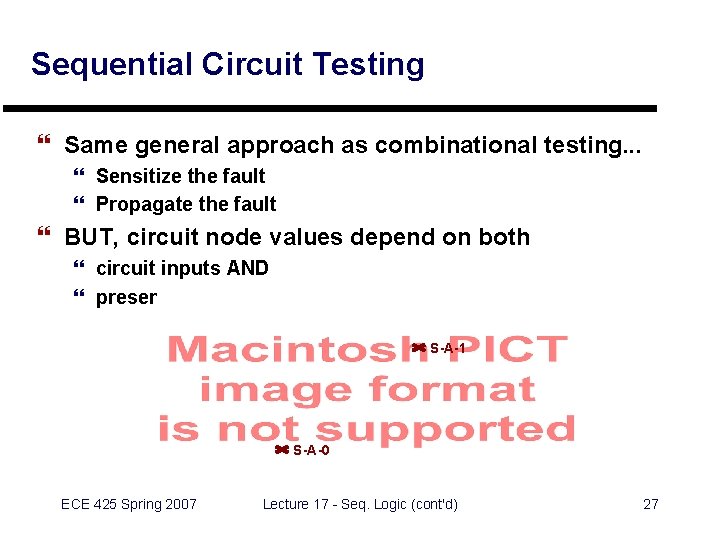
Sequential Circuit Testing } Same general approach as combinational testing. . . } Sensitize the fault } Propagate the fault } BUT, circuit node values depend on both } circuit inputs AND } present state S-A-1 S-A-0 ECE 425 Spring 2007 Lecture 17 - Seq. Logic (cont'd) 27

Sequential Testing Approach } Spread testing over multiple clock cycles } Set flip-flops to proper values to sensitize fault } Set flip-flops to proper value to propagate fault } Sequential circuit testing is hard! } May not be able to sensitize all faults } May not be able to propagate all faults ECE 425 Spring 2007 Lecture 17 - Seq. Logic (cont'd) 28

Sequential Test Example } Identify a S-A-1 fault on node N 1 } Recall testing steps } Sensitize fault } Propagate to output ECE 425 Spring 2007 Lecture 17 - Seq. Logic (cont'd) 29

Three Clock Cycles Needed } Sensitize fault } Make Q 2 = 0 (D=0, } E=0 on 1 st clock) } Set C=0 on 2 nd clock } Propagate fault } N 1 to Q 1(Set B=0) } Q 1 to OUT } (A=1 on 3 rd clock) ECE 425 Spring 2007 Lecture 17 - Seq. Logic (cont'd) 30

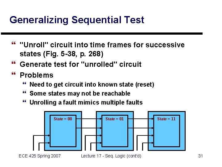
Generalizing Sequential Test } "Unroll" circuit into time frames for successive states (Fig. 5 -38, p. 268) } Generate test for "unrolled" circuit } Problems } Need to get circuit into known state (reset) } Some states may not be reachable } Unrolling a fault mimics multiple faults State = 00 ECE 425 Spring 2007 State = 01 Lecture 17 - Seq. Logic (cont'd) State = 11 31

Design for Test } Goal: make sequential test easier } General approach: provide a different way to set, read flip-flops - scan design } Scan design key ideas } Alter flip-flop / latch design to read second input during test mode } Thread second inputs into a large "shift register" } Connect test input, output, and mode control to chip pins } Use test mode to set, read flip-flops during testing ECE 425 Spring 2007 Lecture 17 - Seq. Logic (cont'd) 32

Scan Design - General Structure ECE 425 Spring 2007 Lecture 17 - Seq. Logic (cont'd) 33

Using Scan Design } Shift in to set FF values } Shift out to read FF values } Scan variations } Full scan - require scan in all flip-flops } Partial scan - require scan in some flip-flops } Boundary scan - use scan for block I/Os (often used in board-level test) ECE 425 Spring 2007 Lecture 17 - Seq. Logic (cont'd) 34

Built-In Self Test (BIST) } Goal: provide limited testing within the chip itself } Typical approach: use Linear Feedback Shift Register (LFSR) } Structure: shift register with exclusive-OR feedback } "Pseudo-random" state sequence ECE 425 Spring 2007 Lecture 17 - Seq. Logic (cont'd) 35

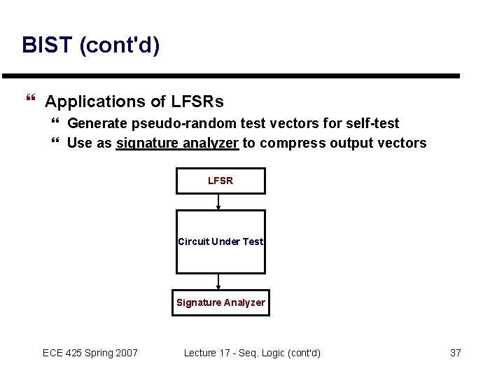
BIST (cont'd) } Applications of LFSRs } Generate pseudo-random test vectors for self-test } Use as signature analyzer to compress output vectors ECE 425 Spring 2007 Lecture 17 - Seq. Logic (cont'd) 36

BIST (cont'd) } Applications of LFSRs } Generate pseudo-random test vectors for self-test } Use as signature analyzer to compress output vectors LFSR Circuit Under Test Signature Analyzer ECE 425 Spring 2007 Lecture 17 - Seq. Logic (cont'd) 37

Coming Up } Sequential Design in Verilog } Architecture Design } Chip-Level Design ECE 425 Spring 2007 Lecture 17 - Seq. Logic (cont'd) 38