
ECE 425 VLSI Circuit Design Lecture 16 Sequential










- Slides: 27
ECE 425 - VLSI Circuit Design Lecture 16 - Sequential Logic Spring 2007 Prof. John Nestor ECE Department Lafayette College Easton, Pennsylvania 18042 nestorj@lafayette. edu ECE 425 Spring 2007 Lecture 16 - Seq. Logic 1
Announcements } Reading } Book: 5. 1 -5. 4 } Verilog Handout: 5. 1 -5. 3, 5. 6 ECE 425 Spring 2007 Lecture 16 - Seq. Logic 2
Where we are } Last Time: } Combinational Logic / Verilog ASIC Design } Today: } Sequential Logic ECE 425 Spring 2007 Lecture 16 - Seq. Logic 3
Review: Combinational vs. Sequential Logic } Combinational Logic } Output depends on current input } Sequential Logic } Output depends on current input AND } Output depends on stored state next state current state ECE 425 Spring 2007 Lecture 16 - Seq. Logic 4
Review: Memory Elements } Latch - "transparent" while enabled (level-sensitive) } Flip-flops - transfer data on active edge ECE 425 Spring 2007 Lecture 16 - Seq. Logic 5
Review: Memory Element Timing } Setup time tsu - time D must be stable before data transfer } Hold time tsu - time D must be stable after transfer ECE 425 Spring 2007 Lecture 16 - Seq. Logic 6
Static Storage Elements } Key circuit: cross-coupled inverters (or NOR gates) } Static storage - feedback preserves value while power is on } Avoided in CMOS due to large size, delay ECE 425 Spring 2007 Lecture 16 - Seq. Logic 7
Aside: Regenerative Storage Elements } Two stable states } Vo 1=L, Vo 2=H } Vo 1=H, Vo 2=L } One metastable state } Vo 1 = Vo 2 } Ugly characteristic: unbounded delay for recovery from metastable state Graphic source: J. Rabaey, Digital Integrated Circuits, © Prentice-Hall, 1996 ECE 425 Spring 2007 Metastable point Lecture 16 - Seq. Logic 8
Simplest CMOS Latch: Dynamic Latch } When ø=1 (ø'=0) - latch enabled } charge/discharge Cg on inverter input to "load" } output follows input changes "transparent" operation } When ø=0 (ø'=1) - latch disabled } output uses stored value in Cg } must use or rewrite value before charge in Cg decays (~1 ms) ECE 425 Spring 2007 Lecture 16 - Seq. Logic Parasitic Capacitance used for Storage 9
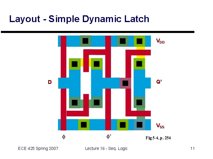
Layout - Simple Dynamic Latch } Stick diagram } p-transistors in top } n-transistors in bottom } vertical ø, ø' lines allow creation of multiple-bit latches! ECE 425 Spring 2007 Lecture 16 - Seq. Logic 10
Layout - Simple Dynamic Latch VDD Q’ D VSS ECE 425 Spring 2007 ’ Lecture 16 - Seq. Logic Fig 5 -4, p. 254 11
Dynamic Latch Timing } Setup time tsu: time to charge / discharge Cg plus inverter prop delay } Hold time th: "turn-off" time of transmission gate } Result of violating tsu, th window: } Capacitor Cg not fully charged/discharged } Incorrect / Invalid output value ECE 425 Spring 2007 Lecture 16 - Seq. Logic 12
Multiplexed Dynamic Latch } Multiple inputs D 1, D 2 } A, B must never be 1 at same time ECE 425 Spring 2007 Lecture 16 - Seq. Logic 13
Recirculating “Quasi-Static” Latch } Modes of operation: } LD High, ø Low: "transparent" } LD Low, ø Low: "opaque" } ø High: "recirculating" (LD must be Low here!) (q 1) - “Qualified” by 1 } Special considerations: } LD "qualified" by ø 1 } ø 1, ø 2 must not overlap (q 1) } Problem: charge sharing when driving large load (fix: buffering) ECE 425 Spring 2007 Lecture 16 - Seq. Logic 14
Clocked Inverter A Latch Building Block } Combines inverter, transmission gate } Operation } f=1: acts like normal inverter } f=0: high impedance output } f, f' placed closest to output for fast switching between modes ECE 425 Spring 2007 Lecture 16 - Seq. Logic 15
Clocked-Inverter Latch } Operation } f=1 (f'=0): Inverter 1 "on", latch transparent } f=0 (f'=1): Inverter 2 "on", latch; recirculates ECE 425 Spring 2007 Lecture 16 - Seq. Logic 16
Alternative: Regenerative Latch } Omit "clocked" p-transistors } Use feedback to regenerate values + + + f in ECE 425 Spring 2007 out Lecture 16 - Seq. Logic 17
Alternative: Clocked SR Latch } Alternative to "cross-coupled NOR" structure used in bipolar logic families } Fully static } Transistors must be carefully sized (Fig. 5 -12, p. 260) ECE 425 Spring 2007 Lecture 16 - Seq. Logic 18
Flip-Flops } Key difference: flip-flops are non-transparent } Output isolated from input except at clock edge } Types of flip-flops } Master-Slave ("pulse triggered") } Edge-Triggered ECE 425 Spring 2007 Lecture 16 - Seq. Logic 19
Master-Slave Flip-Flops } Master stage: } transparent while ø high } disabled while ø low } Slave stage: } transparent while ø low } transparent while ø high } Q output changes on falling edge of ø ECE 425 Spring 2007 Lecture 16 - Seq. Logic 20
Pseudo-Static Master-Slave FF ECE 425 Spring 2007 Lecture 16 - Seq. Logic 21
Edge-Triggered Flip-Flops } Designed to respond only on clock edge } Positive Edge-Triggered: Rising Edge } Negative Edge-Triggered: Falling Edge } Approaches } Construct from master-slave flip-flop (see below) } Construct from static gates (see ECE 212) Negative Edge-Triggered ECE 425 Spring 2007 Positive Edge-Triggered Lecture 16 - Seq. Logic 22
Dynamic Negative Edge-Triggered FF } Constructed using Clocked Inverters } Not sensitive to overlap (if clock edge rise/fall times "sufficiently small" } Often used for pipelineing latches (more later) ECE 425 Spring 2007 Lecture 16 - Seq. Logic 23
Example: A Standard-Cell NETFF } MSU Standard Cell DFNF 311 - Circuit Diagram ECE 425 Spring 2007 Lecture 16 - Seq. Logic 24
Example: A Standard-Cell NETFF } Transistor Schematic ECE 425 Spring 2007 Lecture 16 - Seq. Logic 25
Example - A Standard-Cell NETFF } MSU Standard cell DFNF 311 - Layout ECE 425 Spring 2007 Lecture 16 - Seq. Logic 26
Coming Up: } Clocking Disciplines } Sequential logic in Verilog HDL } FSM Design ECE 425 Spring 2007 Lecture 16 - Seq. Logic 27