ECE 425 VLSI Circuit Design Lecture 11 Combinational
ECE 425 - VLSI Circuit Design Lecture 11 - Combinational Logic Networks Spring 2007 Prof. John Nestor ECE Department Lafayette College Easton, Pennsylvania 18042 nestorj@lafayette. edu ECE 425 Spring 2007 Lecture 11 - Comb. Networks 1
Announcements } Homework Due Mon. March 5 } Elmore Delay Problem } Reading } 3. 1 -3. 7 (3. 8 optional) } Exam 1: Wed. March 21 (rescheduled) } Talk today: Quantum Information (Hugel 100, 12 pm, free pizza!) ECE 425 Spring 2007 Lecture 11 - Comb. Networks 2
Where we are } Last Time } Body Effect } Techniques for Reducing Power Consumption } Delay in long wires } Today } Combination Logic Networks - Layout } Combinational Logic Networks - Placement & Routing ECE 425 Spring 2007 Lecture 11 - Comb. Networks 3
Combinational Logic Networks (Ch. 4) } } Layouts for logic networks Delay through networks Power consumption in networks Testing ECE 425 Spring 2007 Lecture 11 - Comb. Networks 4
Layout Methods } Goal: design cells to work together } Single-row layouts } Multiple-row layouts ECE 425 Spring 2007 Lecture 11 - Comb. Networks 5
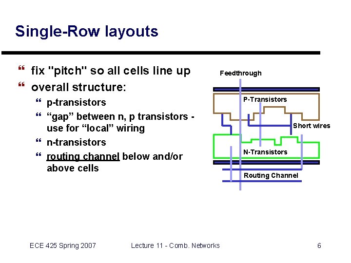
Single-Row layouts } fix "pitch" so all cells line up } overall structure: } p-transistors } “gap” between n, p transistors use for “local” wiring } n-transistors } routing channel below and/or above cells ECE 425 Spring 2007 Lecture 11 - Comb. Networks Feedthrough P-Transistors Short wires N-Transistors Routing Channel 6
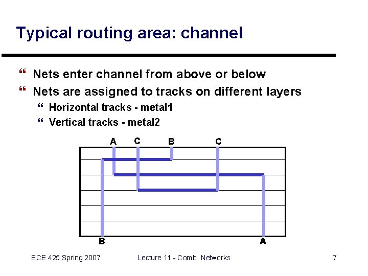
Typical routing area: channel } Nets enter channel from above or below } Nets are assigned to tracks on different layers } Horizontal tracks - metal 1 } Vertical tracks - metal 2 A C B ECE 425 Spring 2007 A Lecture 11 - Comb. Networks 7
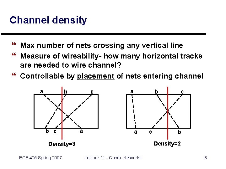
Channel density } Max number of nets crossing any vertical line } Measure of wireability- how many horizontal tracks are needed to wire channel? } Controllable by placement of nets entering channel a c b b c a a a c b Density=2 Density=3 ECE 425 Spring 2007 c b Lecture 11 - Comb. Networks 8
Example: Full adder layout } EXOR sum function (2 EXOR gates) } AND/OR carry function (3 NAND gates) ECE 425 Spring 2007 Lecture 11 - Comb. Networks 9
Example: Full adder layout } Layout method } } Place gates in row draw wires between inputs, outputs measure channel density interchange gates to try to reduce density ECE 425 Spring 2007 Lecture 11 - Comb. Networks 10
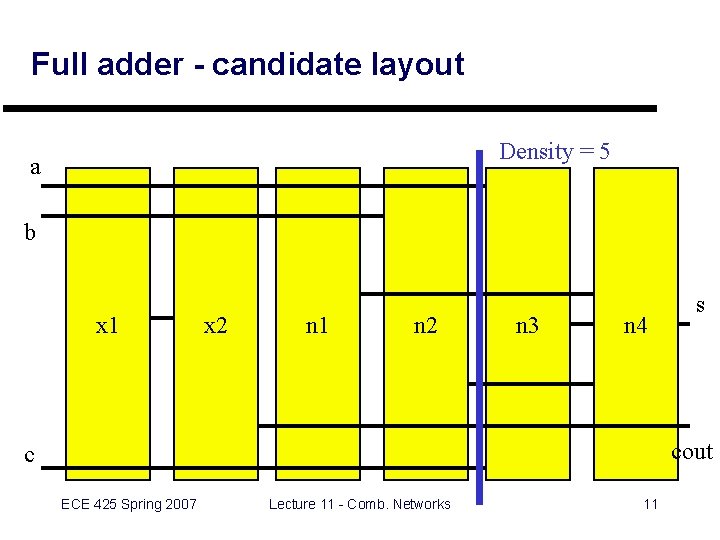
Full adder - candidate layout Density = 5 a b x 1 x 2 n 1 n 2 n 3 n 4 s cout c ECE 425 Spring 2007 Lecture 11 - Comb. Networks 11
Full Adder - Improvement Strategies } Swap pairs of gates. } Doesn’t help here. } Exchange larger groups of cells. } Swapping order of sum and carry groups doesn’t help either. } This seems to be the placement that gives the lowest channel density. } Cell sizes are fixed, so channel height determines area. ECE 425 Spring 2007 Lecture 11 - Comb. Networks 12
Channel Routing The Left Edge Algorithm } Basic algorithm for channel routing } Assumes one horizontal segment per net } Operation: } } } Sort nets by left edge Start with first track Place nets that don't overlap in first track Go to second track Repeat until all nets placed } Demonstration: Java applet http: //foghorn. cadlab. lafayette. edu/cadapplets/Channel. Router. html ECE 425 Spring 2007 Lecture 11 - Comb. Networks 13
Vertical Constraints } Consider the case where: } A terminal “A” at the top of a column AND } A terminal “B” at the bottom of a column? } Must assign A to a horizontal track above B - a vertical constraint ECE 425 Spring 2007 Lecture 11 - Comb. Networks 14
Vertical Constraints (cont'd) } Constraint graph - maps constraint relationships ECE 425 Spring 2007 Lecture 11 - Comb. Networks 15
Vertical constraint cycles } Cycle in graph means constraint can’t be met } Fix by inserting "dogleg" ECE 425 Spring 2007 Lecture 11 - Comb. Networks 16
Maze Routing A Less-Constrained Approach } Treat routing surface as a grid } Mark endpoints of desired connection on grid } Source } Target } Lee Algorithm } Label nodes with distance from source in expanding “wavefront” } Trace back connection by following path of decreasing distance } Maze Router Applet: http: //foghorn. cadlab. lafayette. edu/cadapplets/Maze. Router. html ECE 425 Spring 2007 Lecture 11 - Comb. Networks 17
More about Maze Routing } Down side of maze routing: slow } Faster alternatives: } A* algorithm: use distance from source + estimated distance to target as cost function } Hadlock’s algorithm: use “detour number” as cost function i. e. how many grids “away” from target is a path? } Both faster in best case; same speed in worst case } Applets: http: //foghorn. cadlab. lafayette. edu/cadapplets/AStar. Router. html http: //foghorn. cadlab. lafayette. edu/cadapplets/Hadlock. Router. html ECE 425 Spring 2007 Lecture 11 - Comb. Networks 18
Comparing Routing Algorithms } Left-Edge Algorithm + + - Fast execution time, low memory requirements Useful when thinking about layout problems Constrained routing region (channel) Doesn’t expand well to multiple layers Vertical constraints complicate the problem } Lee Algorithm + + + - Unconstrained routing region (grid) Guaranteed to find a connection if one exists Easily extended for multiple layers Slow execution time, high memory requirements } Real routers use a combination of techniques ECE 425 Spring 2007 Lecture 11 - Comb. Networks 19
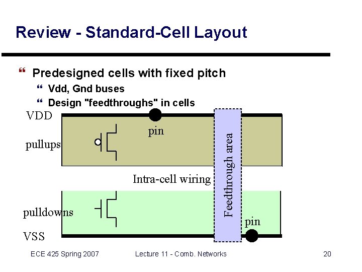
Review - Standard-Cell Layout } Predesigned cells with fixed pitch } Vdd, Gnd buses } Design "feedthroughs" in cells pin pullups Intra-cell wiring pulldowns Feedthrough area VDD pin VSS ECE 425 Spring 2007 Lecture 11 - Comb. Networks 20
Review - Standard-Cell Layout } Layout in multiple rows } Placement • Use an estimate of routing • Try to minimize congestion, wirelength } Routing - two-phase process • Global router - assigns nets to channels • Detailed router - make detailed connections (channel router) } Note impact of layout on delay! ECE 425 Spring 2007 Lecture 11 - Comb. Networks 21
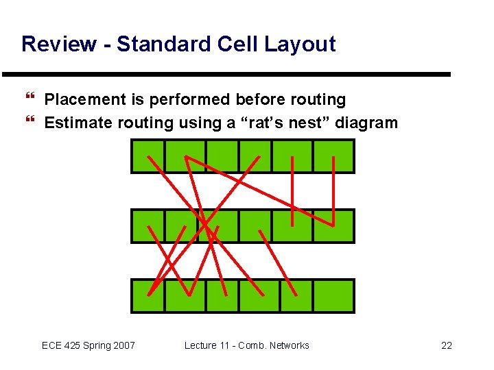
Review - Standard Cell Layout } Placement is performed before routing } Estimate routing using a “rat’s nest” diagram ECE 425 Spring 2007 Lecture 11 - Comb. Networks 22
Coming Up } } Combinational Network Delay Power Issues Testing ASIC Design Using Logic Synthesis ECE 425 Spring 2007 Lecture 11 - Comb. Networks 23
Lab 7 - Verifying the DAC } Modify RPT cell to “mark” resistor for extraction : paint rpoly } Extract circuit & make Spice deck } On Suns: : extract all : ext 2 pspice DAC } On Linux (inside Magic): extract all exttospice cell_name shell sp 2 ps cell_name } Simulate using PSPICE and verify output for all 16 input values (0000 - 1111) ECE 425 Spring 2007 Lecture 11 - Comb. Networks 24
- Slides: 24