ECE 404 PCB Design By Julian Rene Cuellar

ECE 404 PCB Design.

By Julian Rene Cuellar Buritica Guided by Dr. Scott Umbaugh Graduate Program Director Department of Electrical & Computer Engineering Southern Illinois University - Edwardsville

Overview • Introduction – Why PCB? • Materials of PCB • Parts of PCB – Jumpers – Solder Mask – Silkscreen • • • Multilayer PCB Physical Design Issues Design Software Material Required to Design PCB Manual PCB Design PCB Manufacturing Companies

Introduction • Printed Circuit Board • Mechanical support • Electrically connect electronic components using conductive pathways, or traces • PCB populated with electronic components is a printed circuit assembly (PCA)

Why PCB? • Rugged, inexpensive, and can be highly reliable • Faster (due to automation) and consistent in high volume production • Professional(more neater look)

Wire wrapping circuit board

Materials of PCB • Conducting layers are typically made of thin copper foil. • The board is typically coated with a solder mask that is green in color. Other colors that are normally available are blue and red. • Unwanted copper is removed from the substrate after etching leaving only the desired copper traces or pathways

Dielectric PCB Layer • Most common material for PCB is the FR-4 board: – FR stands for Flame Retardant. – Composite material with woven fiberglass cloth with an epoxy resin binder. – Thickness of FR-4 and copper specified separately. – Copper foil thickness in (oz/ft^2), [simply ounce]. • 1 oz/ft^2 copper foil has a thickness of 35 µm. • 1/0 - 1 oz/ft^2 copper one side, with no on the other. • 1/1 - denotes 1 oz/ft^2 copper on both sides.

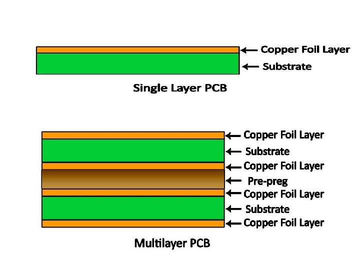
Different Layers of PCB

Parts of a PCB • • • Components Pads Traces Vias Top Metal Layer Bottom Metal Layer

Components • Components are the actual devices used in the circuit. • This includes input/output connections. • I/O ports, including power supply connections, are also important in the PCB design.

Components

Pads • Location that components connect to. • You will solder components to the pads on the PCB. • Pads will connect to traces. • Pads have an inner diameter and outer diameter.

Pads and Trace

Traces • Traces connect pads together. • Traces are essentially the wiring of the PCB. • Equivalent to wire for conducting signals • Traces sometimes connect to vias. • High current traces should be wide. • Signal traces usually narrower than power or ground traces

Vias • Pad with a plated hole connecting traces from one layer of board to other layers. • Attempt to minimize via use in your PCBs. • Some component leads can be used as vias.

Vias 1. Blind Via 2. Buried Via 3. Through hole Via

Top Metal Layer • Most of the components reside on the top layer • Fewer traces on the top layer • Components are soldered to the pads on the top layer of PCB • Higher circuit densities

Bottom Metal Layer • Few components on this layer. • Many traces on this layer. • Most soldering done on this layer.

Jumpers • Often, many signal wires need to exist in too small of a space and must overlap. • Running traces on different PCB layers is an option. • Multilayer PCBs are often expensive. • Solution: Use jumpers

Jumpers

Solder Mask • Protect copper traces on outer layers from corrosion • Areas that shouldn't be soldered may be covered with polymer resist solder mask coating • Designed to keep solder only in certain areas • Prevents solder form binding between conductors and thereby creating short circuits(i. e. hides traces from solder)

Soldering • Wave Soldering- for through hole and SMT • Reflow Soldering- for SMT

Silkscreen • Printing on the solder mask to designate component locations • Readable information about component part numbers and placement. • Helpful in assembling, testing and servicing the circuit board.

Multilayer PCBs • More than a top and bottom layer. • Typically there will be a power plane, ground plane, top layer, and bottom layer. • Sometimes signal layers are added as needed. • Sometimes RF planes made of more expensive materials are added.

Physical Design Issues • • Component Size Heat Dissipation Input and Output Mounting Points

Component Size • Make sure components will actually fit. • This especially applies for circuits that require high component densities. • Some components come in multiple sizes. SMT vs Through Hole • Sometimes you can get tall and narrow caps or short and wide capacitors.

Heat Dissipation-Heat Sinks • Heat sink dissipates heat off the component • Does not remove heat, just moves it • Some components get hot, requiring heat sink • Data sheets specify the size of the heat sink Ø A short circuit may result when two devices share the same heat sink

Mounting Points • PCB needs to be mechanically secured Ø To chassis-consist of metal frame on which the circuit boards and other electronic components are mounted Ø To another PCB/socket on PCB Ø To attachments to a heatsink

Parasitics • High frequency circuits ØSeries Inductance ØShunt Capacitance ØInductive Coupling ØCapacitive Coupling
 • Inductance of")
Series Inductance • Not an issue for low frequency circuits(<10 Mhz) • Inductance of a trace may be significant • Power connections - add shunt capacitor to counter the series inductance of a long trace • Capacitor has a low AC impedance • A 100 n. F capacitor is often used along with a larger capacitor. 100 n. F ceramics have very low impedance at higher frequencies.

Shunt Capacitance • Result of wide wires over a ground plane. • Limits speed of circuits, including digital circuits • Insignificant for low performance circuits • Capacitor from voltage to ground will minimize

Inductive Coupling • Transfer of energy from one circuit component to another through shared magnetic field • Change in current flow through one device induces current flow in other device • Current flow in one trace induces current in another trace ØMinimize the long parallel runs of traces ØRun traces perpendicular to each other

Capacitive Coupling • Transfer of energy in electrical network due to capacitance between circuit nodes • Minimizing long traces on adjacent layers will reduce capacitive coupling • Ground planes are run between the signals that might affect each other.

Routing

Trace connection with Pads

Pre-work • Thoroughly simulate your circuit-make sure the circuit worked in simulations • Thoroughly test the prototype-make sure the circuit worked on the bread board • Have all the data sheets handy for all components • Try various component configurations

Simulations • Important to simulate the circuits before building them • Allow margin for component tolerances • Avoid using precise components. e. g a PWM controller that requires exact 10 V DC to work and will fail if there is 10. 01 V • High performance circuits or SMT devices require PCBs and should be simulated extensively first

Transferring your design to a board • Direct Transfer using marker • "Press-N-Peel" sheets and Variations use of heat • Blender pen • Photolithography use of UV light

Design Software ØProteus Profesional ØCADSoft EAGLE ØPCBWizard ØOr. CAD … Gerber files: Describe the images of a printed circuit board (copper layers, solder mask, legend, etc. ) as well as the drilling and milling data, de facto standard used by industry to describe PCB images

PCB Design

Example Gerber files

Materials Required to make PCB • • Drill machine. Cloth Iron. Laser Printer. Photo paper / Glossy paper. Gloves. Ferric Chloride (Etching solution) PCB board. Black permanent Marker.

Manual PCB design Step 1: Take printout of PCB layout • Using laser printer & glossy paper • Mirror image Step 2: Cutting the copper plate

Steps in PCB design Step 3: Make it smooth • Rub the copper side • Removes top oxide layer and photo resist layer • Sanded surface allow image to stick better

Steps in PCB design Step 4: Printing Design layout to board • Method 1: Iron on glossy paper ( transfers the toner) • Method 2: Circuit by hand (using marker)
 • Iron it")
Steps in PCB design Step 5: Apply heat (Iron it !!) • Iron it image down to copper side • Apply little pressure for 10 -15 min • Iron heat transfer toner to cooper plate CAUTION: Do not directly touch copper plate because it is very hot due to ironing.

Steps in PCB design Step 6: Peeling • Place printed plate in Luke warm water (10 min) • Remove the paper • Use black marker to dark lighted track

Steps in PCB design Step 7: Etching • Dissolve 2 -3 tea spoon ferric chloride in water • Dip PCB in etching solution for 30 min • Fe. Cl 3 reacts with unmasked Cu and removes unwanted Cu • Cu + Fe. Cl 3 = Cu. Cl 3 + Fe
 • Few drops")
Steps in PCB design Step 8: Apply thinner ( Final touch) • Few drops of thinner (acetone or nail polish) on pinch of cotton will remove the remaining toner • Rinse carefully and dry with a clean cloth

Steps in PCB Design Step 9: Drill holes and apply Solder Mask • Apply solder mask area to entire board with the exception of solder pads

Steps in PCB Design Step 10. Solder Coat Apply solder to pads Step 11: Silkscreen Apply white letter marking using screen printing process http: //www. youtube. com/watch? v=Q 6 WJqj. Vle. G 0&feature=related
 • J‐STD‐ 001")
PCB Design/Assembly Standards • IPC-2221 (Generic Standard on Printed Board Design) • J‐STD‐ 001 (Requirements for Soldered Electrical and Electronic Assemblies) • IPC‐A‐ 630 (Standard for Manufacture, Inspection and Testing) • IPC-A-610 (Acceptability/Inspection) • IPC-J-STD-001 (How to build PCB/Meet 610)
 •")
PCB Manufacturing Companies • OSHPARK - https: //oshpark. com/ (2 layer - $5/in^2) • Advance Circuits 4 PCB - https: //www. 4 pcb. com/ • PCB Express - https: //www. expresspcb. com/ (2 layer 2 B$9. 85) • Sunstone Circuits - https: //www. sunstone. com/ • PCBCart - https: //www. pcbcart. com/ • epec Engineered Technologies -

WEBSITES • • http: //www. advancedcircuits. com https: //www. orcad. com/ https: //www. altium. com/ https: //www. labcenter. com/ http: //www. ipc. org/ https: //www. flexiblecircuit. com/products/multi-layerflex/ https: //www. amitroncorp. com/? page_id=49
 1. Go to")
EAGLE Layout editor How to download the software (EAGLE Layout editor) 1. Go to http: //www. cadsoftusa. com 2. Click ‘Freeware’ 3. Click ‘Download’ 4. Find the correct version (Windows/Linux, English) 5. Also download Manual and Tutorial

References • • PCB Design slides by Jakia Afruz www. wikipedia. org www. pcbexpress. com A Practical Guide to high-speed printed circuit board layout
- Slides: 58