ECE 385 Final Review Yikuan Chen 2018 Modified





- Slides: 55

ECE 385 Final Review Yikuan Chen, 2018 Modified by Yanpei Tian 11/10/2018 Modified by Keshav Harisrikanth FA 2019 Modified by Derek Wood, Keshav Harisrikanth FA 2019

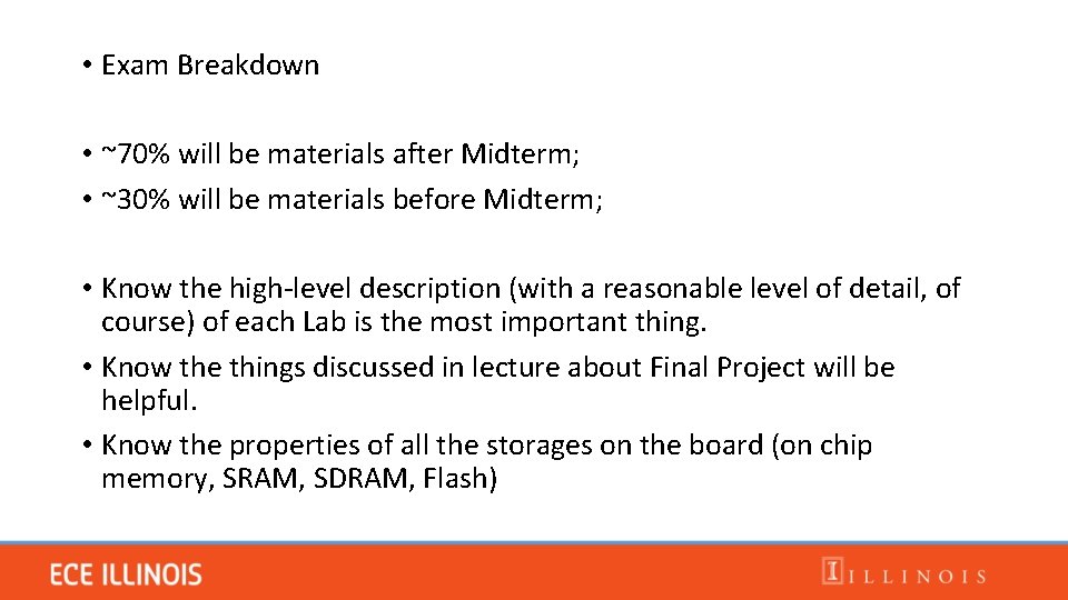
• Exam Breakdown • ~70% will be materials after Midterm; • ~30% will be materials before Midterm; • Know the high-level description (with a reasonable level of detail, of course) of each Lab is the most important thing. • Know the things discussed in lecture about Final Project will be helpful. • Know the properties of all the storages on the board (on chip memory, SRAM, SDRAM, Flash)

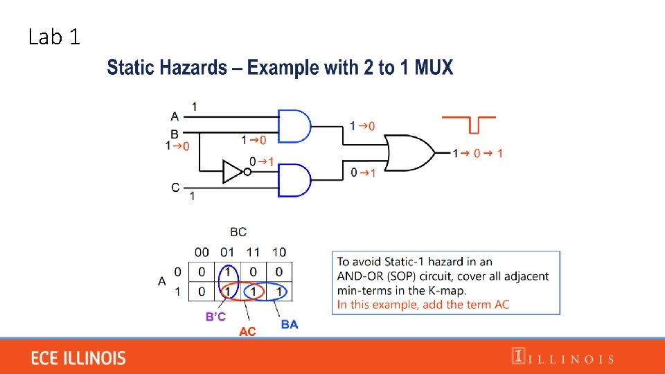
Lab 1

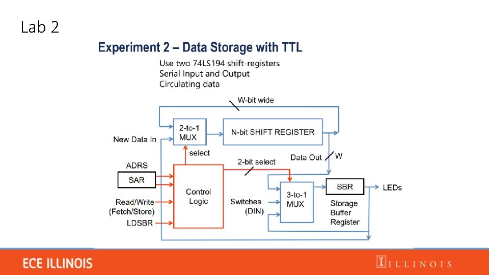
Lab 2

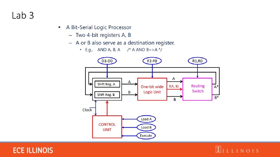
Lab 3

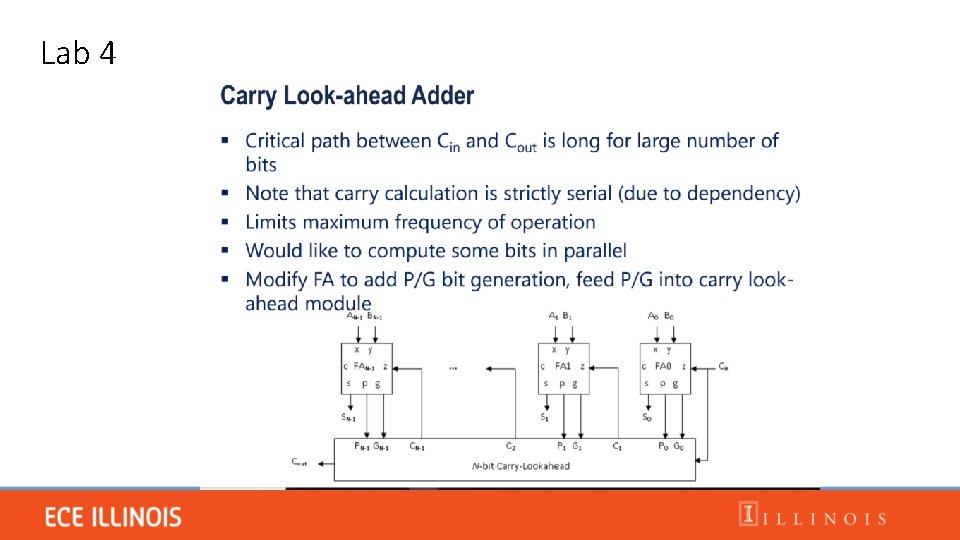
Lab 4

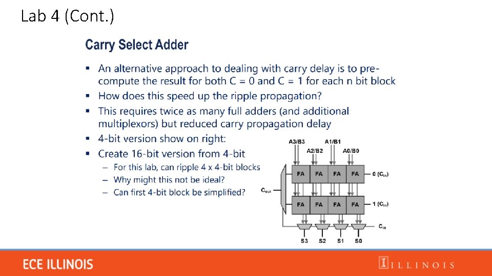
Lab 4 (Cont. )

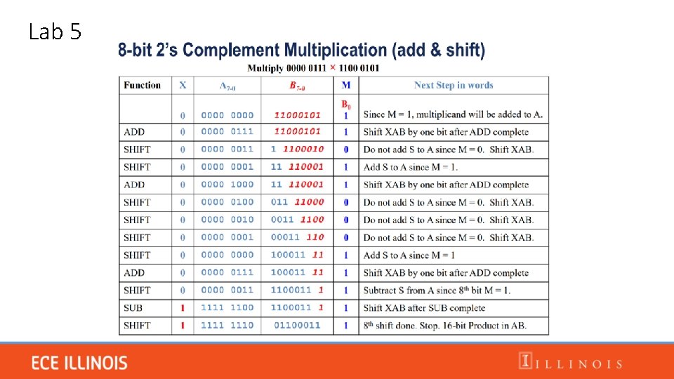
Lab 5

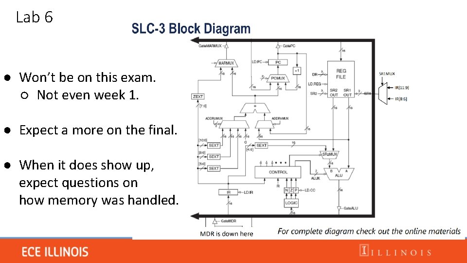
Lab 6 ● Won’t be on this exam. ○ Not even week 1. ● Expect a more on the final. ● When it does show up, expect questions on how memory was handled.

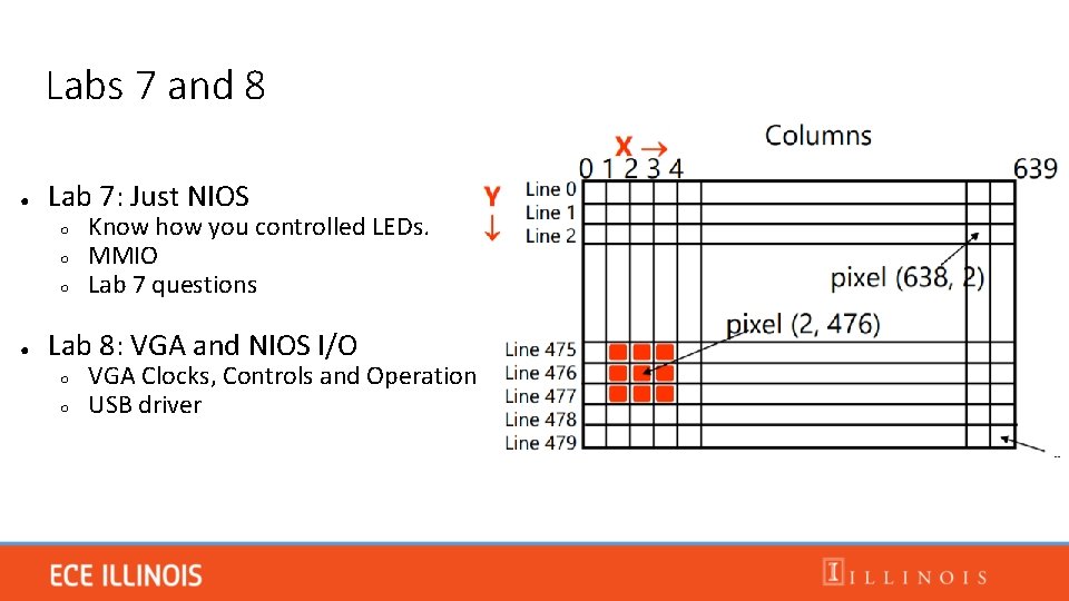
Labs 7 and 8 ● Lab 7: Just NIOS ○ ○ ○ ● Know how you controlled LEDs. MMIO Lab 7 questions Lab 8: VGA and NIOS I/O ○ ○ VGA Clocks, Controls and Operation USB driver

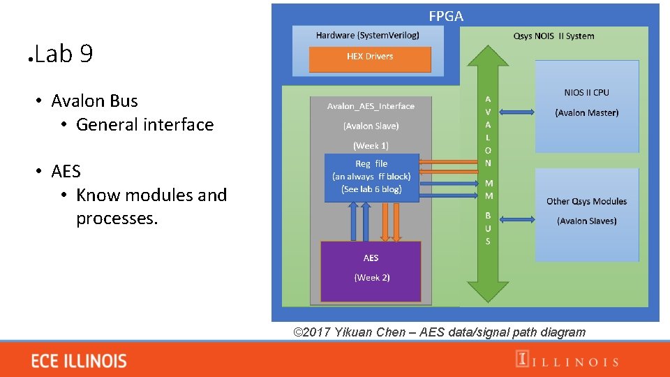
● Lab 9 • Avalon Bus • General interface • AES • Know modules and processes. © 2017 Yikuan Chen – AES data/signal path diagram

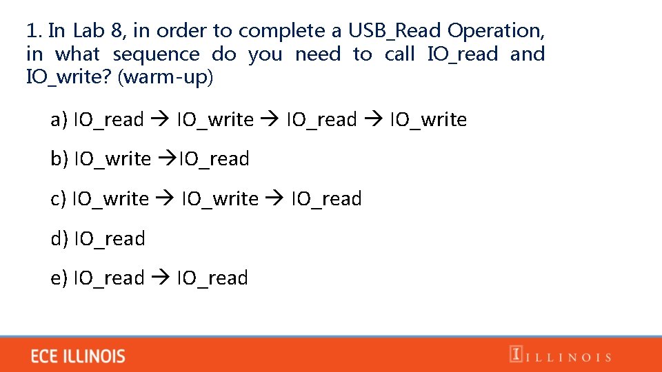
1. In Lab 8, in order to complete a USB_Read Operation, in what sequence do you need to call IO_read and IO_write? (warm-up) a) IO_read IO_write b) IO_write IO_read c) IO_write IO_read d) IO_read e) IO_read

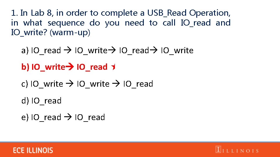
1. In Lab 8, in order to complete a USB_Read Operation, in what sequence do you need to call IO_read and IO_write? (warm-up) a) IO_read IO_write IO_read IO_write b) IO_write IO_read ★ c) IO_write IO_read d) IO_read e) IO_read

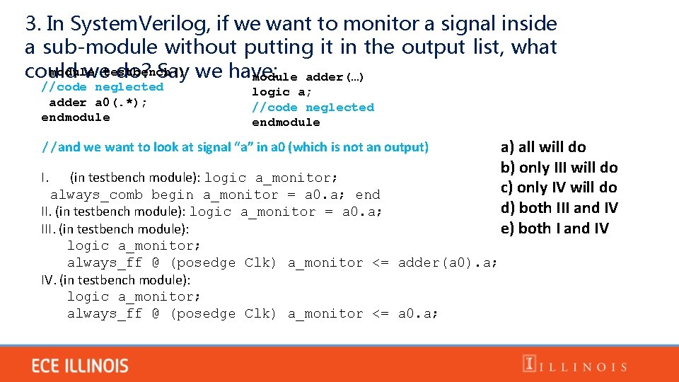
3. In System. Verilog, if we want to monitor a signal inside a sub-module without putting it in the output list, what module could wetestbench() do? Say we have: module adder(…) //code neglected adder a 0(. *); endmodule logic a; //code neglected endmodule //and we want to look at signal “a” in a 0 (which is not an output) I. (in testbench module): logic a_monitor; always_comb begin a_monitor = a 0. a; end II. (in testbench module): logic a_monitor = a 0. a; III. (in testbench module): logic a_monitor; always_ff @ (posedge Clk) a_monitor <= adder(a 0). a; IV. (in testbench module): logic a_monitor; always_ff @ (posedge Clk) a_monitor <= a 0. a; a) all will do b) only III will do c) only IV will do d) both III and IV e) both I and IV

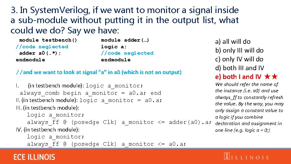
3. In System. Verilog, if we want to monitor a signal inside a sub-module without putting it in the output list, what could we do? Say we have: module testbench() //code neglected adder a 0(. *); endmodule adder(…) logic a; //code neglected endmodule //and we want to look at signal “a” in a 0 (which is not an output) a) all will do b) only III will do c) only IV will do d) both III and IV e) both I and IV ★★ We should refer the name of (in testbench module): logic a_monitor; the instance (i. e. a 0) and use always_comb begin a_monitor = a 0. a; end always_ff to constantly refresh II. (in testbench module): logic a_monitor = a 0. a; the value. By the way, you may III. (in testbench module): only assign a constant value to logic a_monitor; a logic if you combine always_ff @ (posedge Clk) a_monitor <= adder(a 0). a; declaration and assignment in IV. (in testbench module): one line (e. g. logic a = 0; ) logic a_monitor; always_ff @ (posedge Clk) a_monitor <= a 0. a; I.

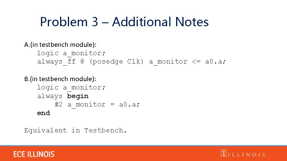
Problem 3 – Additional Notes A. (in testbench module): logic a_monitor; always_ff @ (posedge Clk) a_monitor <= a 0. a; B. (in testbench module): logic a_monitor; always begin #2 a_monitor = a 0. a; end Equivalent in Testbench.

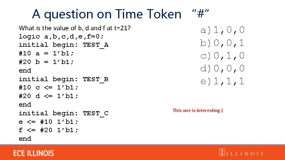
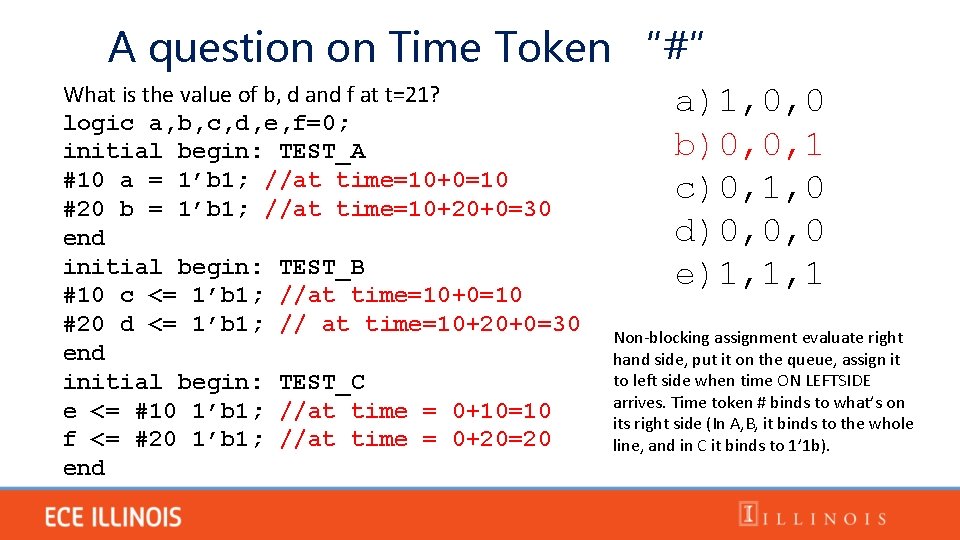
A question on Time Token “#” What is the value of b, d and f at t=21? logic a, b, c, d, e, f=0; initial begin: TEST_A #10 a = 1’b 1; #20 b = 1’b 1; end initial begin: TEST_B #10 c <= 1’b 1; #20 d <= 1’b 1; end initial begin: TEST_C e <= #10 1’b 1; f <= #20 1’b 1; end a)1, 0, 0 b)0, 0, 1 c)0, 1, 0 d)0, 0, 0 e)1, 1, 1 This one is interesting: )

A question on Time Token “#” What is the value of b, d and f at t=21? logic a, b, c, d, e, f=0; initial begin: TEST_A #10 a = 1’b 1; //at time=10+0=10 #20 b = 1’b 1; //at time=10+20+0=30 end initial begin: TEST_B #10 c <= 1’b 1; //at time=10+0=10 #20 d <= 1’b 1; // at time=10+20+0=30 end initial begin: TEST_C e <= #10 1’b 1; //at time = 0+10=10 f <= #20 1’b 1; //at time = 0+20=20 end a)1, 0, 0 b)0, 0, 1 c)0, 1, 0 d)0, 0, 0 e)1, 1, 1 Non-blocking assignment evaluate right hand side, put it on the queue, assign it to left side when time ON LEFTSIDE arrives. Time token # binds to what’s on its right side (In A, B, it binds to the whole line, and in C it binds to 1’ 1 b).

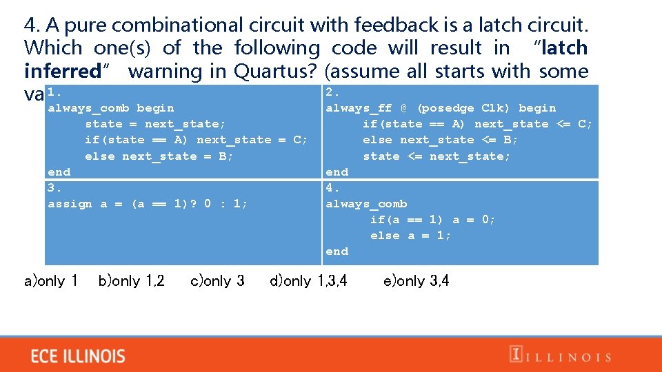
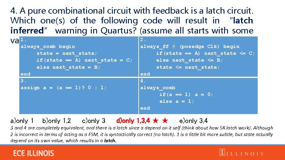
4. A pure combinational circuit with feedback is a latch circuit. Which one(s) of the following code will result in “latch inferred” warning in Quartus? (assume all starts with some 1. value) 2. valid always_comb begin state = next_state; if(state == A) next_state = C; else next_state = B; end 3. assign a = (a == 1)? 0 : 1; a)only 1 b)only 1, 2 c)only 3 always_ff @ (posedge Clk) begin if(state == A) next_state <= C; else next_state <= B; state <= next_state; end 4. always_comb if(a == 1) a = 0; else a = 1; end d)only 1, 3, 4 e)only 3, 4

4. A pure combinational circuit with feedback is a latch circuit. Which one(s) of the following code will result in “latch inferred” warning in Quartus? (assume all starts with some 1. value) 2. valid always_comb begin state = next_state; if(state == A) next_state = C; else next_state = B; end 3. assign a = (a == 1)? 0 : 1; a)only 1 b)only 1, 2 c)only 3 always_ff @ (posedge Clk) begin if(state == A) next_state <= C; else next_state <= B; state <= next_state; end 4. always_comb if(a == 1) a = 0; else a = 1; end d)only 1, 3, 4 ★ ★ e)only 3, 4 3 and 4 are completely equivalent, and there is a latch since a depend on it self (think about how SR latch work). Although 2 is incorrect in terms of acting as a FSM, it is syntactically correct (no latch). 1 is a little bit more subtle, but state actually depend on its own value, which results in a latch.

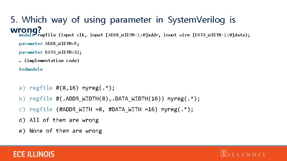
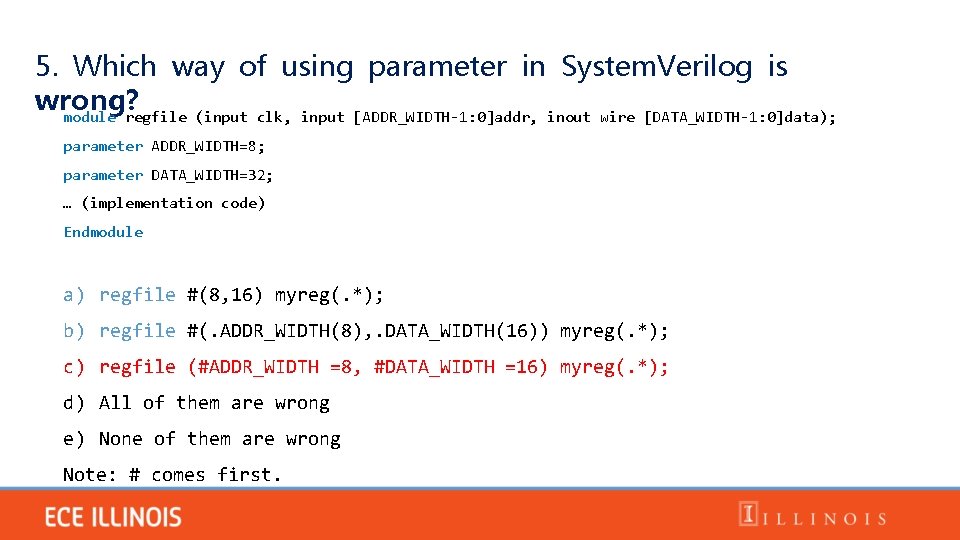
5. Which way of using parameter in System. Verilog is wrong? module regfile (input clk, input [ADDR_WIDTH-1: 0]addr, inout wire [DATA_WIDTH-1: 0]data); parameter ADDR_WIDTH=8; parameter DATA_WIDTH=32; … (implementation code) Endmodule a) regfile #(8, 16) myreg(. *); b) regfile #(. ADDR_WIDTH(8), . DATA_WIDTH(16)) myreg(. *); c) regfile (#ADDR_WITH =8, #DATA_WITH =16) myreg(. *); d) All of them are wrong e) None of them are wrong

5. Which way of using parameter in System. Verilog is wrong? module regfile (input clk, input [ADDR_WIDTH-1: 0]addr, inout wire [DATA_WIDTH-1: 0]data); parameter ADDR_WIDTH=8; parameter DATA_WIDTH=32; … (implementation code) Endmodule a) regfile #(8, 16) myreg(. *); b) regfile #(. ADDR_WIDTH(8), . DATA_WIDTH(16)) myreg(. *); c) regfile (#ADDR_WIDTH =8, #DATA_WIDTH =16) myreg(. *); d) All of them are wrong e) None of them are wrong Note: # comes first.

6. What type of architecture does NIOS IIe belong to? a) b) c) d) e) A Moore Machine A Mealy Machine A Von-Neumann Machine A Harvard Machine A Modified Harvard Machine

6. What type of architecture does NIOS IIe belong to? a) b) c) d) e) A Moore Machine A Mealy Machine A Von-Neumann Machine A Harvard Machine A Modified Harvard Machine ★ The original Harvard Machine uses entirely separate memory system to store instructions and data.

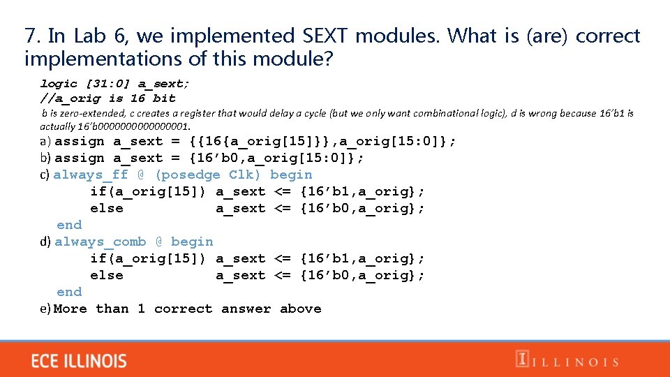
7. In Lab 6, we implemented SEXT modules. What is (are) correct implementations of this module? logic [31: 0] a_sext; //a_orig is 16 bit b is zero-extended, c creates a register that would delay a cycle (but we only want combinational logic), d is wrong because 16’b 1 is actually 16’b 000000001. a)assign a_sext = {{16{a_orig[15]}}, a_orig[15: 0]}; b) assign a_sext = {16’b 0, a_orig[15: 0]}; c) always_ff @ (posedge Clk) begin if(a_orig[15]) a_sext <= {16’b 1, a_orig}; else a_sext <= {16’b 0, a_orig}; end d) always_comb @ begin if(a_orig[15]) a_sext <= {16’b 1, a_orig}; else a_sext <= {16’b 0, a_orig}; end e) More than 1 correct answer above

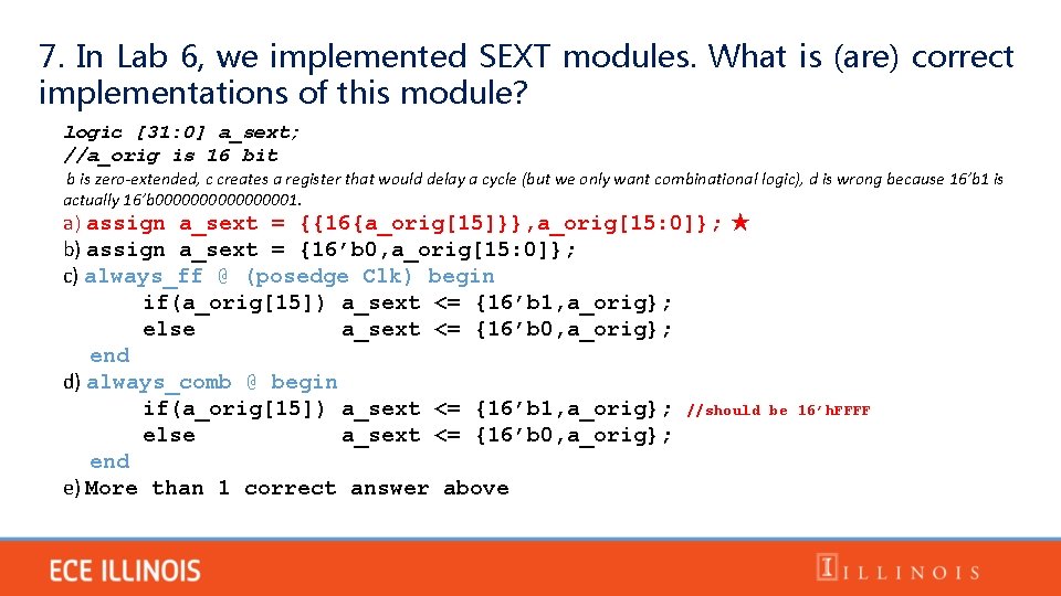
7. In Lab 6, we implemented SEXT modules. What is (are) correct implementations of this module? logic [31: 0] a_sext; //a_orig is 16 bit b is zero-extended, c creates a register that would delay a cycle (but we only want combinational logic), d is wrong because 16’b 1 is actually 16’b 000000001. a)assign a_sext = {{16{a_orig[15]}}, a_orig[15: 0]}; ★ b) assign a_sext = {16’b 0, a_orig[15: 0]}; c) always_ff @ (posedge Clk) begin if(a_orig[15]) a_sext <= {16’b 1, a_orig}; else a_sext <= {16’b 0, a_orig}; end d) always_comb @ begin if(a_orig[15]) a_sext <= {16’b 1, a_orig}; //should else a_sext <= {16’b 0, a_orig}; end e) More than 1 correct answer above be 16’h. FFFF

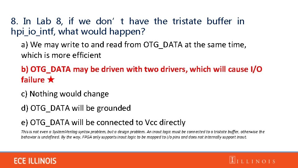
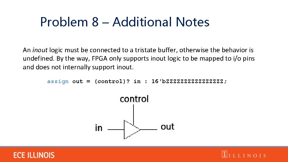
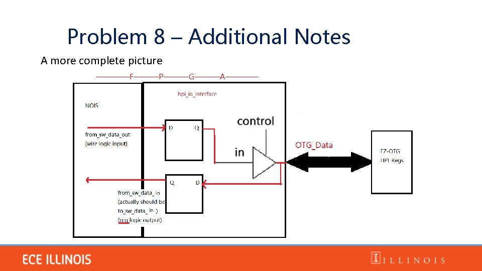
8. In Lab 8, if we don’t have the tristate buffer in hpi_io_intf, what would happen? a) We may write to and read from OTG_DATA at the same time, which is more efficient b) OTG_DATA may be driven with two drivers, which will cause I/O failure c) Nothing would change d) OTG_DATA will be grounded e) OTG_DATA will be connected to Vcc directly This is not even a System. Verilog syntax problem, but a design problem. An inout logic must be connected to a tristate buffer, otherwise the behavior is undefined. By the way, FPGA only supports inout logic to be mapped to i/o pins and does not internally support inout.

8. In Lab 8, if we don’t have the tristate buffer in hpi_io_intf, what would happen? a) We may write to and read from OTG_DATA at the same time, which is more efficient b) OTG_DATA may be driven with two drivers, which will cause I/O failure ★ c) Nothing would change d) OTG_DATA will be grounded e) OTG_DATA will be connected to Vcc directly This is not even a System. Verilog syntax problem, but a design problem. An inout logic must be connected to a tristate buffer, otherwise the behavior is undefined. By the way, FPGA only supports inout logic to be mapped to i/o pins and does not internally support inout.

Problem 8 – Additional Notes An inout logic must be connected to a tristate buffer, otherwise the behavior is undefined. By the way, FPGA only supports inout logic to be mapped to i/o pins and does not internally support inout. assign out = (control)? in : 16'b. ZZZZZZZZ;

Problem 8 – Additional Notes A more complete picture

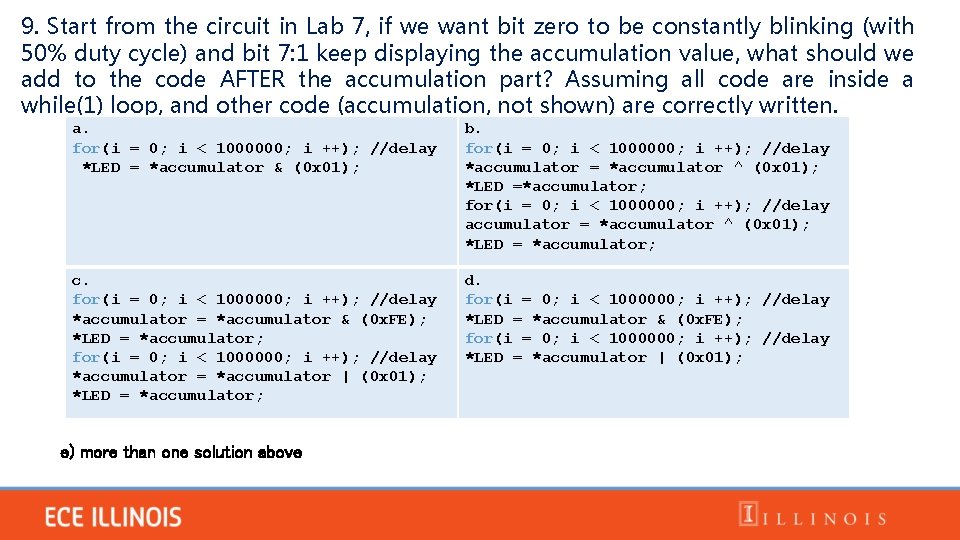
9. Start from the circuit in Lab 7, if we want bit zero to be constantly blinking (with 50% duty cycle) and bit 7: 1 keep displaying the accumulation value, what should we add to the code AFTER the accumulation part? Assuming all code are inside a while(1) loop, and other code (accumulation, not shown) are correctly written. a. for(i = 0; i < 1000000; i ++); //delay *LED = *accumulator & (0 x 01); b. for(i = 0; i < 1000000; i ++); //delay *accumulator = *accumulator ^ (0 x 01); *LED =*accumulator; for(i = 0; i < 1000000; i ++); //delay accumulator = *accumulator ^ (0 x 01); *LED = *accumulator; c. for(i = 0; i < 1000000; i ++); //delay *accumulator = *accumulator & (0 x. FE); *LED = *accumulator; for(i = 0; i < 1000000; i ++); //delay *accumulator = *accumulator | (0 x 01); *LED = *accumulator; d. for(i = 0; i < 1000000; i ++); //delay *LED = *accumulator & (0 x. FE); for(i = 0; i < 1000000; i ++); //delay *LED = *accumulator | (0 x 01); e) more than one solution above

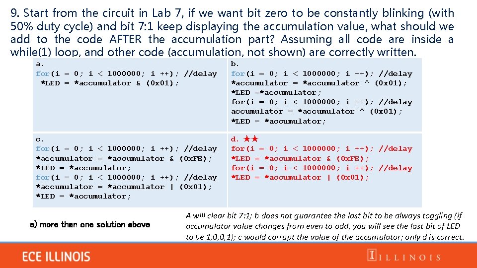
9. Start from the circuit in Lab 7, if we want bit zero to be constantly blinking (with 50% duty cycle) and bit 7: 1 keep displaying the accumulation value, what should we add to the code AFTER the accumulation part? Assuming all code are inside a while(1) loop, and other code (accumulation, not shown) are correctly written. a. for(i = 0; i < 1000000; i ++); //delay *LED = *accumulator & (0 x 01); b. for(i = 0; i < 1000000; i ++); //delay *accumulator = *accumulator ^ (0 x 01); *LED =*accumulator; for(i = 0; i < 1000000; i ++); //delay accumulator = *accumulator ^ (0 x 01); *LED = *accumulator; c. for(i = 0; i < 1000000; i ++); //delay *accumulator = *accumulator & (0 x. FE); *LED = *accumulator; for(i = 0; i < 1000000; i ++); //delay *accumulator = *accumulator | (0 x 01); *LED = *accumulator; d. ★★ for(i = 0; i < 1000000; i ++); //delay *LED = *accumulator & (0 x. FE); for(i = 0; i < 1000000; i ++); //delay *LED = *accumulator | (0 x 01); e) more than one solution above A will clear bit 7: 1; b does not guarantee the last bit to be always toggling (if accumulator value changes from even to odd, you will see the last bit of LED to be 1, 0, 0, 1); c would corrupt the value of the accumulator; only d is correct.

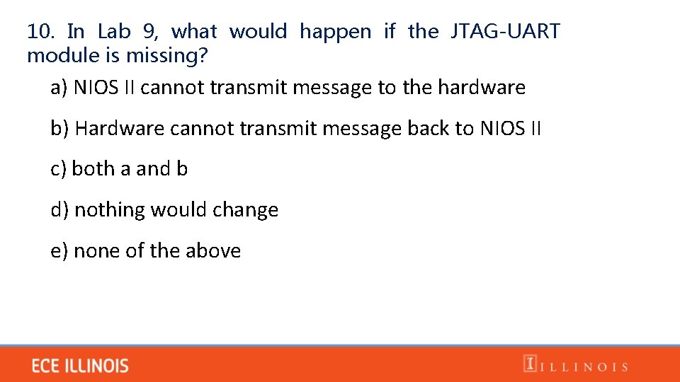
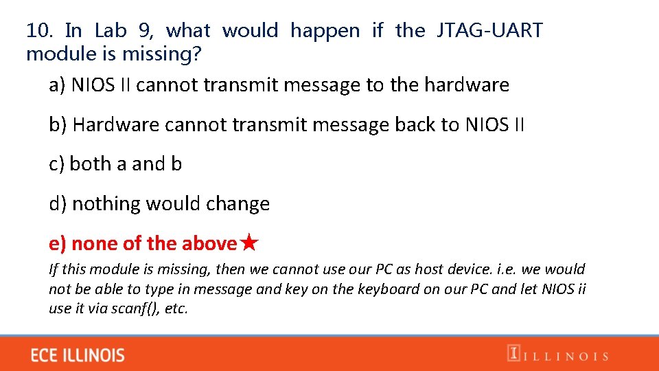
10. In Lab 9, what would happen if the JTAG-UART module is missing? a) NIOS II cannot transmit message to the hardware b) Hardware cannot transmit message back to NIOS II c) both a and b d) nothing would change e) none of the above

10. In Lab 9, what would happen if the JTAG-UART module is missing? a) NIOS II cannot transmit message to the hardware b) Hardware cannot transmit message back to NIOS II c) both a and b d) nothing would change e) none of the above★ If this module is missing, then we cannot use our PC as host device. i. e. we would not be able to type in message and key on the keyboard on our PC and let NIOS ii use it via scanf(), etc.

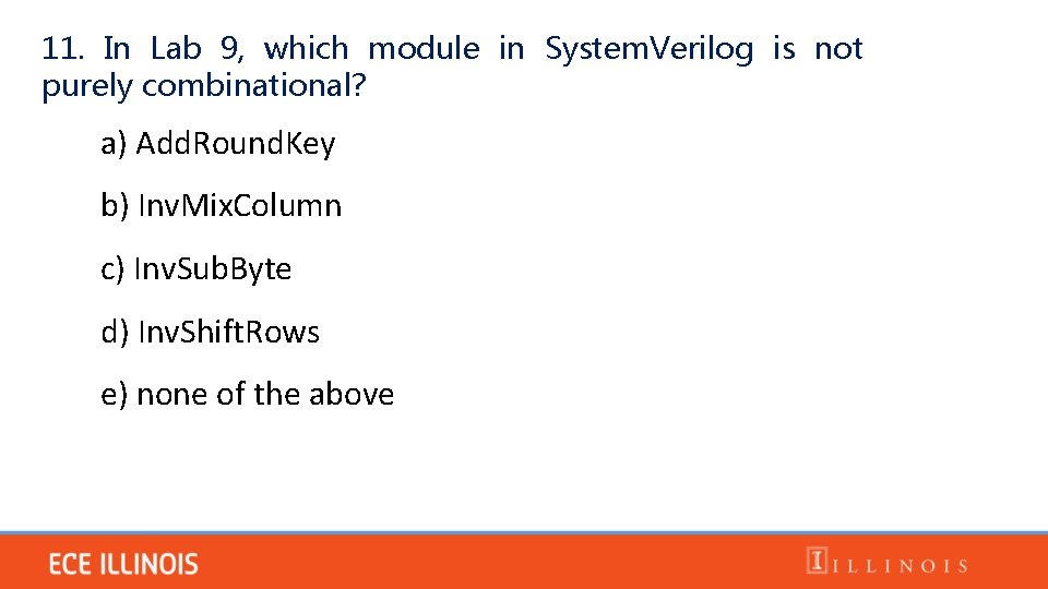
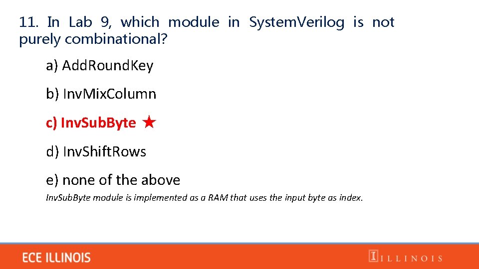
11. In Lab 9, which module in System. Verilog is not purely combinational? a) Add. Round. Key b) Inv. Mix. Column c) Inv. Sub. Byte d) Inv. Shift. Rows e) none of the above

11. In Lab 9, which module in System. Verilog is not purely combinational? a) Add. Round. Key b) Inv. Mix. Column c) Inv. Sub. Byte ★ d) Inv. Shift. Rows e) none of the above Inv. Sub. Byte module is implemented as a RAM that uses the input byte as index.

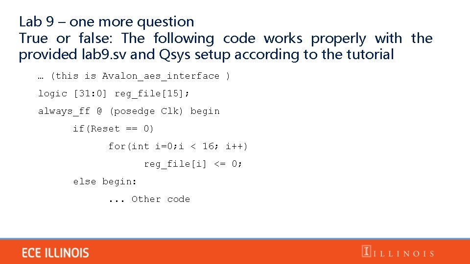
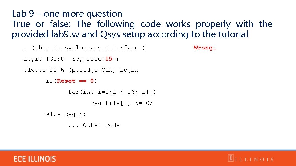
Lab 9 – one more question True or false: The following code works properly with the provided lab 9. sv and Qsys setup according to the tutorial … (this is Avalon_aes_interface ) logic [31: 0] reg_file[15]; always_ff @ (posedge Clk) begin if(Reset == 0) for(int i=0; i < 16; i++) reg_file[i] <= 0; else begin: . . . Other code

Lab 9 – one more question True or false: The following code works properly with the provided lab 9. sv and Qsys setup according to the tutorial … (this is Avalon_aes_interface ) logic [31: 0] reg_file[15]; always_ff @ (posedge Clk) begin if(Reset == 0) for(int i=0; i < 16; i++) reg_file[i] <= 0; else begin: . . . Other code Wrong…

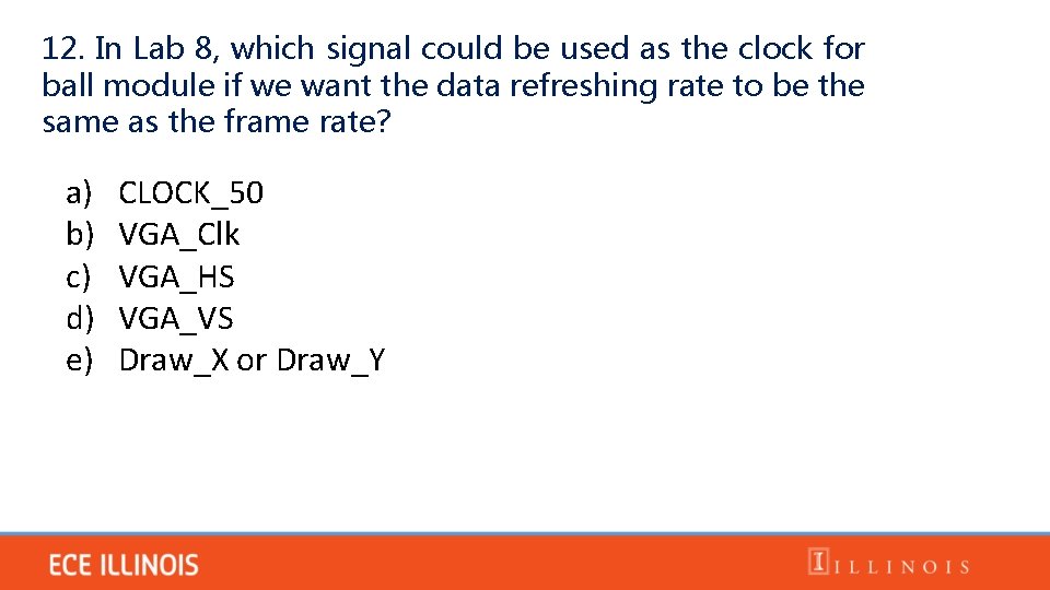
12. In Lab 8, which signal could be used as the clock for ball module if we want the data refreshing rate to be the same as the frame rate? a) b) c) d) e) CLOCK_50 VGA_Clk VGA_HS VGA_VS Draw_X or Draw_Y

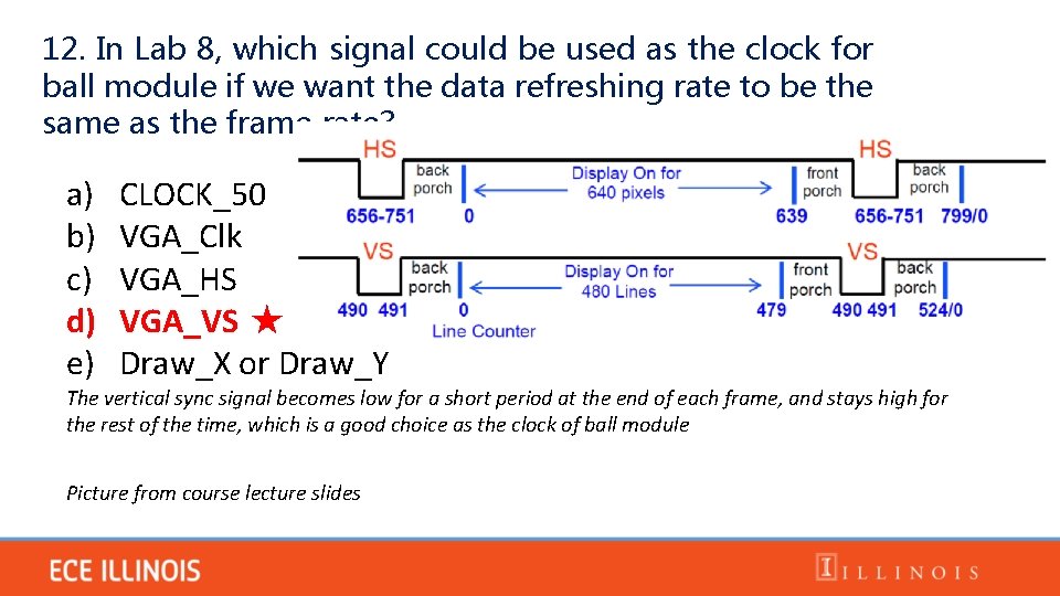
12. In Lab 8, which signal could be used as the clock for ball module if we want the data refreshing rate to be the same as the frame rate? a) b) c) d) e) CLOCK_50 VGA_Clk VGA_HS VGA_VS ★ Draw_X or Draw_Y The vertical sync signal becomes low for a short period at the end of each frame, and stays high for the rest of the time, which is a good choice as the clock of ball module Picture from course lecture slides

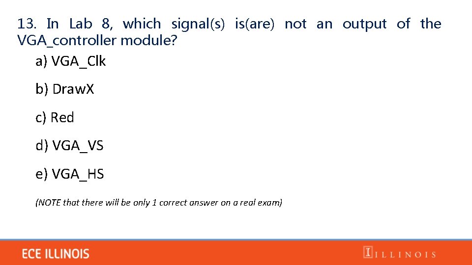
13. In Lab 8, which signal(s) is(are) not an output of the VGA_controller module? a) VGA_Clk b) Draw. X c) Red d) VGA_VS e) VGA_HS (NOTE that there will be only 1 correct answer on a real exam)

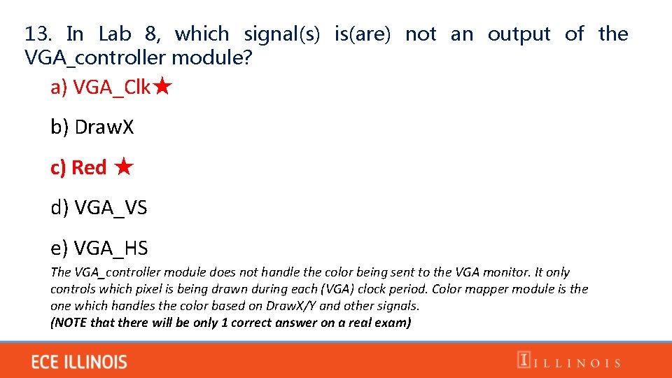
13. In Lab 8, which signal(s) is(are) not an output of the VGA_controller module? a) VGA_Clk★ b) Draw. X c) Red ★ d) VGA_VS e) VGA_HS The VGA_controller module does not handle the color being sent to the VGA monitor. It only controls which pixel is being drawn during each (VGA) clock period. Color mapper module is the one which handles the color based on Draw. X/Y and other signals. (NOTE that there will be only 1 correct answer on a real exam)

14. True or False: SDRAM is faster than SRAM (since SDRAM is Dynamic RAM) a) True b) False

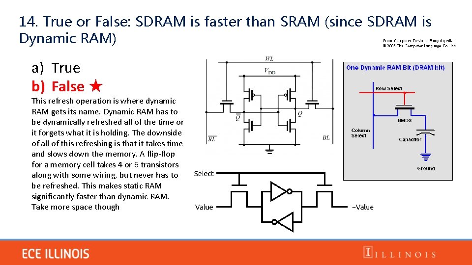
14. True or False: SDRAM is faster than SRAM (since SDRAM is Dynamic RAM) a) True b) False ★ This refresh operation is where dynamic RAM gets its name. Dynamic RAM has to be dynamically refreshed all of the time or it forgets what it is holding. The downside of all of this refreshing is that it takes time and slows down the memory. A flip-flop for a memory cell takes 4 or 6 transistors along with some wiring, but never has to be refreshed. This makes static RAM significantly faster than dynamic RAM. Take more space though

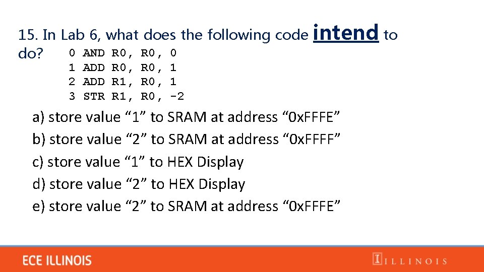
15. In Lab 6, what does the following code 0 AND R 0, 0 do? intend to 1 ADD R 0, 1 2 ADD R 1, R 0, 1 3 STR R 1, R 0, -2 a) store value “ 1” to SRAM at address “ 0 x. FFFE” b) store value “ 2” to SRAM at address “ 0 x. FFFF” c) store value “ 1” to HEX Display d) store value “ 2” to HEX Display e) store value “ 2” to SRAM at address “ 0 x. FFFE”

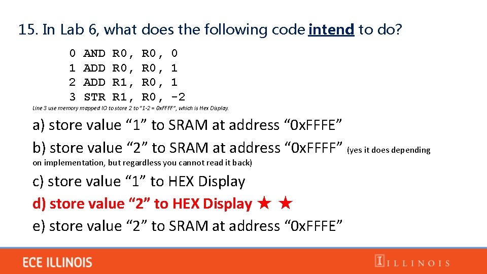
15. In Lab 6, what does the following code intend to do? 0 1 2 3 AND ADD STR R 0, R 1, R 0, 0 1 1 -2 Line 3 use memory mapped IO to store 2 to “ 1 -2 = 0 x. FFFF”, which is Hex Display. a) store value “ 1” to SRAM at address “ 0 x. FFFE” b) store value “ 2” to SRAM at address “ 0 x. FFFF” (yes it does depending on implementation, but regardless you cannot read it back) c) store value “ 1” to HEX Display d) store value “ 2” to HEX Display ★ ★ e) store value “ 2” to SRAM at address “ 0 x. FFFE”

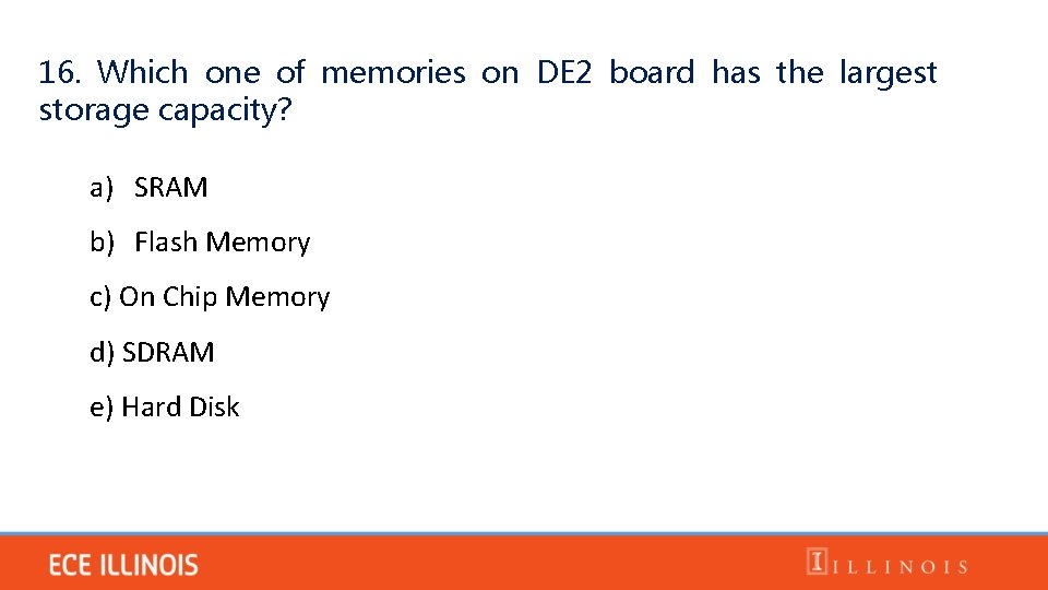
16. Which one of memories on DE 2 board has the largest storage capacity? a) SRAM b) Flash Memory c) On Chip Memory d) SDRAM e) Hard Disk

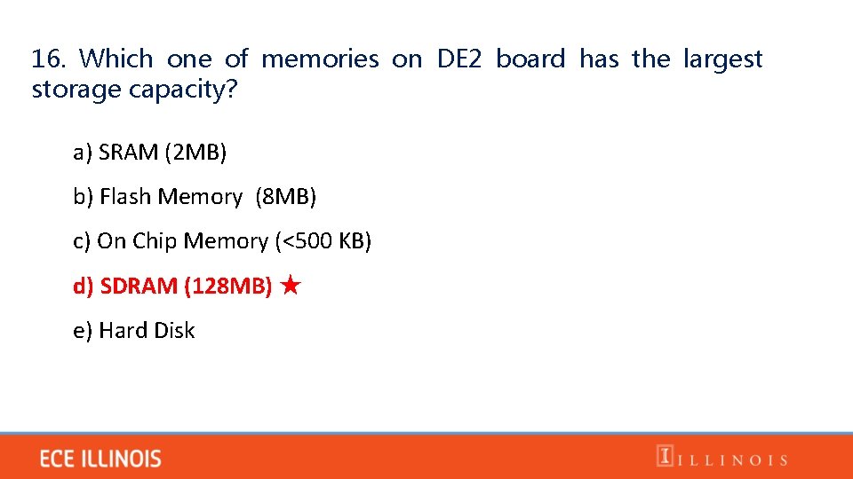
16. Which one of memories on DE 2 board has the largest storage capacity? a) SRAM (2 MB) b) Flash Memory (8 MB) c) On Chip Memory (<500 KB) d) SDRAM (128 MB) ★ e) Hard Disk

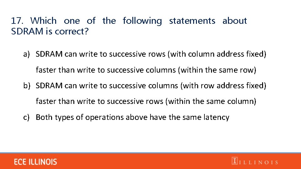
17. Which one of the following statements about SDRAM is correct? a) SDRAM can write to successive rows (with column address fixed) faster than write to successive columns (within the same row) b) SDRAM can write to successive columns (with row address fixed) faster than write to successive rows (within the same column) c) Both types of operations above have the same latency

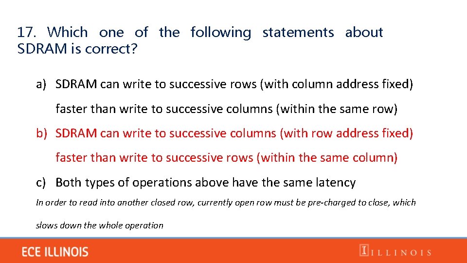
17. Which one of the following statements about SDRAM is correct? a) SDRAM can write to successive rows (with column address fixed) faster than write to successive columns (within the same row) b) SDRAM can write to successive columns (with row address fixed) faster than write to successive rows (within the same column) c) Both types of operations above have the same latency In order to read into another closed row, currently open row must be pre-charged to close, which slows down the whole operation

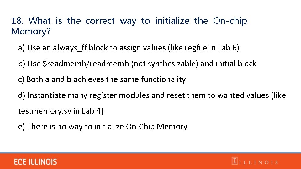
18. What is the correct way to initialize the On-chip Memory? a) Use an always_ff block to assign values (like regfile in Lab 6) b) Use $readmemh/readmemb (not synthesizable) and initial block c) Both a and b achieves the same functionality d) Instantiate many register modules and reset them to wanted values (like testmemory. sv in Lab 4) e) There is no way to initialize On-Chip Memory

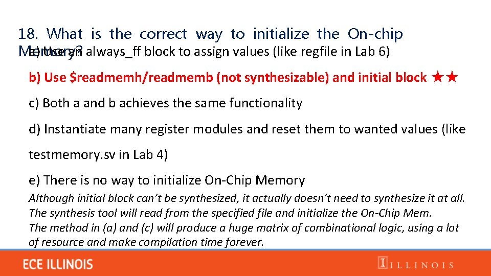
18. What is the correct way to initialize the On-chip a) Use an always_ff block to assign values (like regfile in Lab 6) Memory? b) Use $readmemh/readmemb (not synthesizable) and initial block ★★ c) Both a and b achieves the same functionality d) Instantiate many register modules and reset them to wanted values (like testmemory. sv in Lab 4) e) There is no way to initialize On-Chip Memory Although initial block can’t be synthesized, it actually doesn’t need to synthesize it at all. The synthesis tool will read from the specified file and initialize the On-Chip Mem. The method in (a) and (c) will produce a huge matrix of combinational logic, using a lot of resource and make compilation time forever.

• Again… • ~70% will be materials after Midterm; • ~30% will be materials before Midterm; • Know the high-level description (with a reasonable level of detail, of course) of each Lab is the most important thing. • Know the things discussed in lecture about Final Project will be helpful. • Know the properties of all the storages on the board (on chip memory, SRAM, SDRAM, Flash)

Study Resource 1. Course Wiki: Lecture Slides, Q/A session recording 2. Go to Monday Lecture and Ask Questions 3. Spend the same time on Final Exam would probably earn you more points than Final Project

Study Resources KTTECH ECE 385 Labs & Other Resources Midterm Practice Problems would be helpful for pre-midterm material