ECE 353 Introduction to Microprocessor Systems Week 10
- Slides: 43

ECE 353 Introduction to Microprocessor Systems Week 10 Michael J. Schulte

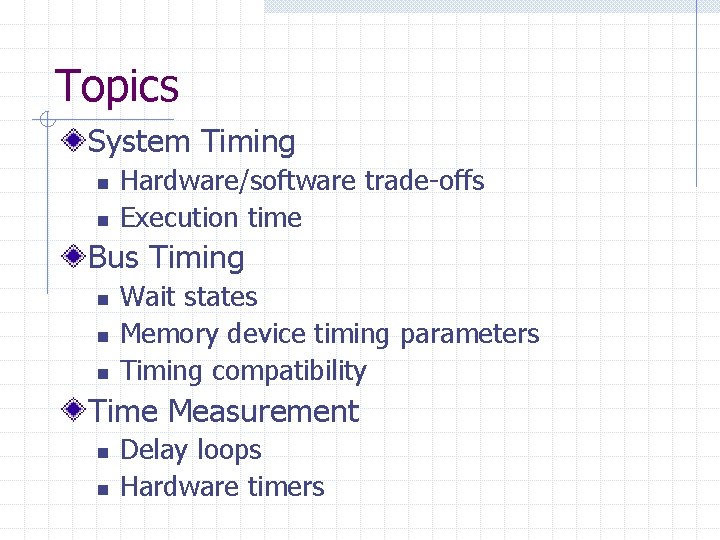
Topics System Timing n n Hardware/software trade-offs Execution time Bus Timing n n n Wait states Memory device timing parameters Timing compatibility Time Measurement n n Delay loops Hardware timers

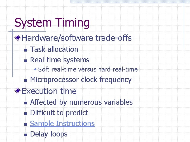
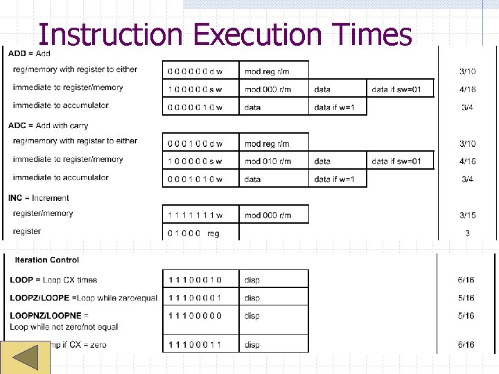
System Timing Hardware/software trade-offs n n Task allocation Real-time systems w Soft real-time versus hard real-time n Microprocessor clock frequency Execution time n n Affected by numerous variables Difficult to predict Sample Instructions Delay loops

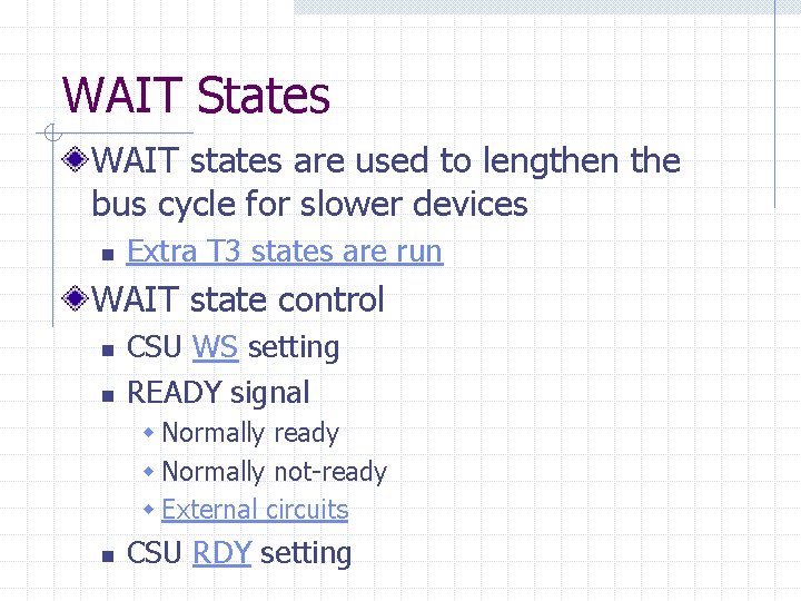
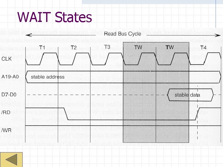
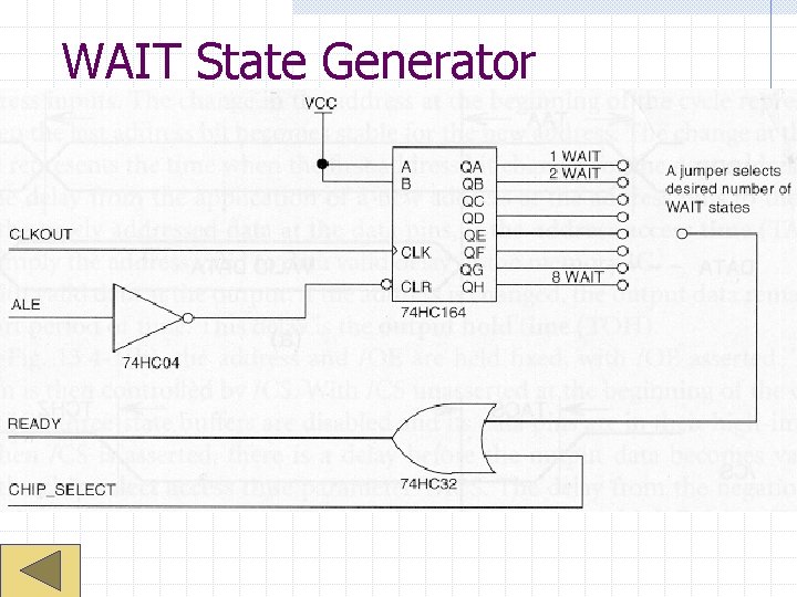
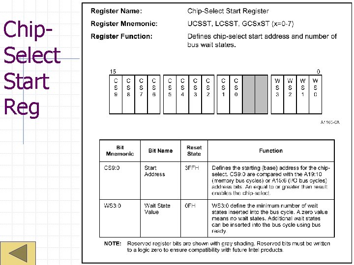
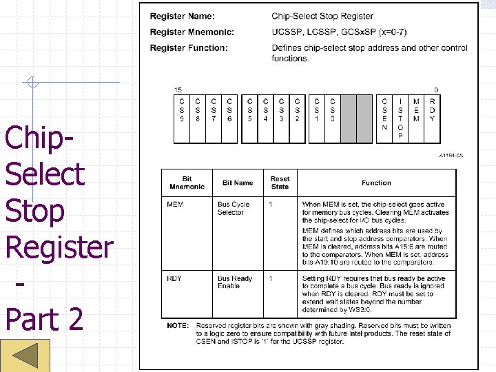
WAIT States WAIT states are used to lengthen the bus cycle for slower devices n Extra T 3 states are run WAIT state control n n CSU WS setting READY signal w Normally ready w Normally not-ready w External circuits n CSU RDY setting

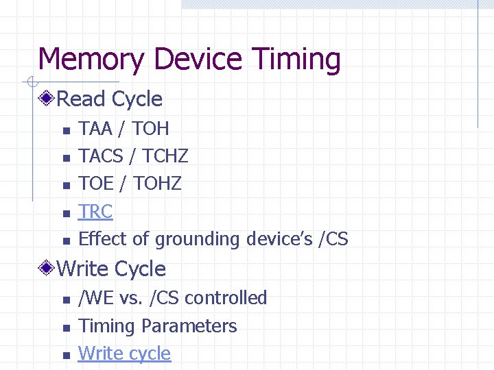
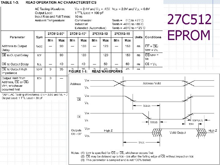
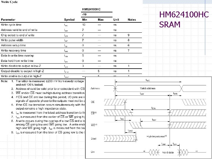
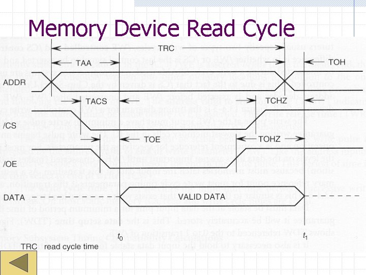
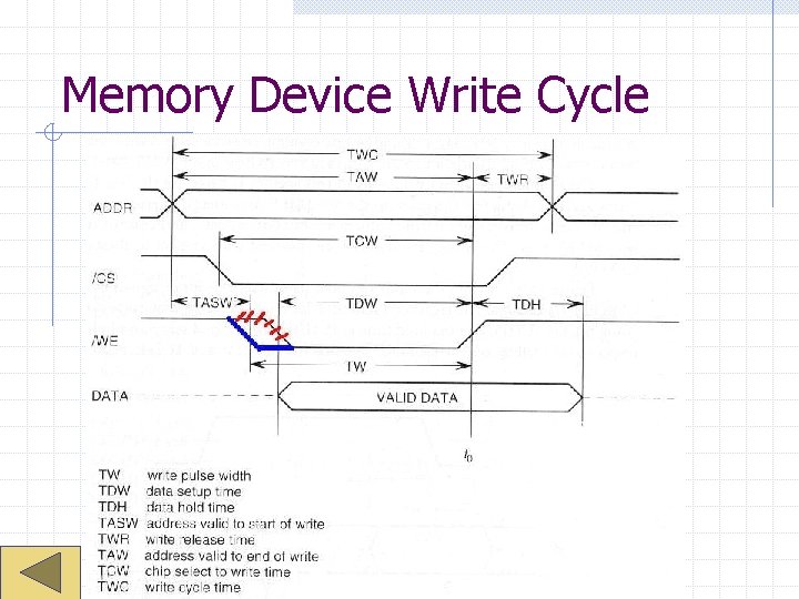
Memory Device Timing Read Cycle n n n TAA / TOH TACS / TCHZ TOE / TOHZ TRC Effect of grounding device’s /CS Write Cycle n n n /WE vs. /CS controlled Timing Parameters Write cycle

27 C 512 EPROM

HM 624100 HC SRAM

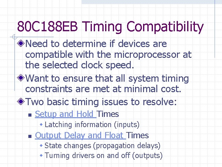
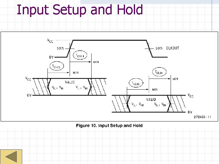
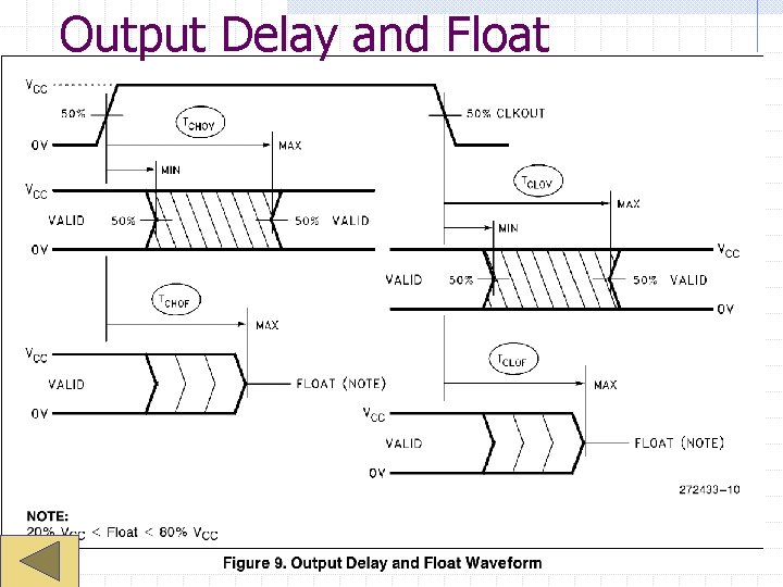
80 C 188 EB Timing Compatibility Need to determine if devices are compatible with the microprocessor at the selected clock speed. Want to ensure that all system timing constraints are met at minimal cost. Two basic timing issues to resolve: n Setup and Hold Times w Latching information (inputs) n Output Delay and Float Times w State changes (propagation delays) w Turning drivers on and off (outputs)

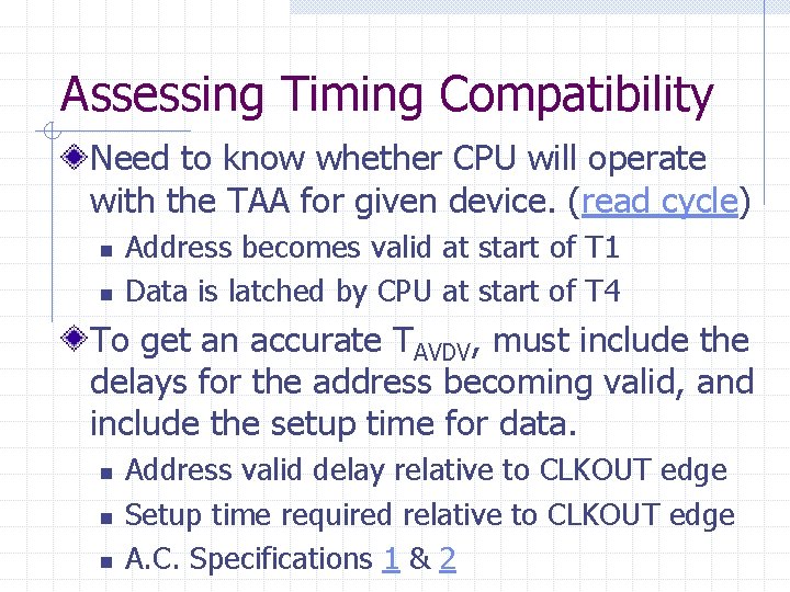
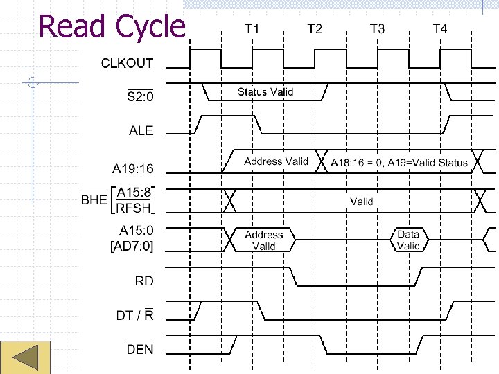
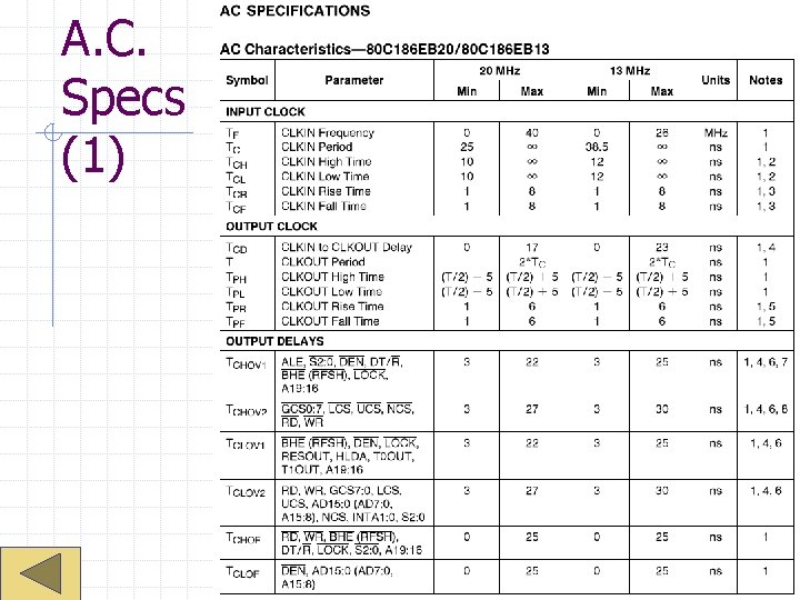
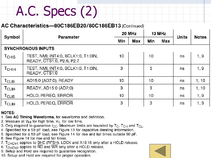
Assessing Timing Compatibility Need to know whether CPU will operate with the TAA for given device. (read cycle) n n Address becomes valid at start of T 1 Data is latched by CPU at start of T 4 To get an accurate TAVDV, must include the delays for the address becoming valid, and include the setup time for data. n n n Address valid delay relative to CLKOUT edge Setup time required relative to CLKOUT edge A. C. Specifications 1 & 2

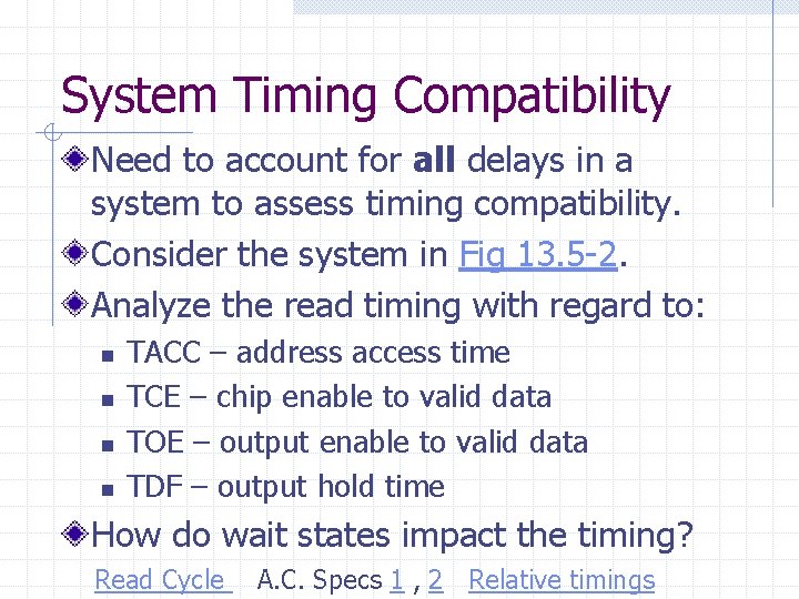
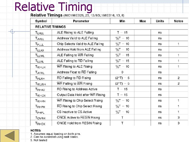
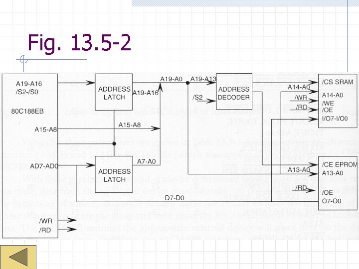
System Timing Compatibility Need to account for all delays in a system to assess timing compatibility. Consider the system in Fig 13. 5 -2. Analyze the read timing with regard to: n n TACC – address access time TCE – chip enable to valid data TOE – output enable to valid data TDF – output hold time How do wait states impact the timing? Read Cycle A. C. Specs 1 , 2 Relative timings

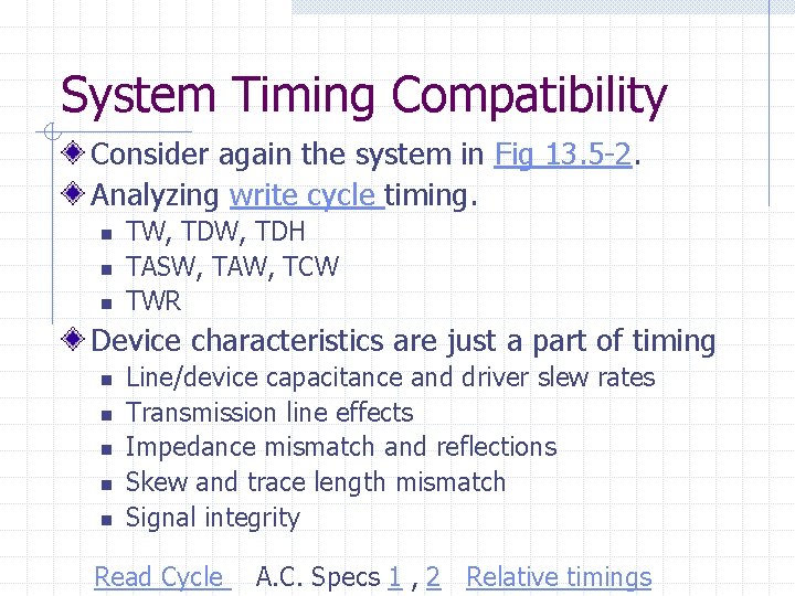
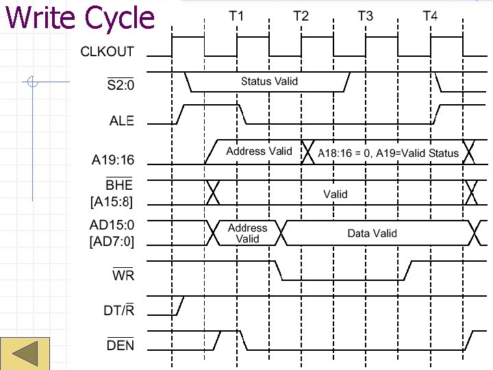
System Timing Compatibility Consider again the system in Fig 13. 5 -2. Analyzing write cycle timing. n n n TW, TDH TASW, TAW, TCW TWR Device characteristics are just a part of timing n n n Line/device capacitance and driver slew rates Transmission line effects Impedance mismatch and reflections Skew and trace length mismatch Signal integrity Read Cycle A. C. Specs 1 , 2 Relative timings

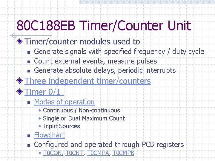
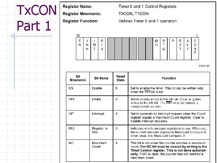
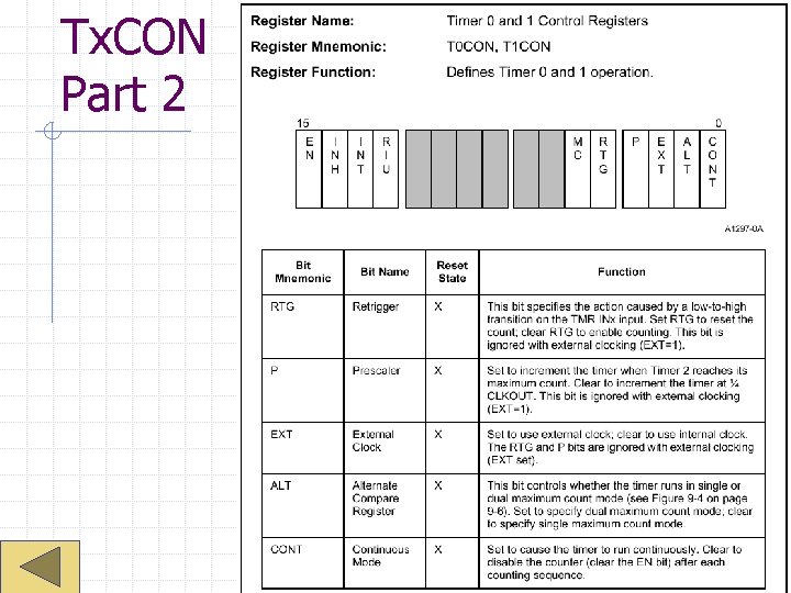
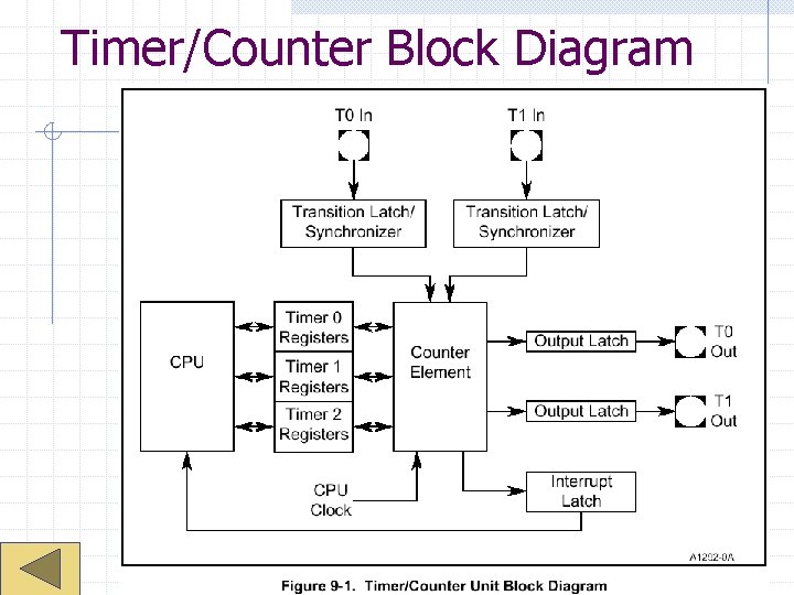
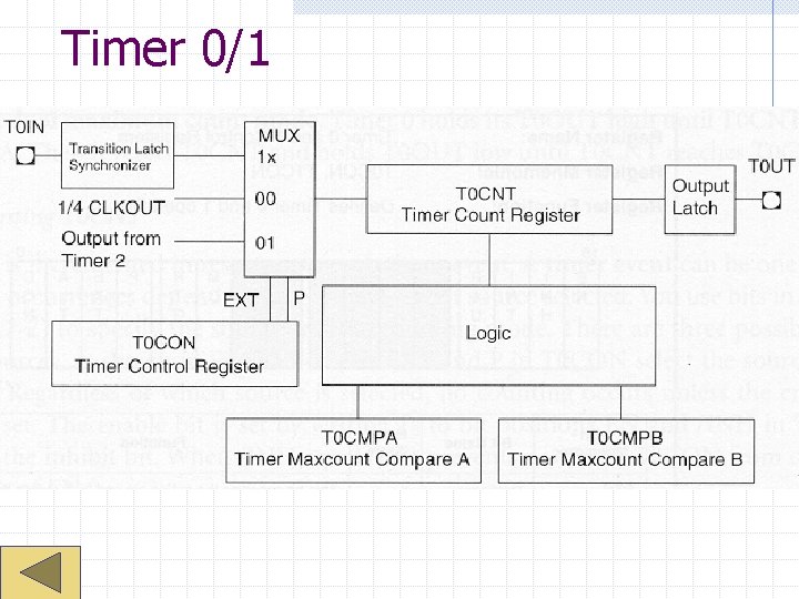
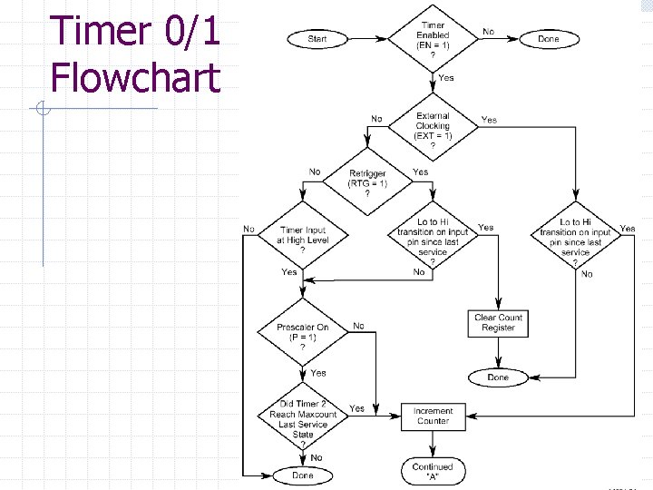
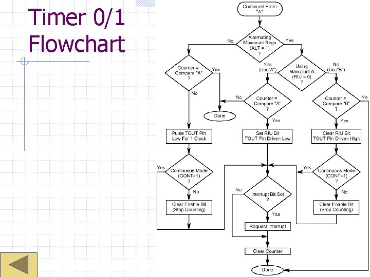
80 C 188 EB Timer/Counter Unit Timer/counter modules used to n n n Generate signals with specified frequency / duty cycle Count external events, measure pulses Generate absolute delays, periodic interrupts Three independent timer/counters Timer 0/1 n Modes of operation w Continuous / Non-continuous w Single or Dual Maximum Count w Input Sources n n Flowchart Configured and operated through PCB registers w T 0 CON, T 0 CNT, T 0 CMPA, T 0 CMPB

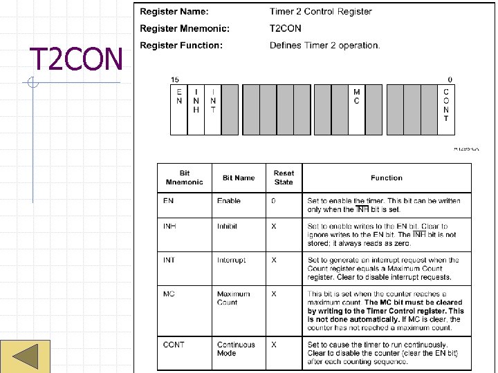
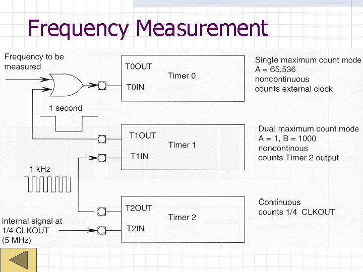
80 C 188 EB Timer/Counter Unit Timers 2 is much more limited. n Operated through PCB registers w T 2 CON, T 2 CNT, T 2 CMPA n Useful as a prescaler or as a periodic interrupt source. Timer applications n n Frequency measurement. Waveform generation.

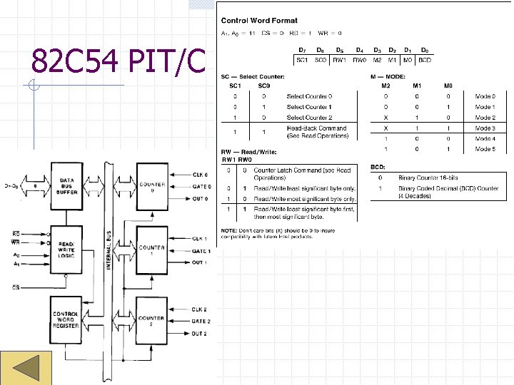
82 C 54 PIT/C Provides additional timer/counter resources for microprocessor system. n Appears as 4 byte-wide registers w Control register (3) w Timer registers (0, 1, 2) n Program by writing 3 bytes in sequence w Control byte w Timer word Three independent 16 -bit counters n n n BCD or binary DC-10 MHz input range Multiple modes of operation

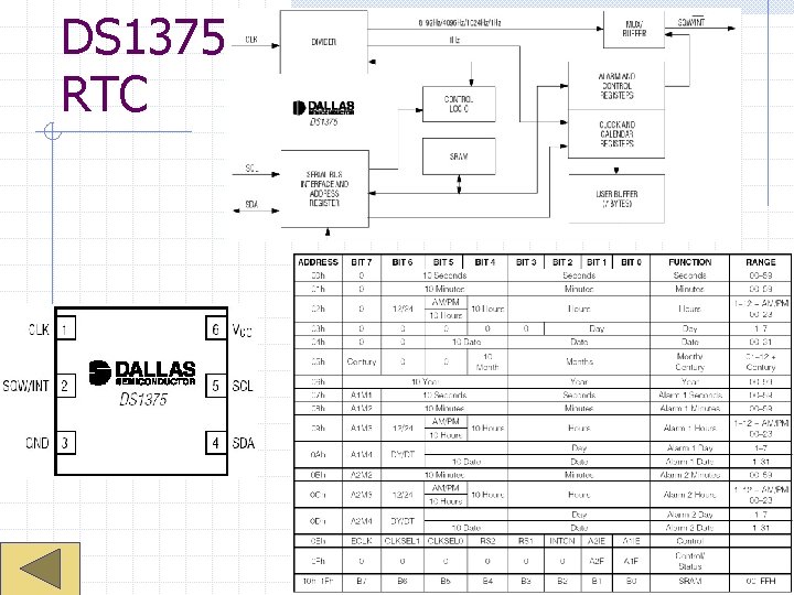
Real-Time Clocks (RTCs) RTCs provide microprocessor systems with absolute time information n n Absolute time does not necessarily mean calendar/clock time Typically operate from 32. 768 KHz crystal with battery or capacitor back-up power supply Generate periodic interrupts Often contain small amount of RAM – historically this was where the PC stored its configuration (BIOS) settings since it is nonvolatile. Dallas Semiconductor DS 1375

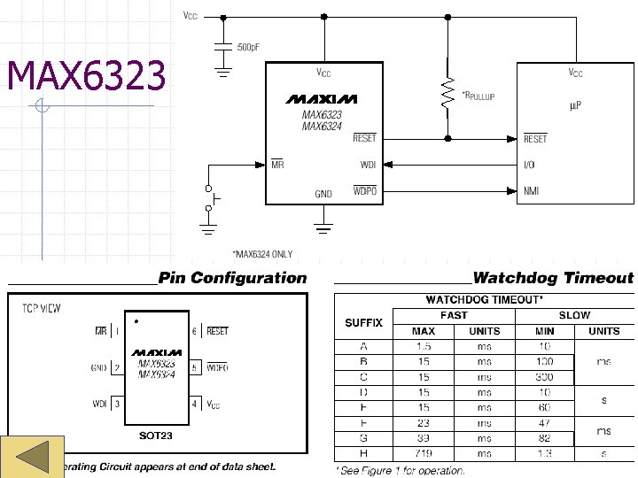
Watchdog Timers Watchdog timers are used to guard a system against lock-up due to software errors or soft failures in hardware. n Often included in CPU supervisor circuits. Retriggering usually done in the main program loop. Watchdog output can be used to reset the CPU or as a nonmaskable interrupt (NMI). Maxim MAX 6323/MAX 6324

WAIT States

WAIT State Generator

Chip. Select Start Reg

Chip. Select Stop Register Part 2

Memory Device Read Cycle

Memory Device Write Cycle

Instruction Execution Times

Input Setup and Hold

Output Delay and Float

Read Cycle

A. C. Specs (1)

A. C. Specs (2)

Relative Timing

Write Cycle

Fig. 13. 5 -2

Tx. CON Part 1

Tx. CON Part 2

T 2 CON

Timer/Counter Block Diagram

Timer 0/1

Timer Modes

Timer 0/1 Flowchart

Timer 0/1 Flowchart

Frequency Measurement

DS 1375 RTC

MAX 6323

82 C 54 PIT/C