ECE 3130 Digital Electronics and Design Lab 7

ECE 3130 – Digital Electronics and Design Lab 7 Shift Register Fall 2016

Introduction �A shift register is a cascade of flipflops that allows the bit-wise movement of the data contained within it. �Today we will… ◦ Design a bidirectional(shift right & shift left), parallel-load shift register using DFFs. ◦ Implement a clear control to reset the register to 0.

Shift-register SIPO - Serial In, Parallel Out PIPO – Parallel In, Parallel Out

Schematic Design Buffer DFF with clear pin

BUFFER

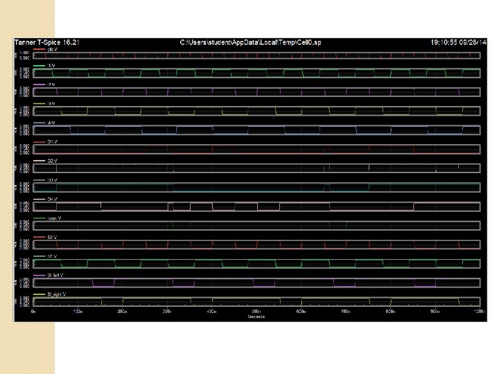
Function table for the register Mode control Register Operation S 1 S 0 0 0 No change 0 1 Shift Right 1 0 Shift Left 1 1 Parallel Load

In Mode#1: Input S 0=0, S 1=0. Other input pins are not used. The outputs O 1 -O 4 will not change in this mode. In Mode#2 (SIPO): Input S 0=1, S 1=0. “shift_right” pin is used to provide serial 1 -bit input data. Other input pins are not used. In Mode#3 (SIPO): Input S 0=0, S 1=1. “shift_left” pin is used to provide serial 1 -bit input data. Other input pins are not used. In Mode#4 (PIPO): Input S 0=1, S 1=1. I 1, I 2, I 3, I 4 are used to provide parallel 4 -bit input data. Other input pins are not used. The outputs O 1 -O 4 will be loaded to same value as inputs I 1 -I 4. For all modes(Mode#1 -4): Input “clk” pin is used to provide clock signal to DFFs. Input “clear” pin is used to reset all DFFs’ outputs to 0.

Shift Register

Symbol of Shift Register

Assignment �Build and test a Shift Register that has 4 different modes. �Attach all screenshots into one PDF file, including schematic, symbol, test circuit schematic, waveforms.
- Slides: 11