
ECE 2560 Binary number system Department of Electrical
ECE 2560 Binary number system Department of Electrical and Computer Engineering The Ohio State University ECE 3561 - Lecture 1 1
Today l Number systems l To and from base 10 l Addition l Subtraction (made easy) l Multiplication l THIS LECTURE IS REVIEW MATERIAL ECE 3561 - Lecture 1 2
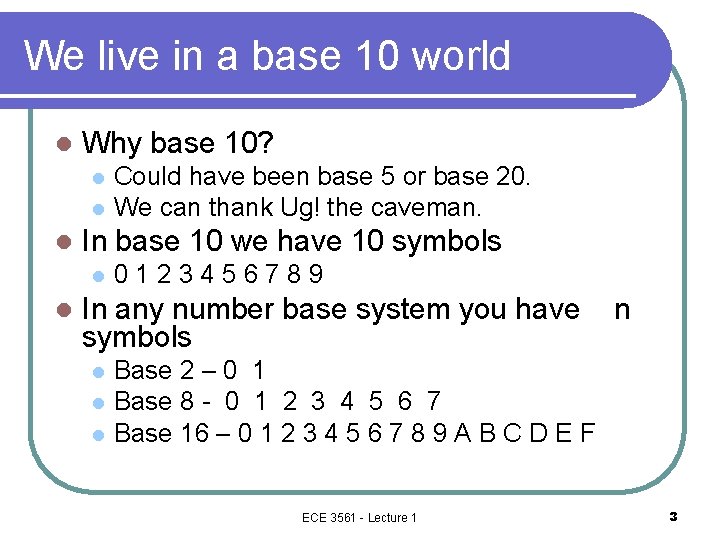
We live in a base 10 world l Why base 10? l l l In base 10 we have 10 symbols l l Could have been base 5 or base 20. We can thank Ug! the caveman. 0123456789 In any number base system you have symbols l l l n Base 2 – 0 1 Base 8 - 0 1 2 3 4 5 6 7 Base 16 – 0 1 2 3 4 5 6 7 8 9 A B C D E F ECE 3561 - Lecture 1 3
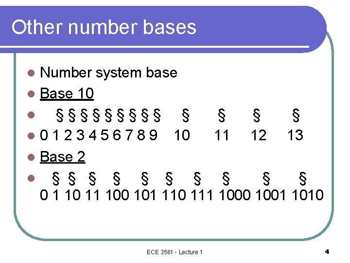
Other number bases Number system base l Base 10 l §§§§§ § § l 0 1 2 3 4 5 6 7 8 9 10 11 12 13 l Base 2 l § § § § § 0 1 10 11 100 101 110 111 1000 1001 1010 l ECE 3561 - Lecture 1 4

Base 5 and Base 8 l Base 5 (would have digits 0 to 4) §§§§ § § § l 0 1 2 3 4 10 11 12 13 14 20 21 l § § 22 23 l Base 8 (octal) l §§§§§§§ § § § l 0 1 2 3 4 5 6 7 10 11 12 13 14 15 ECE 3561 - Lecture 1 5

To and from base Base 10 to binary (base 2) Number in Base 10 1910 = ? Procedure (Integer division) l Divide by 2 19/2 = 9 r 1 l 9/2 = 4 r 1 l 4/2 = 2 r 0 l 2/2 = 1 r 0 l 1/ 2 = 0 r 1 l So the binary of 1910 is 1 0 0 1 1 l (In general for any number base you divide by the number system base and use the remainders) l More examples? l l ECE 3561 - Lecture 1 6
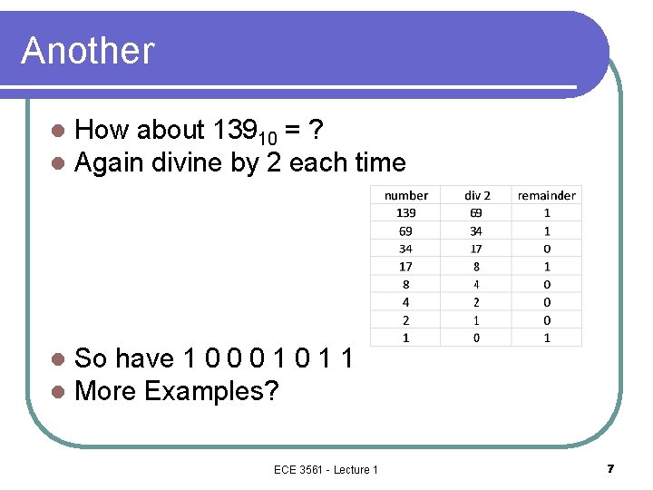
Another l l How about 13910 = ? Again divine by 2 each time l l So have 1 0 0 0 1 1 More Examples? ECE 3561 - Lecture 1 7
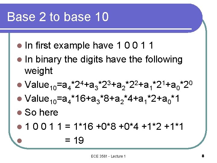
Base 2 to base 10 l In first example have 1 0 0 1 1 l In binary the digits have the following weight l Value 10=a 4*24+a 3*23+a 2*22+a 1*21+a 0*20 l Value 10=a 4*16+a 3*8+a 2*4+a 1*2+a 0*1 l So here l 1 0 0 1 1 = 1*16 +0*8 +0*4 +1*2 +1*1 l = 19 ECE 3561 - Lecture 1 8
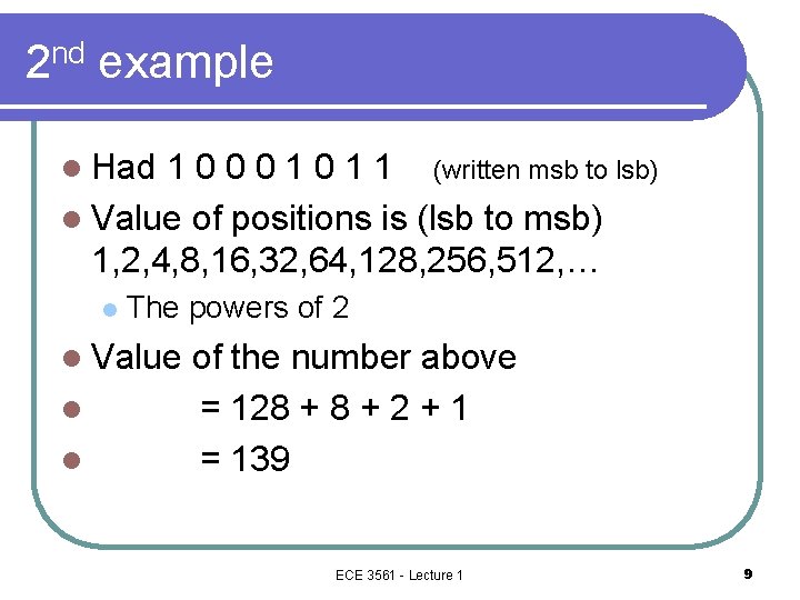
2 nd example l Had 1 0 0 0 1 1 (written msb to lsb) l Value of positions is (lsb to msb) 1, 2, 4, 8, 16, 32, 64, 128, 256, 512, … l The powers of 2 l Value l l of the number above = 128 + 2 + 1 = 139 ECE 3561 - Lecture 1 9
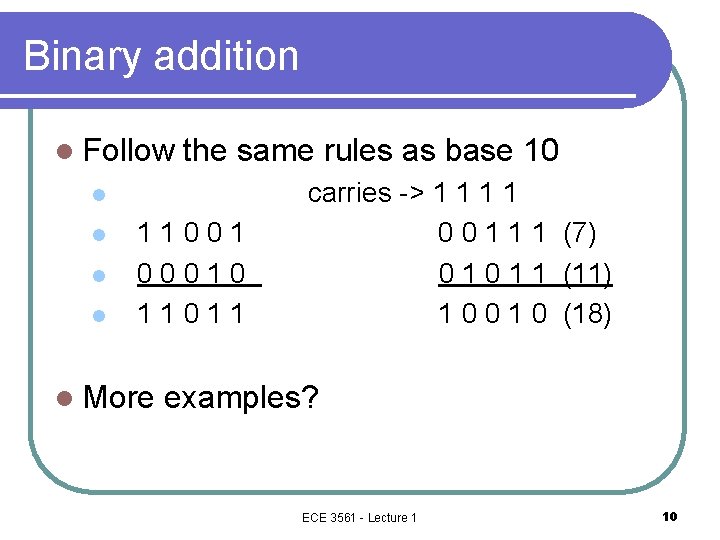
Binary addition l Follow the same rules as base 10 l l 11001 00010 11011 l More carries -> 1 1 0 0 1 1 1 (7) 0 1 1 (11) 1 0 0 1 0 (18) examples? ECE 3561 - Lecture 1 10
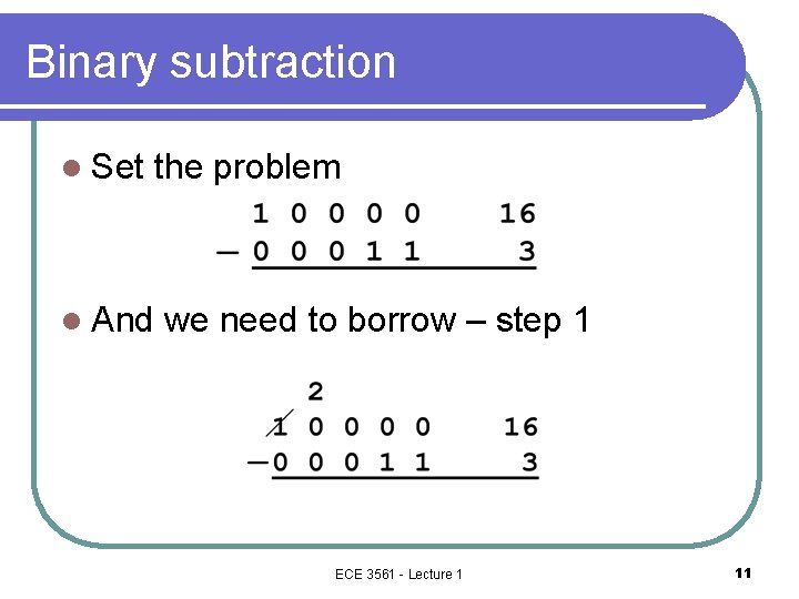
Binary subtraction l Set the problem l And we need to borrow – step 1 ECE 3561 - Lecture 1 11
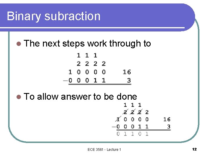
Binary subraction l The l To next steps work through to allow answer to be done ECE 3561 - Lecture 1 12

Binary multiplication l Just like multiplication in base 10 l More examples? ECE 3561 - Lecture 1 13
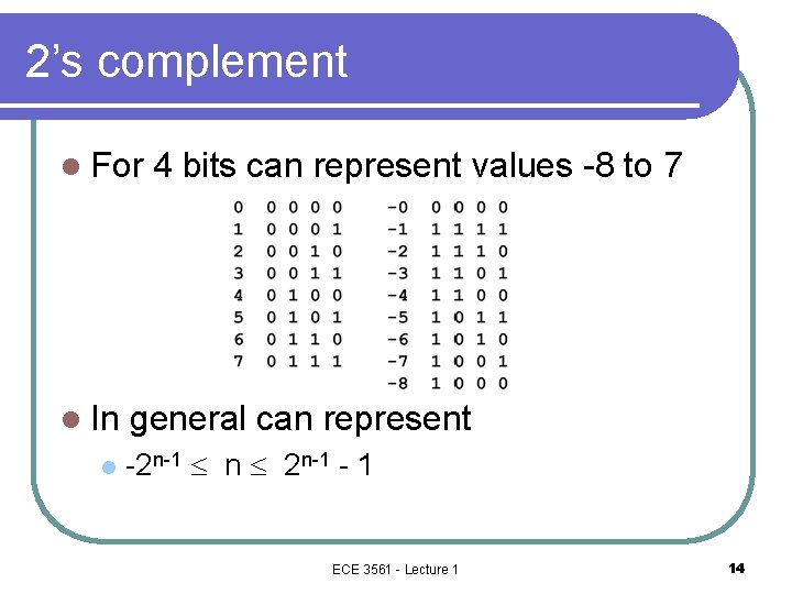
2’s complement l For l In l 4 bits can represent values -8 to 7 general can represent -2 n-1 £ n £ 2 n-1 - 1 ECE 3561 - Lecture 1 14
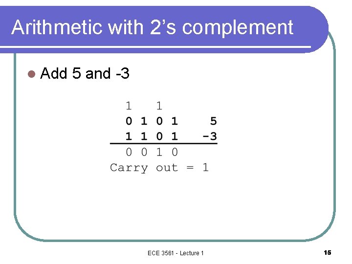
Arithmetic with 2’s complement l Add 5 and -3 ECE 3561 - Lecture 1 15
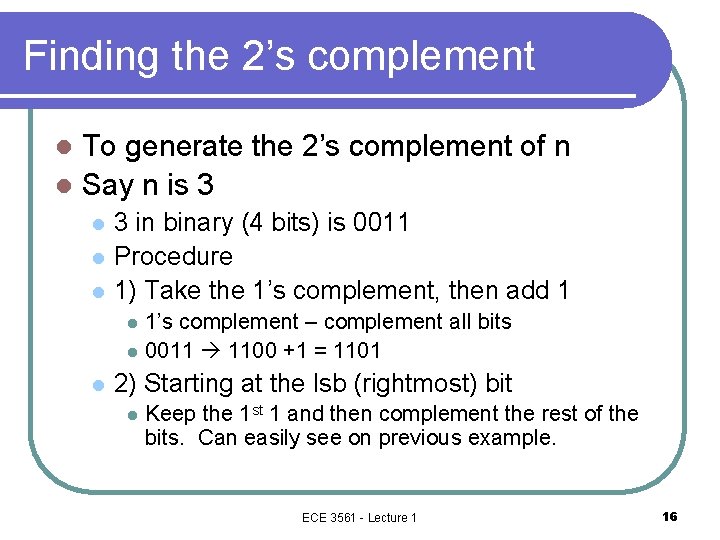
Finding the 2’s complement To generate the 2’s complement of n l Say n is 3 l l 3 in binary (4 bits) is 0011 Procedure 1) Take the 1’s complement, then add 1 l l l 1’s complement – complement all bits 0011 1100 +1 = 1101 2) Starting at the lsb (rightmost) bit l Keep the 1 st 1 and then complement the rest of the bits. Can easily see on previous example. ECE 3561 - Lecture 1 16
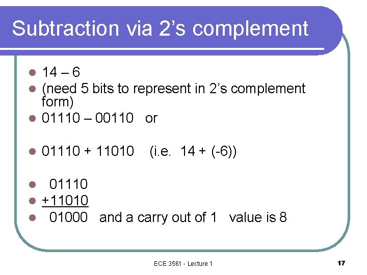
Subtraction via 2’s complement 14 – 6 (need 5 bits to represent in 2’s complement form) l 01110 – 00110 or l l l 01110 + 11010 (i. e. 14 + (-6)) l l l 01110 +11010 01000 and a carry out of 1 value is 8 ECE 3561 - Lecture 1 17
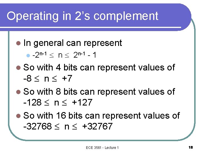
Operating in 2’s complement l In l general can represent -2 n-1 £ n £ 2 n-1 - 1 l So with 4 bits can represent values of -8 £ n £ +7 l So with 8 bits can represent values of -128 £ n £ +127 l So with 16 bits can represent values of -32768 £ n £ +32767 ECE 3561 - Lecture 1 18
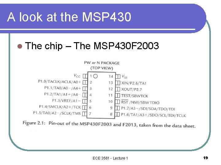
A look at the MSP 430 l The chip – The MSP 430 F 2003 ECE 3561 - Lecture 1 19
The pins l Vcc and Vss – Power and Ground being supplied to the chip. The data sheet specifies the tolerance on the voltage supply. l P 1. 0 -P 1. 7, P 2. 6, P 2. 7 are for digital input, grouped into 2 digital ports, P 1 and P 2 l TACLK, TA 0, TA 1 are associated with the Timer_A. More details to come. ECE 3561 - Lecture 1 20
The Pins (2) A 0 -, A 0+ up to A 4 - and A 4+ are inputs to the analog-to-digital converter. There are 4 channels and each has it own + and – input. Another pin, VREF is the reference voltage for the converter. l ACLK and SMCLK are outputs of clock signals and can be used to supply external devices with a clock. l XIN and XOUT are the connections for a crystal. l RST’ – is the active low reset signal (could also be designated _RST or /RST) l ECE 3561 - Lecture 1 21
The Pins (3) l NMI – the nonmaskable interrupt. Interrupts allow an external device to assert a value on this pin (a low) that causes the processor to halt operation after completion of the current instruction and ‘service’ the interrupt. When service is complete a software instruction allows resumption of normal operation. l There are no maskable interrupts ECE 3561 - Lecture 1 22
The Pins (4) TCK, TMS, TCLK, TD 1, TD 0 and TEST form the full JTAG interface used to program and debug the device. l SBWTDIO and SBWTCK provide the Spy. By-Wire interface which is an alternative to JTAG and uses only the 2 pins. l NOTE: each of the pins serves multiple purposes. The actual mode for each pin will vary across application and within a given application the use can be multiplexed. l ECE 3561 - Lecture 1 23
Assignment l l Read Chapter 1 and 2 READ FOR UNDERSTANDING l l l Bring your questions to class Assignments will be due 2 classes after assigned to the drop box on Carmen. No paper submissions – all are electronic. Next time – the internal structure of the MSP 430 and start assembler coding Go to ti. com – order launchpad – get Code Composer Studio Quiz next Monday at start of class. Go to wikipedia. com and read on von Neuman architecture. Write a 1 page summary and submit to drop box, HW 1 ECE 3561 - Lecture 1 24
- Slides: 24