ECE 232 Hardware Organization and Design 4 th
![Datapath: Register fields § Destination registers may differ across instruction formats: • R-format: [rd] Datapath: Register fields § Destination registers may differ across instruction formats: • R-format: [rd]](https://slidetodoc.com/presentation_image_h/03a47729791f031cdee22f38ea0ffce9/image-17.jpg)
- Slides: 32

ECE 232: Hardware Organization and Design 4 th Part 9: MIPS Lite edition: Chapter 4; 3 rd edition: Chapter 5 http: //www. ecs. umass. edu/ece 232/ Adapted from Computer Organization and Design, Patterson & Hennessy, UCB

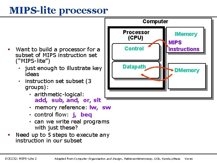
MIPS-lite processor Computer Processor (CPU) § § Want to build a processor for a subset of MIPS instruction set (“MIPS-lite”) • just enough to illustrate key ideas • instruction set subset (3 groups): • arithmetic-logical: add, sub, and, or, slt • memory reference: lw, sw • control flow: j, beq • can we write real programs with just these? Need up to 5 steps to execute any instruction in our subset ECE 232: MIPS-Lite 2 Control Datapath IMemory MIPS Instructions DMemory Adapted from Computer Organization and Design, Patterson&Hennessy, UCB, Kundu, UMass Koren

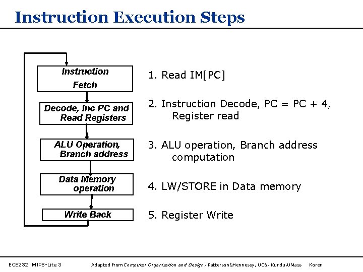
Instruction Execution Steps Instruction Fetch Decode, Inc PC and Read Registers ALU Operation, Branch address Data Memory operation Write Back ECE 232: MIPS-Lite 3 1. Read IM[PC] 2. Instruction Decode, PC = PC + 4, Register read 3. ALU operation, Branch address computation 4. LW/STORE in Data memory 5. Register Write Adapted from Computer Organization and Design, Patterson&Hennessy, UCB, Kundu, UMass Koren

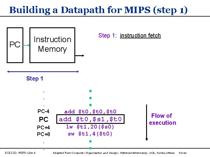
Building a Datapath for MIPS (step 1) PC Instruction Memory Step 1: instruction fetch Step 1. . . ECE 232: MIPS-Lite 4 PC-4 add $t 0, $t 0 PC add $t 0, $s 1, $t 0 PC+4 PC+8 lw $t 1, 20($s 0) sw $t 1, 4($t 0) . . Flow of execution Adapted from Computer Organization and Design, Patterson&Hennessy, UCB, Kundu, UMass Koren

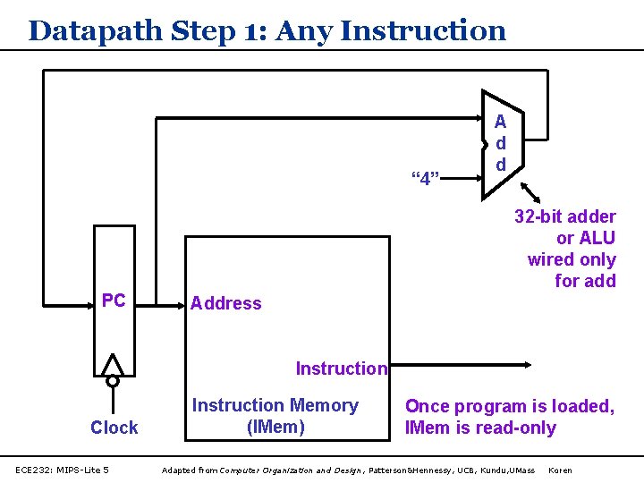
Datapath Step 1: Any Instruction “ 4” A d d 32 -bit adder or ALU wired only for add PC Address Instruction Clock ECE 232: MIPS-Lite 5 Instruction Memory (IMem) Once program is loaded, IMem is read-only Adapted from Computer Organization and Design, Patterson&Hennessy, UCB, Kundu, UMass Koren

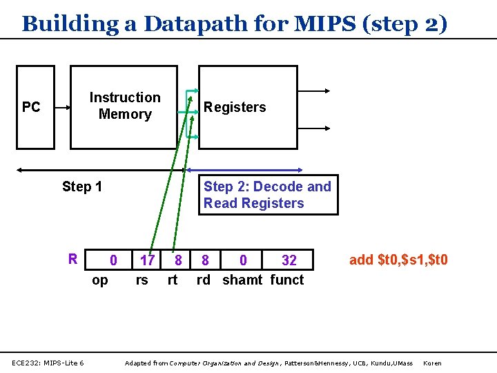
Building a Datapath for MIPS (step 2) Instruction Memory PC Step 1 R ECE 232: MIPS-Lite 6 Step 2: Decode and Read Registers 0 op Registers 17 8 rs rt 8 0 32 rd shamt funct add $t 0, $s 1, $t 0 Adapted from Computer Organization and Design, Patterson&Hennessy, UCB, Kundu, UMass Koren

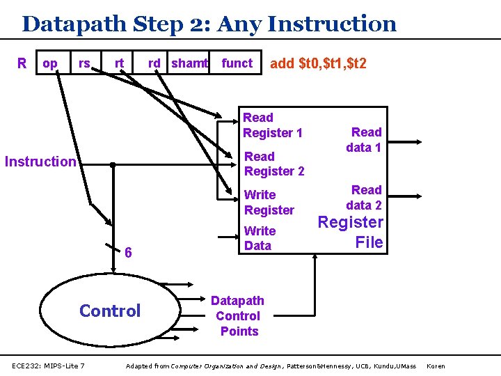
Datapath Step 2: Any Instruction R op rs rt rd shamt funct add $t 0, $t 1, $t 2 Read Register 1 Read Register 2 Instruction Write Register 6 Control ECE 232: MIPS-Lite 7 Write Data Read data 1 Read data 2 Register File Datapath Control Points Adapted from Computer Organization and Design, Patterson&Hennessy, UCB, Kundu, UMass Koren

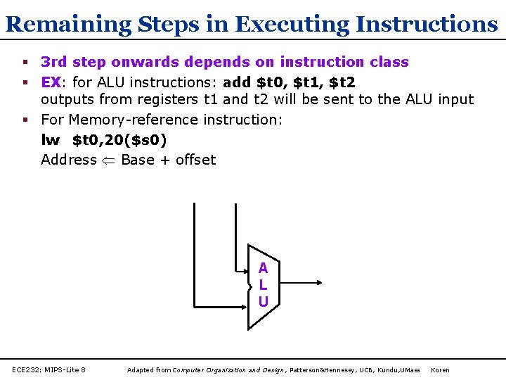
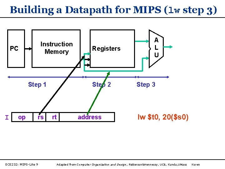
Remaining Steps in Executing Instructions § 3 rd step onwards depends on instruction class § EX: for ALU instructions: add $t 0, $t 1, $t 2 outputs from registers t 1 and t 2 will be sent to the ALU input § For Memory-reference instruction: lw $t 0, 20($s 0) Address Base + offset A L U ECE 232: MIPS-Lite 8 Adapted from Computer Organization and Design, Patterson&Hennessy, UCB, Kundu, UMass Koren

Building a Datapath for MIPS (lw step 3) Instruction Memory PC Step 1 I op rs ECE 232: MIPS-Lite 9 Registers Step 2 rt address A L U Step 3 lw $t 0, 20($s 0) Adapted from Computer Organization and Design, Patterson&Hennessy, UCB, Kundu, UMass Koren

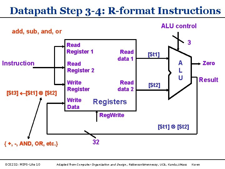
Datapath Step 3 -4: R-format Instructions ALU control add, sub, and, or 3 Read Register 1 Instruction Read data 1 Read Register 2 [$t 3] [$t 1] [$t 2] Write Register Write Data Read data 2 [$t 1] A L U [$t 2] Zero Result Registers Reg. Write [$t 1] [$t 2] { +, -, AND, OR, etc. } ECE 232: MIPS-Lite 10 32 Adapted from Computer Organization and Design, Patterson&Hennessy, UCB, Kundu, UMass Koren

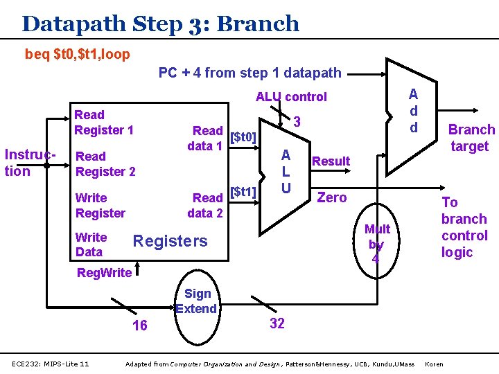
Datapath Step 3: Branch beq $t 0, $t 1, loop PC + 4 from step 1 datapath A d d ALU control Read Register 1 Instruction Read Register 2 Write Register Read [$t 0] data 1 Read data 2 Write Data [$t 1] 3 A L U Result Zero Mult by 4 Registers Branch target To branch control logic Reg. Write Sign Extend 16 ECE 232: MIPS-Lite 11 32 Adapted from Computer Organization and Design, Patterson&Hennessy, UCB, Kundu, UMass Koren

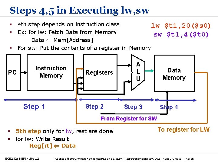
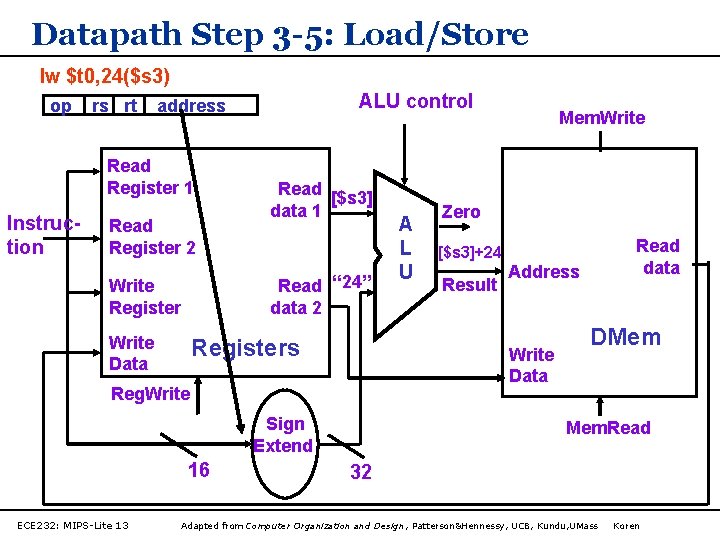
Steps 4, 5 in Executing lw, sw 4 th step depends on instruction class lw Ex: for lw: Fetch Data from Memory sw Data Mem[Address] For sw: Put the contents of a register in Memory § § § PC Instruction Memory Step 1 Registers Step 2 A L U Step 3 $t 1, 20($s 0) $t 1, 4($t 0) Data Memory Step 4 From Register for SW § § 5 th step only for lw; rest are done for lw: Write Result Reg[rt] Data ECE 232: MIPS-Lite 12 To register for LW Adapted from Computer Organization and Design, Patterson&Hennessy, UCB, Kundu, UMass Koren

Datapath Step 3 -5: Load/Store lw $t 0, 24($s 3) op rs rt Read Register 1 Instruction ALU control address Read Register 2 Read [$s 3] data 1 Read “ 24” data 2 Write Register Write Data Registers Sign Extend ECE 232: MIPS-Lite 13 Zero Read data [$s 3]+24 Result Address Write Data Reg. Write 16 A L U Mem. Write DMem Mem. Read 32 Adapted from Computer Organization and Design, Patterson&Hennessy, UCB, Kundu, UMass Koren

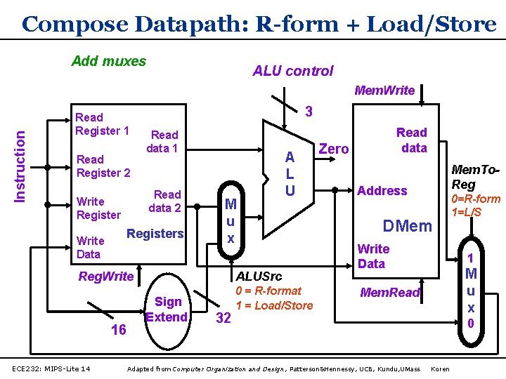
Compose Datapath: R-form + Load/Store Add muxes ALU control Instruction Mem. Write Read Register 1 Read Register 2 3 Read data 1 Read data 2 Write Registers Write Data M u x Reg. Write 16 ECE 232: MIPS-Lite 14 A L U ALUSrc Sign Extend 32 0 = R-format 1 = Load/Store Read data Zero Mem. To. Reg Address DMem Write Data 1 M u x Mem. Read Adapted from Computer Organization and Design, Patterson&Hennessy, UCB, Kundu, UMass 0=R-form 1=L/S 0 Koren

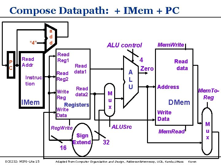
Compose Datapath: + IMem + PC “ 4” P C Read Addr Instruction IMem a d d ALU control Read Reg 1 Read Reg 2 Write Reg Read data 1 Read data 2 Registers Write Data A L U M u x ALUSrc Reg. Write 16 ECE 232: MIPS-Lite 15 Sign Extend Mem. Write 4 Zero Read data Address DMem Write Data M u x Mem. Read 32 Adapted from Computer Organization and Design, Patterson&Hennessy, UCB, Kundu, UMass Mem. To. Reg Koren

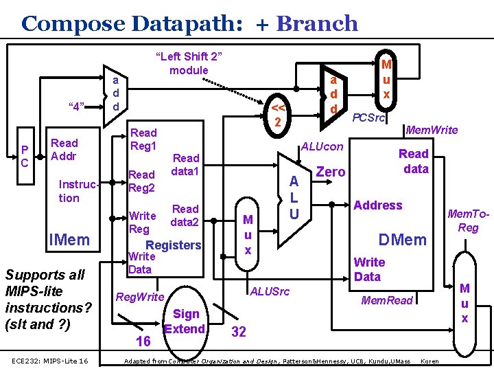
Compose Datapath: + Branch “ 4” P C Read Addr Instruction IMem Supports all MIPS-lite instructions? (slt and ? ) “Left Shift 2” module a d d Read Reg 1 Read Reg 2 Write Reg ECE 232: MIPS-Lite 16 << 2 Read data 2 Write Data M u x Mem. Write A L U ALUSrc Reg. Write Sign Extend PCSrc ALUcon Read data 1 Registers 16 a d d M u x Read data Zero Address DMem Write Data M u x Mem. Read 32 Adapted from Computer Organization and Design, Patterson&Hennessy, UCB, Kundu, UMass Mem. To. Reg Koren
![Datapath Register fields Destination registers may differ across instruction formats Rformat rd Datapath: Register fields § Destination registers may differ across instruction formats: • R-format: [rd]](https://slidetodoc.com/presentation_image_h/03a47729791f031cdee22f38ea0ffce9/image-17.jpg)
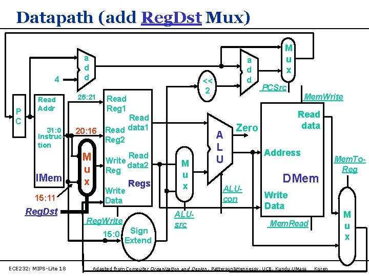
Datapath: Register fields § Destination registers may differ across instruction formats: • R-format: [rd] [rs] op [rt] add $t 0, $s 1 For this instruction, bits 11 -15 are the destination (t 0), which should be connected to the write reg. inputs • I-format: lw $t 0, 24($s 3) 6 bits 5 bits op rs rt rd 6 bits 5 bits shamt funct [rt] mem[[rs] + imm 16] 6 bits 5 bits 16 bits op rs rt offset For this instruction, bits 16 -20 should go to the write reg. port. Bits 0 -15 go to the ALU as address • Connection to the write reg. port changes! § Solution? mux to the rescue! ECE 232: MIPS-Lite 17 Adapted from Computer Organization and Design, Patterson&Hennessy, UCB, Kundu, UMass Koren

Datapath (add Reg. Dst Mux) 4 P C Read Addr 31: 0 Instruction IMem 15: 11 Reg. Dst a d d 25: 21 Read Reg 1 Read Write data 2 Reg Write Data Regs Reg. Write 15: 0 ECE 232: MIPS-Lite 18 << 2 Read 20: 16 Read data 1 Reg 2 M u x a d d Sign Extend M u x ALUsrc M u x PCSrc Mem. Write A L U Read data Zero ALUcon Address DMem Write Data M u x Mem. Read Adapted from Computer Organization and Design, Patterson&Hennessy, UCB, Kundu, UMass Mem. To. Reg Koren

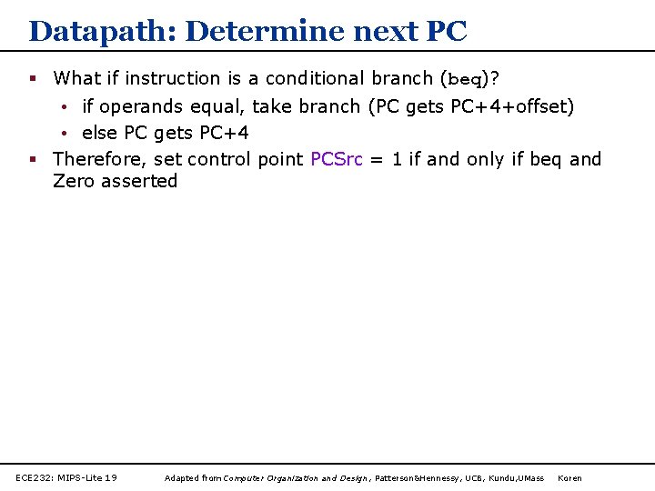
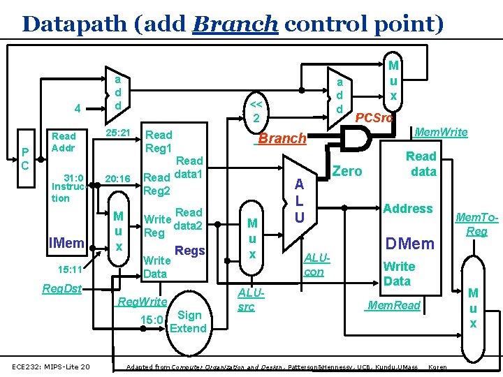
Datapath: Determine next PC § What if instruction is a conditional branch (beq)? • if operands equal, take branch (PC gets PC+4+offset) • else PC gets PC+4 § Therefore, set control point PCSrc = 1 if and only if beq and Zero asserted ECE 232: MIPS-Lite 19 Adapted from Computer Organization and Design, Patterson&Hennessy, UCB, Kundu, UMass Koren

Datapath (add Branch control point) 4 P C Read Addr 31: 0 Instruction IMem 15: 11 a d d << 2 25: 21 20: 16 M u x Read Reg 1 Read data 1 Reg 2 Read Write data 2 Reg Write Data Regs Reg. Write 15: 0 PCSrc Mem. Write Branch Reg. Dst ECE 232: MIPS-Lite 20 a d d M u x Sign Extend M u x ALUsrc A L U ALUcon Zero Read data Address DMem Write Data M u x Mem. Read Adapted from Computer Organization and Design, Patterson&Hennessy, UCB, Kundu, UMass Mem. To. Reg Koren

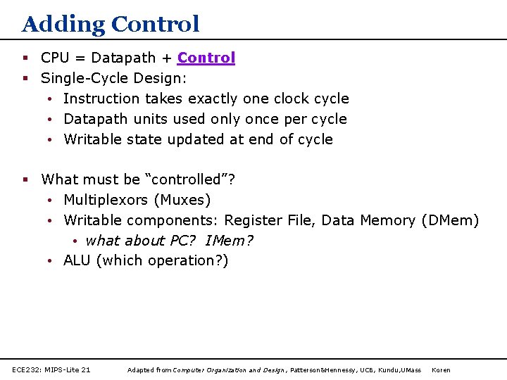
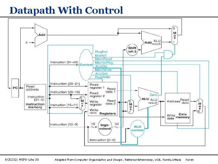
Adding Control § CPU = Datapath + Control § Single-Cycle Design: • Instruction takes exactly one clock cycle • Datapath units used only once per cycle • Writable state updated at end of cycle § What must be “controlled”? • Multiplexors (Muxes) • Writable components: Register File, Data Memory (DMem) • what about PC? IMem? • ALU (which operation? ) ECE 232: MIPS-Lite 21 Adapted from Computer Organization and Design, Patterson&Hennessy, UCB, Kundu, UMass Koren

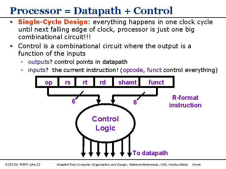
Processor = Datapath + Control § Single-Cycle Design: everything happens in one clock cycle until next falling edge of clock, processor is just one big combinational circuit!!! § Control is a combinational circuit where the output is a function of the inputs • outputs? control points in datapath • inputs? the current instruction! (opcode, funct control everything) op rs rt rd shamt 6 funct 6 R-format instruction Control Logic To datapath ECE 232: MIPS-Lite 22 Adapted from Computer Organization and Design, Patterson&Hennessy, UCB, Kundu, UMass Koren

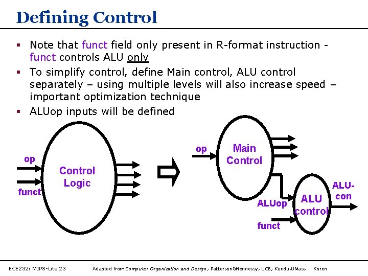
Defining Control § Note that funct field only present in R-format instruction funct controls ALU only § To simplify control, define Main control, ALU control separately – using multiple levels will also increase speed – important optimization technique § ALUop inputs will be defined op op funct Control Logic Main Control ALUop ALU control funct ECE 232: MIPS-Lite 23 Adapted from Computer Organization and Design, Patterson&Hennessy, UCB, Kundu, UMass Koren ALUcon

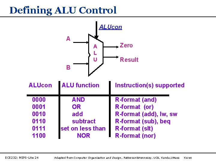
Defining ALU Control ALUcon A A L U Zero Result B ALUcon 0000 0001 0010 0111 1100 ECE 232: MIPS-Lite 24 ALU function Instruction(s) supported AND OR add subtract set on less than NOR R-format (and) R-format (or) R-format (add), lw, sw R-format (sub), beq R-format (slt) R-format (nor) Adapted from Computer Organization and Design, Patterson&Hennessy, UCB, Kundu, UMass Koren

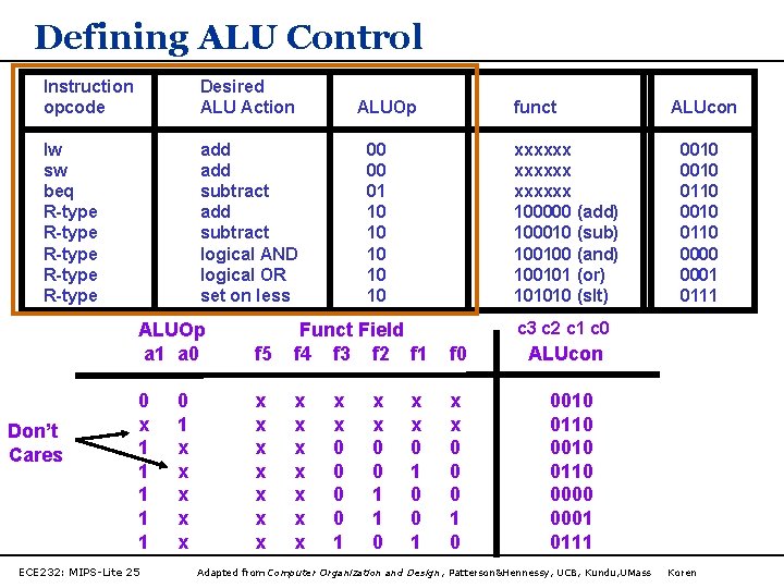
Defining ALU Control Instruction opcode Desired ALU Action lw sw beq R-type R-type add subtract logical AND logical OR set on less Don’t Cares ALUOp a 1 a 0 0 x 1 1 1 ECE 232: MIPS-Lite 25 0 1 x x x ALUOp funct 00 00 01 10 10 10 xxxxxx 100000 (add) 100010 (sub) 100100 (and) 100101 (or) 101010 (slt) f 5 f 0 x x x x 0 0 0 1 0 x x 0 0 1 1 0 x x 0 1 0010 0110 0001 0111 c 3 c 2 c 1 c 0 Funct Field f 4 f 3 f 2 f 1 x x 0 0 1 ALUcon 0010 0110 0000 0001 0111 Adapted from Computer Organization and Design, Patterson&Hennessy, UCB, Kundu, UMass Koren

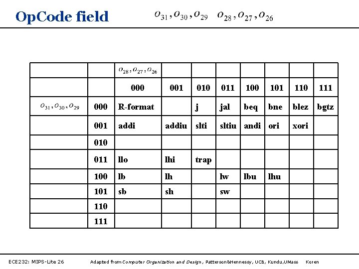
Op. Code field 000 001 010 011 100 101 110 j jal beq bne blez bgtz 000 R-format 001 addiu slti 011 llo lhi 100 lb lh lw 101 sb sh sw sltiu andi ori xori 010 trap lbu lhu 110 111 ECE 232: MIPS-Lite 26 Adapted from Computer Organization and Design, Patterson&Hennessy, UCB, Kundu, UMass Koren 111

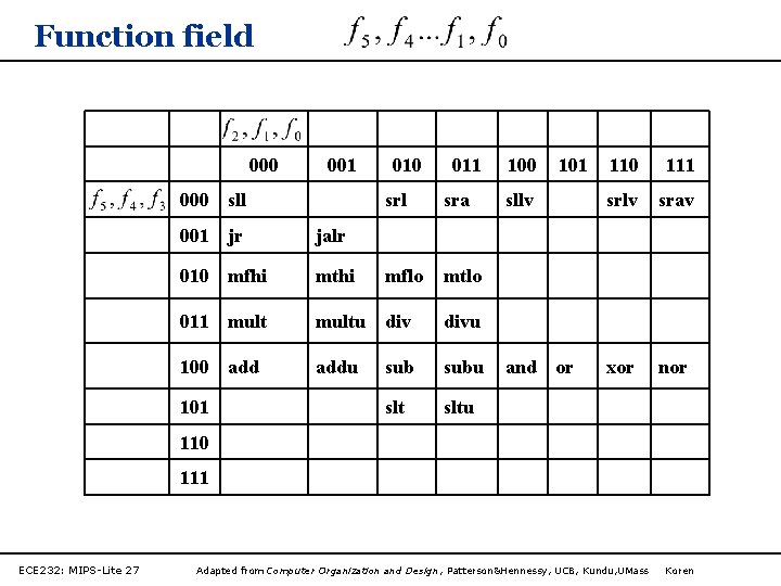
Function field 000 001 000 sll 010 011 srl sra 001 jr jalr 010 mfhi mthi mflo mtlo 011 multu divu 100 addu subu sltu 101 100 101 110 111 sllv srav and or xor nor 110 111 ECE 232: MIPS-Lite 27 Adapted from Computer Organization and Design, Patterson&Hennessy, UCB, Kundu, UMass Koren

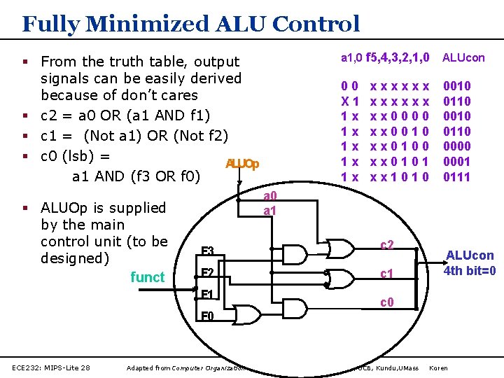
Fully Minimized ALU Control § From the truth table, output signals can be easily derived because of don’t cares § c 2 = a 0 OR (a 1 AND f 1) § c 1 = (Not a 1) OR (Not f 2) § c 0 (lsb) = ALUOp a 1 AND (f 3 OR f 0) § ALUOp is supplied by the main control unit (to be designed) funct ALUcon 00 X 1 1 x 1 x 1 x 0010 0110 0000 0001 0111 xxxxxx xx 0000 xx 0010 xx 0101 xx 1010 a 1 F 3 c 2 F 2 c 1 F 0 ECE 232: MIPS-Lite 28 a 1, 0 f 5, 4, 3, 2, 1, 0 ALUcon 4 th bit=0 c 0 Adapted from Computer Organization and Design, Patterson&Hennessy, UCB, Kundu, UMass Koren

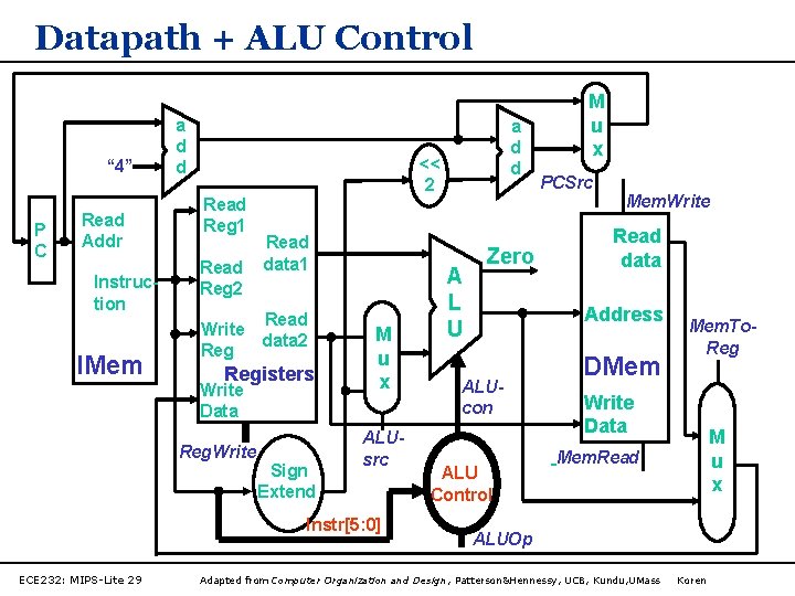
Datapath + ALU Control “ 4” P C Read Addr Instruction IMem a d d Read Reg 1 Read Reg 2 << 2 Read data 1 Read Write data 2 Registers Write Data Reg. Write Sign Extend M u x ALUsrc Instr[5: 0] ECE 232: MIPS-Lite 29 a d d A L U Zero M u x PCSrc Mem. Write Read data Address ALUcon ALU Control DMem Mem. To. Reg Write Data M u x Mem. Read ALUOp Adapted from Computer Organization and Design, Patterson&Hennessy, UCB, Kundu, UMass Koren

Datapath With Control ECE 232: MIPS-Lite 30 Adapted from Computer Organization and Design, Patterson&Hennessy, UCB, Kundu, UMass Koren

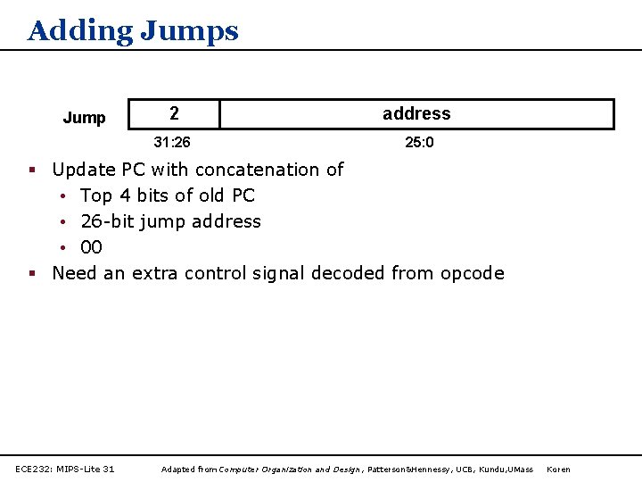
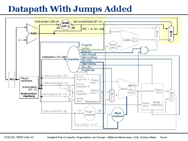
Adding Jumps Jump 2 address 31: 26 25: 0 § Update PC with concatenation of • Top 4 bits of old PC • 26 -bit jump address • 00 § Need an extra control signal decoded from opcode ECE 232: MIPS-Lite 31 Adapted from Computer Organization and Design, Patterson&Hennessy, UCB, Kundu, UMass Koren

Datapath With Jumps Added ECE 232: MIPS-Lite 32 Adapted from Computer Organization and Design, Patterson&Hennessy, UCB, Kundu, UMass Koren