ECE 152 496 Introduction to Computer Architecture Caches
![Full-Associativity 0 1 == 1022 == [31: 2] 1023 == 1: 0 == << Full-Associativity 0 1 == 1022 == [31: 2] 1023 == 1: 0 == <<](https://slidetodoc.com/presentation_image_h2/bf27db5bf64566f7c1e8645616ea5c93/image-45.jpg)
- Slides: 67

ECE 152 / 496 Introduction to Computer Architecture Caches and Memory Hierarchies Benjamin C. Lee Duke University Slides from Daniel Sorin (Duke) and are derived from work by Amir Roth (Penn) and Alvy Lebeck (Duke) 1

Where We Are in This Course Right Now • So far: • We know how to design a processor that can fetch, decode, and execute the instructions in an ISA • We have assumed that memory storage (for instructions and data) is a magic black box • Now: • We learn why memory storage systems are hierarchical • We learn about caches and SRAM technology for caches • Next: • We learn how to implement main memory © 2012 Daniel J. Sorin from Roth and Lebeck ECE 152 2

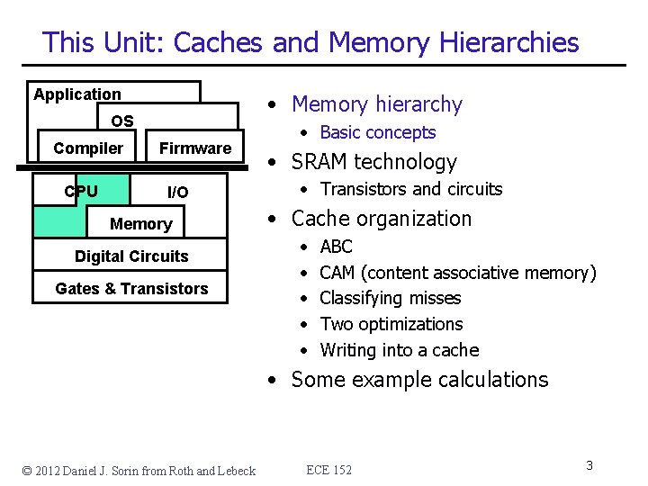
This Unit: Caches and Memory Hierarchies Application • Memory hierarchy OS Compiler CPU Firmware I/O Memory Digital Circuits Gates & Transistors • Basic concepts • SRAM technology • Transistors and circuits • Cache organization • • • ABC CAM (content associative memory) Classifying misses Two optimizations Writing into a cache • Some example calculations © 2012 Daniel J. Sorin from Roth and Lebeck ECE 152 3

Readings • Patterson and Hennessy • Chapter 5 © 2012 Daniel J. Sorin from Roth and Lebeck ECE 152 4

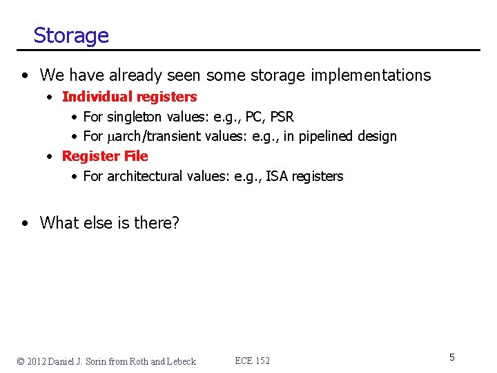
Storage • We have already seen some storage implementations • Individual registers • For singleton values: e. g. , PC, PSR • For march/transient values: e. g. , in pipelined design • Register File • For architectural values: e. g. , ISA registers • What else is there? © 2012 Daniel J. Sorin from Roth and Lebeck ECE 152 5

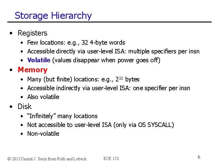
Storage Hierarchy • Registers • Few locations: e. g. , 32 4 -byte words • Accessible directly via user-level ISA: multiple specifiers per insn • Volatile (values disappear when power goes off) • Memory • Many (but finite) locations: e. g. , 232 bytes • Accessible indirectly via user-level ISA: one specifier per insn • Also volatile • Disk • “Infinitely” many locations • Not accessible to user-level ISA (only via OS SYSCALL) • Non-volatile © 2012 Daniel J. Sorin from Roth and Lebeck ECE 152 6

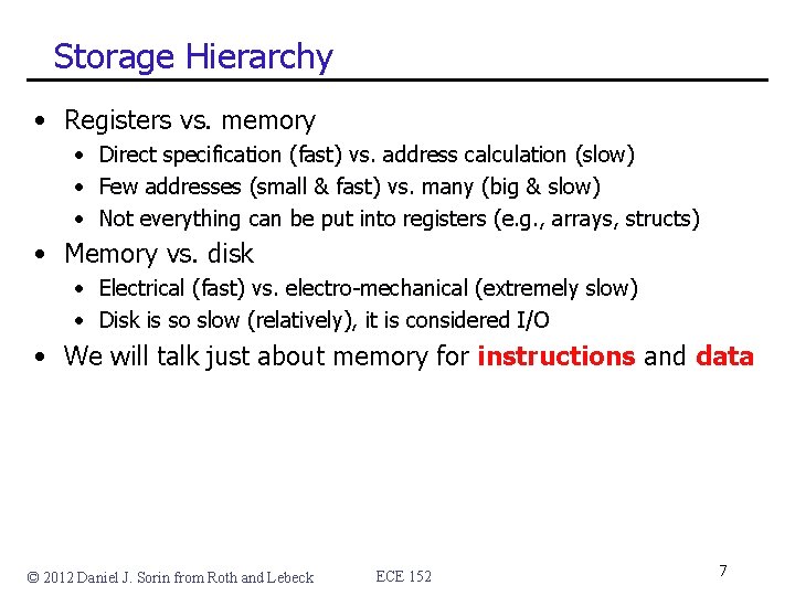
Storage Hierarchy • Registers vs. memory • Direct specification (fast) vs. address calculation (slow) • Few addresses (small & fast) vs. many (big & slow) • Not everything can be put into registers (e. g. , arrays, structs) • Memory vs. disk • Electrical (fast) vs. electro-mechanical (extremely slow) • Disk is so slow (relatively), it is considered I/O • We will talk just about memory for instructions and data © 2012 Daniel J. Sorin from Roth and Lebeck ECE 152 7

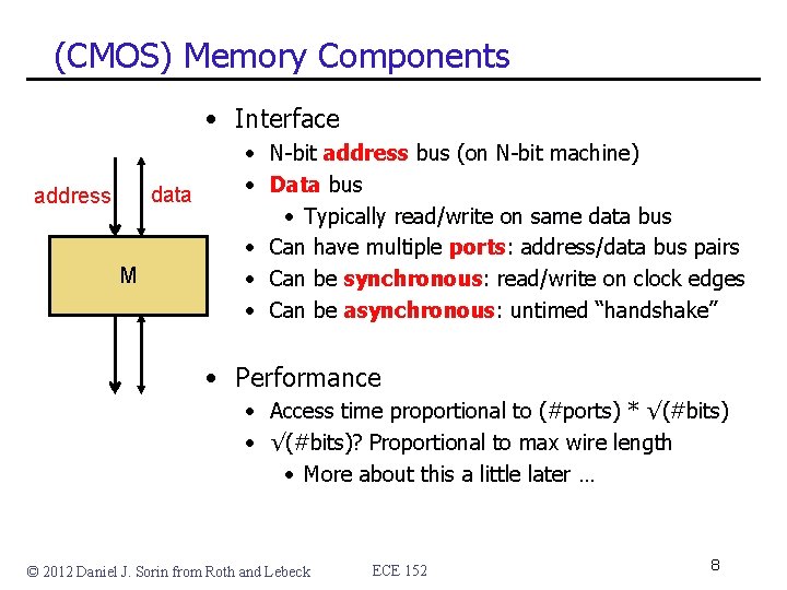
(CMOS) Memory Components • Interface data address M • N-bit address bus (on N-bit machine) • Data bus • Typically read/write on same data bus • Can have multiple ports: address/data bus pairs • Can be synchronous: read/write on clock edges • Can be asynchronous: untimed “handshake” • Performance • Access time proportional to (#ports) * √(#bits) • √(#bits)? Proportional to max wire length • More about this a little later … © 2012 Daniel J. Sorin from Roth and Lebeck ECE 152 8

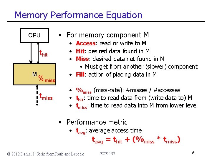
Memory Performance Equation CPU thit M %miss tmiss • For memory component M • Access: read or write to M • Hit: desired data found in M • Miss: desired data not found in M • Must get from another (slower) component • Fill: action of placing data in M • %miss (miss-rate): #misses / #accesses • thit: time to read data from (write data to) M • tmiss: time to read data into M from lower level • Performance metric • tavg: average access time tavg = thit + (%miss * tmiss) © 2012 Daniel J. Sorin from Roth and Lebeck ECE 152 9

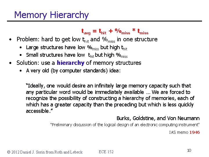
Memory Hierarchy tavg = thit + %miss * tmiss • Problem: hard to get low thit and %miss in one structure • Large structures have low %miss but high thit • Small structures have low thit but high %miss • Solution: use a hierarchy of memory structures • A very old (by computer standards) idea: “Ideally, one would desire an infinitely large memory capacity such that any particular word would be immediately available … We are forced to recognize the possibility of constructing a hierarchy of memories, each of which has a greater capacity than the preceding but which is less quickly accessible. ” Burks, Goldstine, and Von Neumann “Preliminary discussion of the logical design of an electronic computing instrument” IAS memo 1946 © 2012 Daniel J. Sorin from Roth and Lebeck ECE 152 10

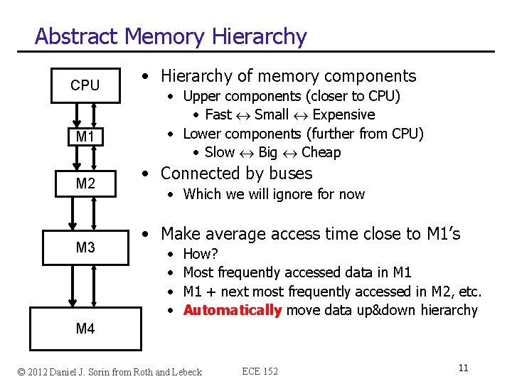
Abstract Memory Hierarchy CPU M 1 M 2 M 3 • Hierarchy of memory components • Upper components (closer to CPU) • Fast Small Expensive • Lower components (further from CPU) • Slow Big Cheap • Connected by buses • Which we will ignore for now • Make average access time close to M 1’s • • How? Most frequently accessed data in M 1 + next most frequently accessed in M 2, etc. Automatically move data up&down hierarchy M 4 © 2012 Daniel J. Sorin from Roth and Lebeck ECE 152 11

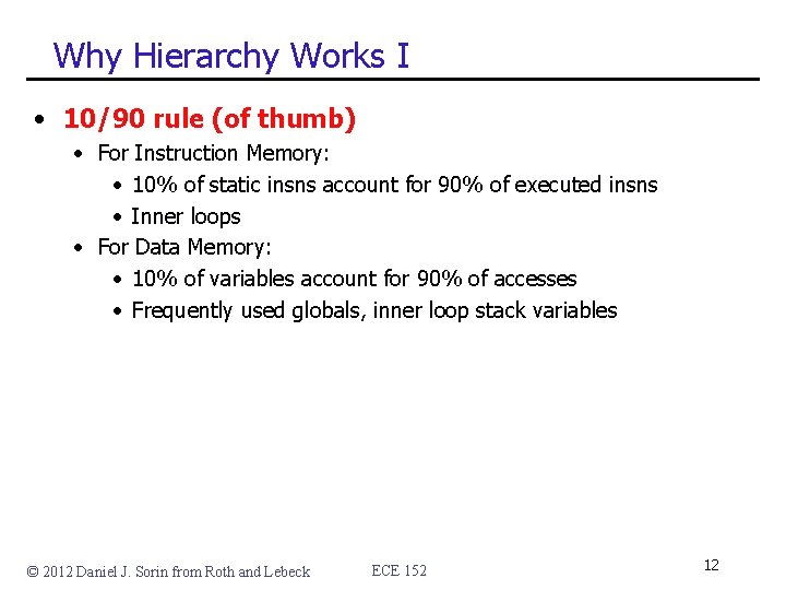
Why Hierarchy Works I • 10/90 rule (of thumb) • For Instruction Memory: • 10% of static insns account for 90% of executed insns • Inner loops • For Data Memory: • 10% of variables account for 90% of accesses • Frequently used globals, inner loop stack variables © 2012 Daniel J. Sorin from Roth and Lebeck ECE 152 12

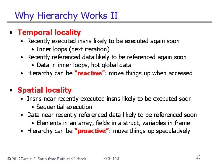
Why Hierarchy Works II • Temporal locality • Recently executed insns likely to be executed again soon • Inner loops (next iteration) • Recently referenced data likely to be referenced again soon • Data in inner loops, hot global data • Hierarchy can be “reactive”: move things up when accessed • Spatial locality • Insns near recently executed insns likely to be executed soon • Sequential execution • Data near recently referenced data likely to be referenced soon • Elements in an array, fields in a struct, variables in frame • Hierarchy can be “proactive”: move things up speculatively © 2012 Daniel J. Sorin from Roth and Lebeck ECE 152 13

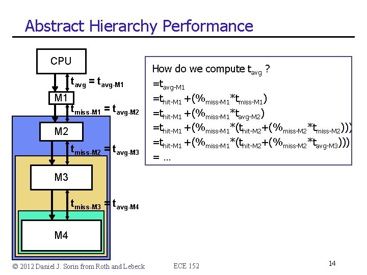
Abstract Hierarchy Performance CPU tavg = tavg-M 1 tmiss-M 1 = tavg-M 2 tmiss-M 2 = tavg-M 3 How do we compute tavg ? =tavg-M 1 =thit-M 1 +(%miss-M 1*tmiss-M 1) =thit-M 1 +(%miss-M 1*tavg-M 2) =thit-M 1 +(%miss-M 1*(thit-M 2+(%miss-M 2*tmiss-M 2))) =thit-M 1 +(%miss-M 1*(thit-M 2+(%miss-M 2*tavg-M 3))) =… M 3 tmiss-M 3 = tavg-M 4 © 2012 Daniel J. Sorin from Roth and Lebeck ECE 152 14

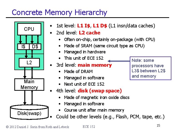
Concrete Memory Hierarchy CPU I$ D$ L 2 Main Memory Disk(swap) • 1 st level: L 1 I$, L 1 D$ (L 1 insn/data caches) • 2 nd level: L 2 cache • • Often on-chip, certainly on-package (with CPU) Made of SRAM (same circuit type as CPU) Managed in hardware This unit of ECE 152 Note: some • 3 rd level: main memory • Made of DRAM • Managed in software • Next unit of ECE 152 processors have L 3$ between L 2$ and memory • 4 th level: disk (swap space) • Made of magnetic iron oxide discs • Managed in software • Course unit after main memory • Could be other levels (e. g. , Flash, PCM, tape, etc. ) © 2012 Daniel J. Sorin from Roth and Lebeck ECE 152 15

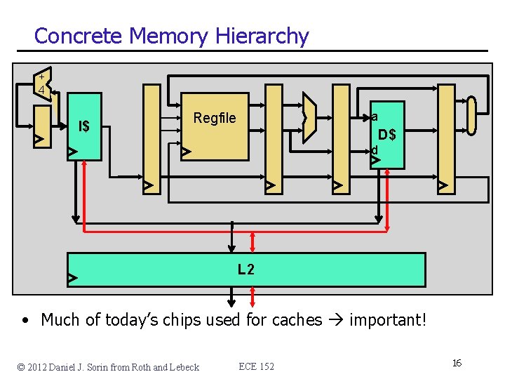
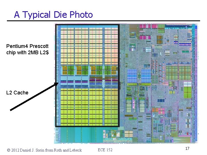
Concrete Memory Hierarchy + 4 I$ a Regfile D$ d L 2 • Much of today’s chips used for caches important! © 2012 Daniel J. Sorin from Roth and Lebeck ECE 152 16

A Typical Die Photo Pentium 4 Prescott chip with 2 MB L 2$ L 2 Cache © 2012 Daniel J. Sorin from Roth and Lebeck ECE 152 17

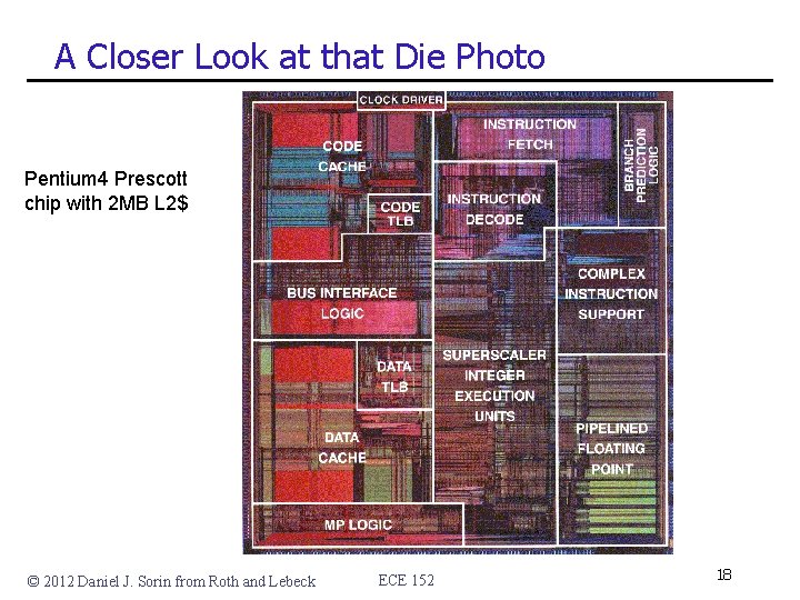
A Closer Look at that Die Photo Pentium 4 Prescott chip with 2 MB L 2$ © 2012 Daniel J. Sorin from Roth and Lebeck ECE 152 18

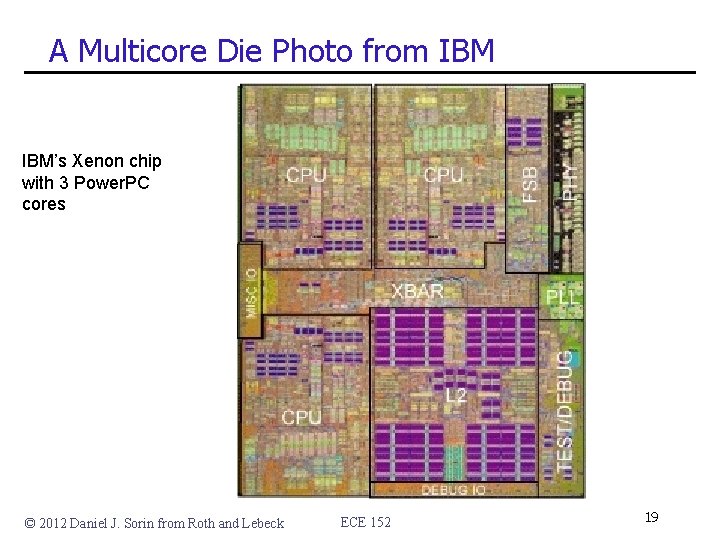
A Multicore Die Photo from IBM’s Xenon chip with 3 Power. PC cores © 2012 Daniel J. Sorin from Roth and Lebeck ECE 152 19

This Unit: Caches and Memory Hierarchies Application • Memory hierarchy OS Compiler CPU Firmware I/O Memory Digital Circuits Gates & Transistors • Basic concepts • SRAM technology • Transistors and circuits • Cache organization • • • ABC CAM (content associative memory) Classifying misses Two optimizations Writing into a cache • Some example calculations © 2012 Daniel J. Sorin from Roth and Lebeck ECE 152 20

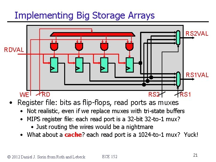
Implementing Big Storage Arrays RS 2 VAL RDVAL RS 1 VAL WE RD RS 2 • Register file: bits as flip-flops, read ports as muxes RS 1 • Not realistic, even if we replace muxes with tri-state buffers • MIPS register file: each read port is a 32 -bit 32 -to-1 mux? • Just routing the wires would be a nightmare • What about a cache? each read port is a 1024 -to-1 mux? Yuck! © 2012 Daniel J. Sorin from Roth and Lebeck ECE 152 21

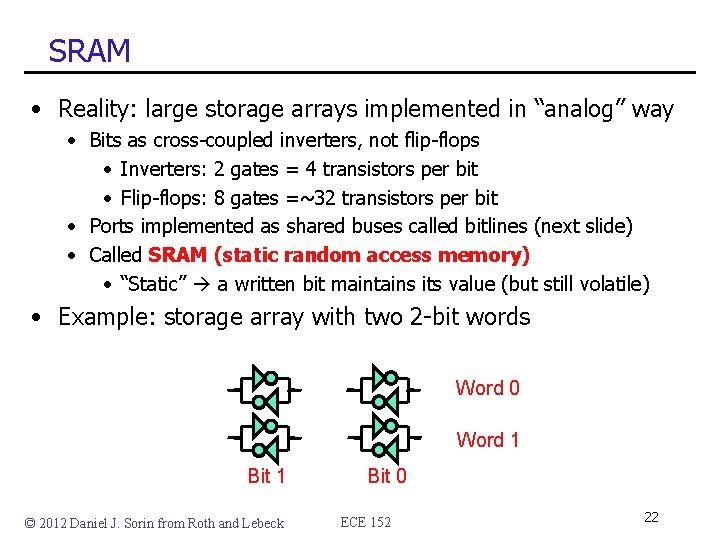
SRAM • Reality: large storage arrays implemented in “analog” way • Bits as cross-coupled inverters, not flip-flops • Inverters: 2 gates = 4 transistors per bit • Flip-flops: 8 gates =~32 transistors per bit • Ports implemented as shared buses called bitlines (next slide) • Called SRAM (static random access memory) • “Static” a written bit maintains its value (but still volatile) • Example: storage array with two 2 -bit words Word 0 Word 1 Bit 1 © 2012 Daniel J. Sorin from Roth and Lebeck Bit 0 ECE 152 22

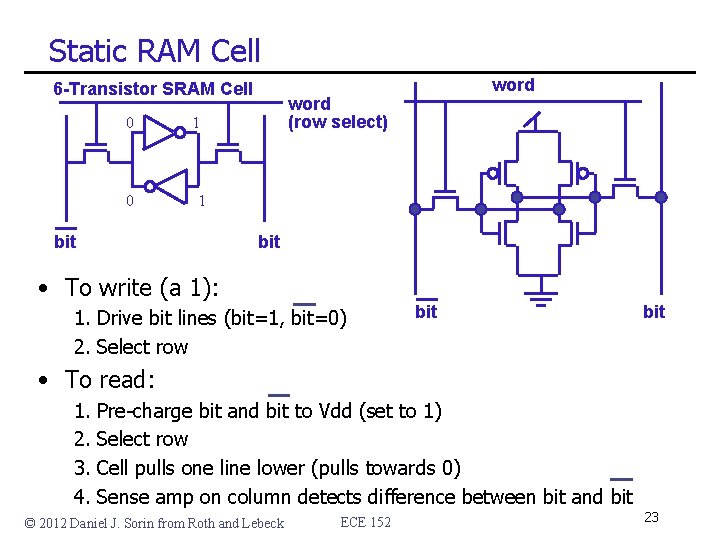
Static RAM Cell 6 -Transistor SRAM Cell 0 0 word (row select) 1 1 bit • To write (a 1): 1. Drive bit lines (bit=1, bit=0) 2. Select row bit • To read: 1. 2. 3. 4. Pre-charge bit and bit to Vdd (set to 1) Select row Cell pulls one line lower (pulls towards 0) Sense amp on column detects difference between bit and bit © 2012 Daniel J. Sorin from Roth and Lebeck ECE 152 23

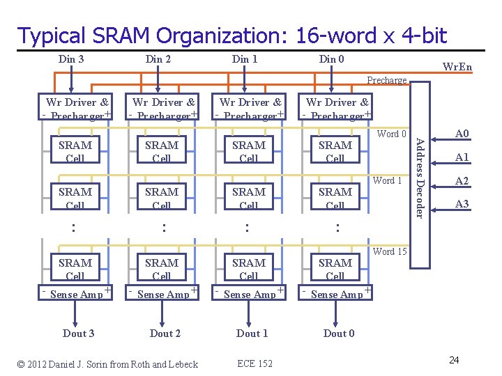
Typical SRAM Organization: 16 -word x 4 -bit Din 3 Din 2 Din 1 Din 0 Wr. En Precharge Wr Driver & - Precharger+ SRAM Cell SRAM Cell : : SRAM Cell - Sense Amp + Dout 3 Dout 2 Dout 1 Dout 0 © 2012 Daniel J. Sorin from Roth and Lebeck ECE 152 Word 0 Word 1 Address Decoder SRAM Cell Wr Driver & - Precharger+ A 0 A 1 A 2 A 3 Word 15 24

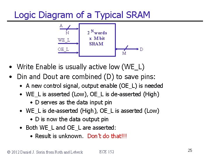
Logic Diagram of a Typical SRAM A N WE_L 2 N words x M bit SRAM OE_L M D • Write Enable is usually active low (WE_L) • Din and Dout are combined (D) to save pins: • A new control signal, output enable (OE_L) is needed • WE_L is asserted (Low), OE_L is de-asserted (High) • D serves as the data input pin • WE_L is de-asserted (High), OE_L is asserted (Low) • D is now the data output pin • Both WE_L and OE_L are asserted: • Result is unknown. Don’t do that!!! © 2012 Daniel J. Sorin from Roth and Lebeck ECE 152 25

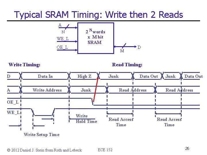
Typical SRAM Timing: Write then 2 Reads A 2 N words x M bit SRAM N WE_L OE_L M Write Timing: D A Data In Write Address D Read Timing: High Z Junk Data Out Read Address OE_L Write Hold Time Read Access Time Write Setup Time © 2012 Daniel J. Sorin from Roth and Lebeck ECE 152 26

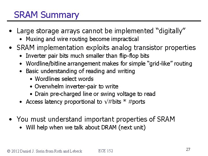
SRAM Summary • Large storage arrays cannot be implemented “digitally” • Muxing and wire routing become impractical • SRAM implementation exploits analog transistor properties • Inverter pair bits much smaller than flip-flop bits • Wordline/bitline arrangement makes for simple “grid-like” routing • Basic understanding of reading and writing • Wordlines select words • Overwhelm inverter-pair to write • Drain pre-charged line or swing voltage to read • Access latency proportional to √#bits * #ports • You must understand important properties of SRAM • Will help when we talk about DRAM (next unit) © 2012 Daniel J. Sorin from Roth and Lebeck ECE 152 27

This Unit: Caches and Memory Hierarchies Application • Memory hierarchy OS Compiler CPU Firmware I/O Memory Digital Circuits Gates & Transistors • Basic concepts • SRAM technology • Transistors and circuits • Cache organization • • • ABCs CAM (content associative memory) Classifying misses Two optimizations Writing into a cache • Some example calculations © 2012 Daniel J. Sorin from Roth and Lebeck ECE 152 28

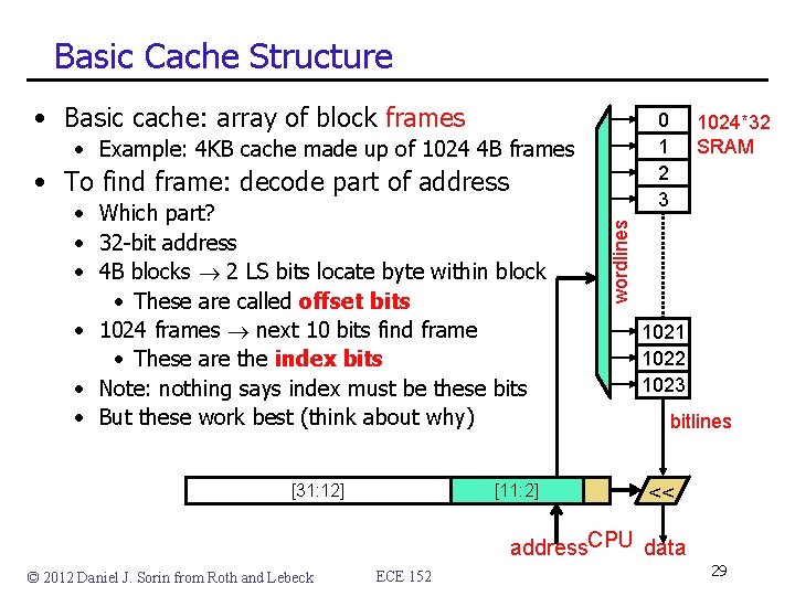
Basic Cache Structure • Basic cache: array of block frames 0 1 2 3 • Example: 4 KB cache made up of 1024 4 B frames • Which part? • 32 -bit address • 4 B blocks 2 LS bits locate byte within block • These are called offset bits • 1024 frames next 10 bits find frame • These are the index bits • Note: nothing says index must be these bits • But these work best (think about why) [31: 12] [11: 2] wordlines • To find frame: decode part of address 1024*32 SRAM 1021 1022 1023 bitlines << address. CPU data © 2012 Daniel J. Sorin from Roth and Lebeck ECE 152 29

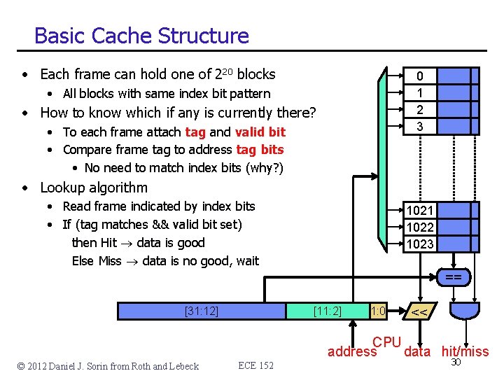
Basic Cache Structure • Each frame can hold one of 220 blocks 0 1 2 3 • All blocks with same index bit pattern • How to know which if any is currently there? • To each frame attach tag and valid bit • Compare frame tag to address tag bits • No need to match index bits (why? ) • Lookup algorithm • Read frame indicated by index bits • If (tag matches && valid bit set) then Hit data is good Else Miss data is no good, wait 1021 1022 1023 == [31: 12] [11: 2] 1: 0 << CPU address data hit/miss © 2012 Daniel J. Sorin from Roth and Lebeck ECE 152 30

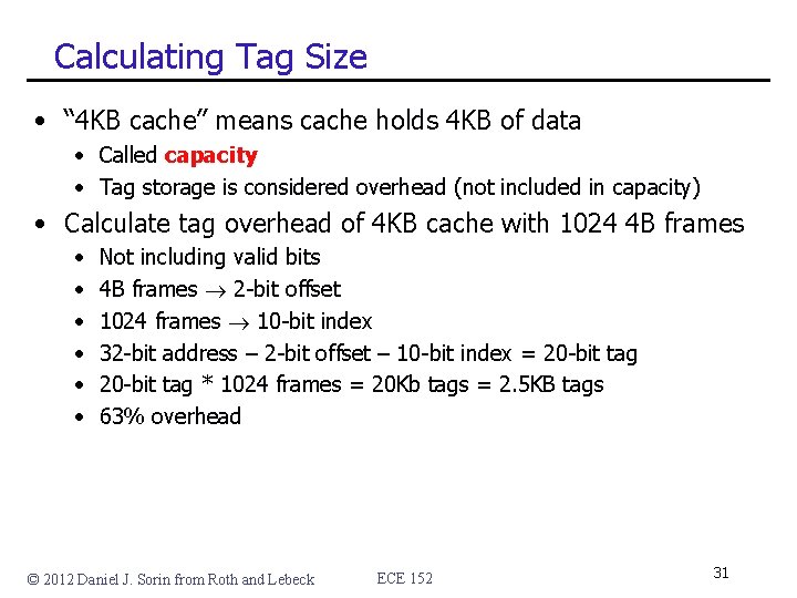
Calculating Tag Size • “ 4 KB cache” means cache holds 4 KB of data • Called capacity • Tag storage is considered overhead (not included in capacity) • Calculate tag overhead of 4 KB cache with 1024 4 B frames • • • Not including valid bits 4 B frames 2 -bit offset 1024 frames 10 -bit index 32 -bit address – 2 -bit offset – 10 -bit index = 20 -bit tag * 1024 frames = 20 Kb tags = 2. 5 KB tags 63% overhead © 2012 Daniel J. Sorin from Roth and Lebeck ECE 152 31

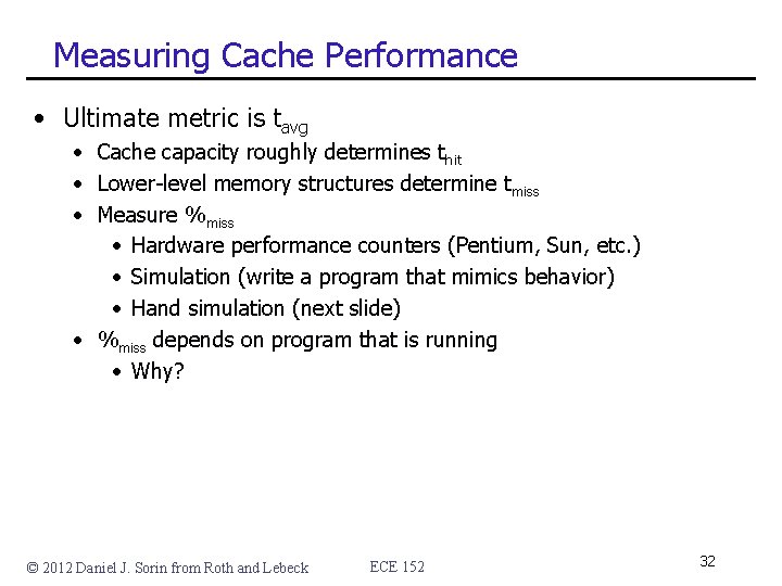
Measuring Cache Performance • Ultimate metric is tavg • Cache capacity roughly determines thit • Lower-level memory structures determine tmiss • Measure %miss • Hardware performance counters (Pentium, Sun, etc. ) • Simulation (write a program that mimics behavior) • Hand simulation (next slide) • %miss depends on program that is running • Why? © 2012 Daniel J. Sorin from Roth and Lebeck ECE 152 32

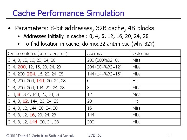
Cache Performance Simulation • Parameters: 8 -bit addresses, 32 B cache, 4 B blocks • Addresses initially in cache : 0, 4, 8, 12, 16, 20, 24, 28 • To find location in cache, do mod 32 arithmetic (why 32? ) Cache contents (prior to access) Address Outcome 0, 4, 8, 12, 16, 20, 24, 28 200 (200%32=8) Miss 0, 4, 200, 12, 16, 20, 24, 28 204 (204%32=12) Miss 0, 4, 200, 204, 16, 20, 24, 28 144 (144%32=16) Miss 0, 4, 200, 204, 144, 20, 24, 28 6 Hit 0, 4, 200, 204, 144, 20, 24, 28 8 Miss 0, 4, 8, 204, 144, 20, 24, 28 12 Miss 0, 4, 8, 12, 144, 20, 24, 28 20 Hit 0, 4, 8, 12, 144, 20, 24, 28 16 Miss 0, 4, 8, 12, 16, 20, 24, 28 144 Miss 0, 4, 8, 12, 144, 20, 24, 28 200 Miss © 2012 Daniel J. Sorin from Roth and Lebeck ECE 152 33

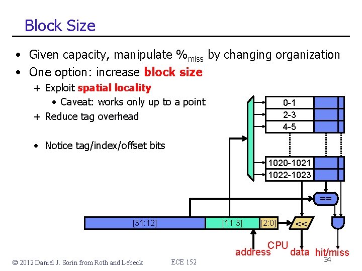
Block Size • Given capacity, manipulate %miss by changing organization • One option: increase block size + Exploit spatial locality • Caveat: works only up to a point + Reduce tag overhead 0 -1 2 -3 4 -5 • Notice tag/index/offset bits 1020 -1021 1022 -1023 == [31: 12] © 2012 Daniel J. Sorin from Roth and Lebeck [11: 3] ECE 152 [2: 0] << CPU address data hit/miss 34

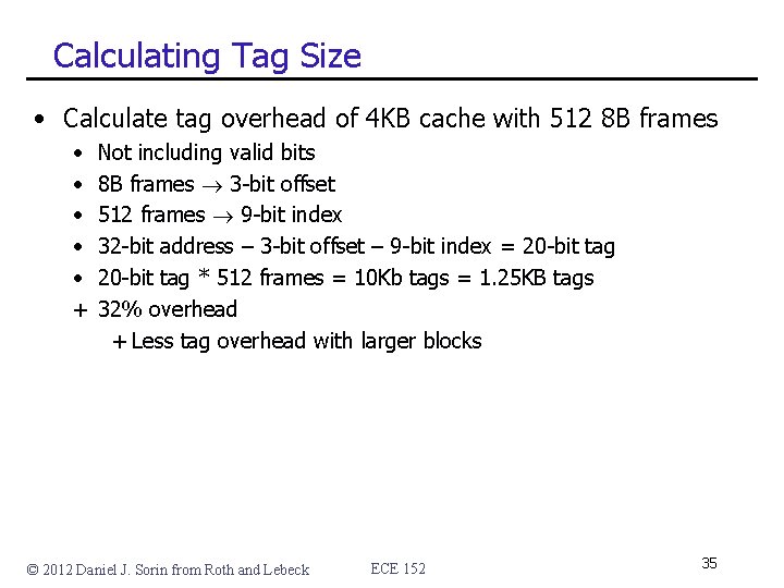
Calculating Tag Size • Calculate tag overhead of 4 KB cache with 512 8 B frames • • • + Not including valid bits 8 B frames 3 -bit offset 512 frames 9 -bit index 32 -bit address – 3 -bit offset – 9 -bit index = 20 -bit tag * 512 frames = 10 Kb tags = 1. 25 KB tags 32% overhead + Less tag overhead with larger blocks © 2012 Daniel J. Sorin from Roth and Lebeck ECE 152 35

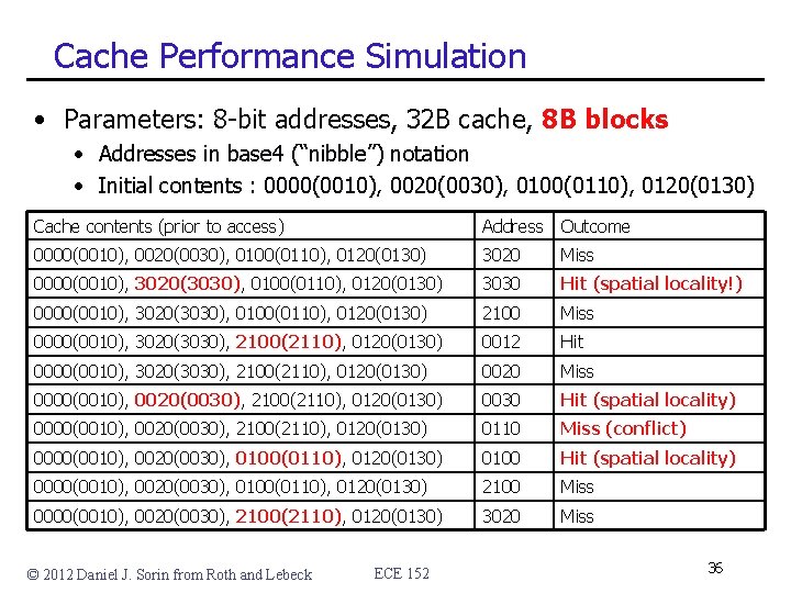
Cache Performance Simulation • Parameters: 8 -bit addresses, 32 B cache, 8 B blocks • Addresses in base 4 (“nibble”) notation • Initial contents : 0000(0010), 0020(0030), 0100(0110), 0120(0130) Cache contents (prior to access) Address Outcome 0000(0010), 0020(0030), 0100(0110), 0120(0130) 3020 Miss 0000(0010), 3020(3030), 0100(0110), 0120(0130) 3030 Hit (spatial locality!) 0000(0010), 3020(3030), 0100(0110), 0120(0130) 2100 Miss 0000(0010), 3020(3030), 2100(2110), 0120(0130) 0012 Hit 0000(0010), 3020(3030), 2100(2110), 0120(0130) 0020 Miss 0000(0010), 0020(0030), 2100(2110), 0120(0130) 0030 Hit (spatial locality) 0000(0010), 0020(0030), 2100(2110), 0120(0130) 0110 Miss (conflict) 0000(0010), 0020(0030), 0100(0110), 0120(0130) 0100 Hit (spatial locality) 0000(0010), 0020(0030), 0100(0110), 0120(0130) 2100 Miss 0000(0010), 0020(0030), 2100(2110), 0120(0130) 3020 Miss © 2012 Daniel J. Sorin from Roth and Lebeck ECE 152 36

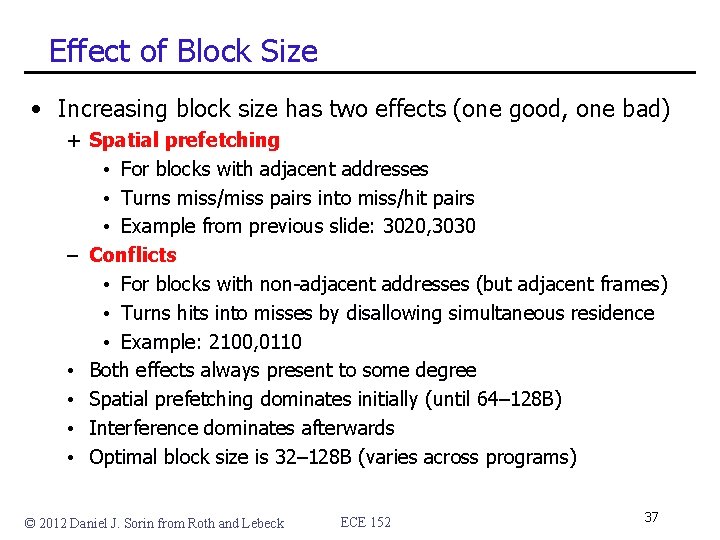
Effect of Block Size • Increasing block size has two effects (one good, one bad) + Spatial prefetching • For blocks with adjacent addresses • Turns miss/miss pairs into miss/hit pairs • Example from previous slide: 3020, 3030 – Conflicts • For blocks with non-adjacent addresses (but adjacent frames) • Turns hits into misses by disallowing simultaneous residence • Example: 2100, 0110 • Both effects always present to some degree • Spatial prefetching dominates initially (until 64– 128 B) • Interference dominates afterwards • Optimal block size is 32– 128 B (varies across programs) © 2012 Daniel J. Sorin from Roth and Lebeck ECE 152 37

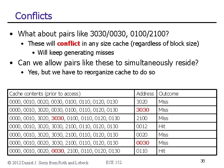
Conflicts • What about pairs like 3030/0030, 0100/2100? • These will conflict in any size cache (regardless of block size) • Will keep generating misses • Can we allow pairs like these to simultaneously reside? • Yes, but we have to reorganize cache to do so Cache contents (prior to access) Address Outcome 0000, 0010, 0020, 0030, 0100, 0110, 0120, 0130 3020 Miss 0000, 0010, 3020, 0030, 0100, 0110, 0120, 0130 3030 Miss 0000, 0010, 3020, 3030, 0100, 0110, 0120, 0130 2100 Miss 0000, 0010, 3020, 3030, 2100, 0110, 0120, 0130 0012 Hit 0000, 0010, 3020, 3030, 2100, 0110, 0120, 0130 0020 Miss 0000, 0010, 0020, 3030, 2100, 0110, 0120, 0130 0030 Miss 0000, 0010, 0020, 0030, 2100, 0110, 0120, 0130 0110 Hit © 2012 Daniel J. Sorin from Roth and Lebeck ECE 152 38

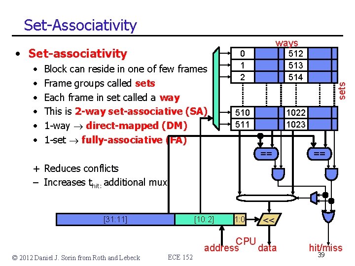
Set-Associativity • Set-associativity • • • Block can reside in one of few frames Frame groups called sets Each frame in set called a way This is 2 -way set-associative (SA) 1 -way direct-mapped (DM) 1 -set fully-associative (FA) 0 1 2 513 514 510 511 1022 1023 == sets ways == + Reduces conflicts – Increases thit: additional mux [31: 11] © 2012 Daniel J. Sorin from Roth and Lebeck [10: 2] ECE 152 1: 0 << CPU address data hit/miss 39

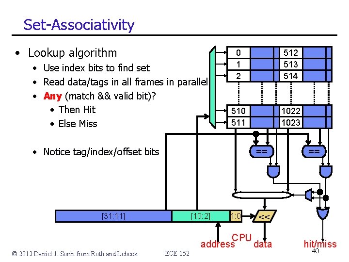
Set-Associativity • Lookup algorithm • Use index bits to find set • Read data/tags in all frames in parallel • Any (match && valid bit)? • Then Hit • Else Miss 0 1 2 513 514 510 511 1022 1023 • Notice tag/index/offset bits == [31: 11] © 2012 Daniel J. Sorin from Roth and Lebeck [10: 2] ECE 152 1: 0 == << CPU address data hit/miss 40

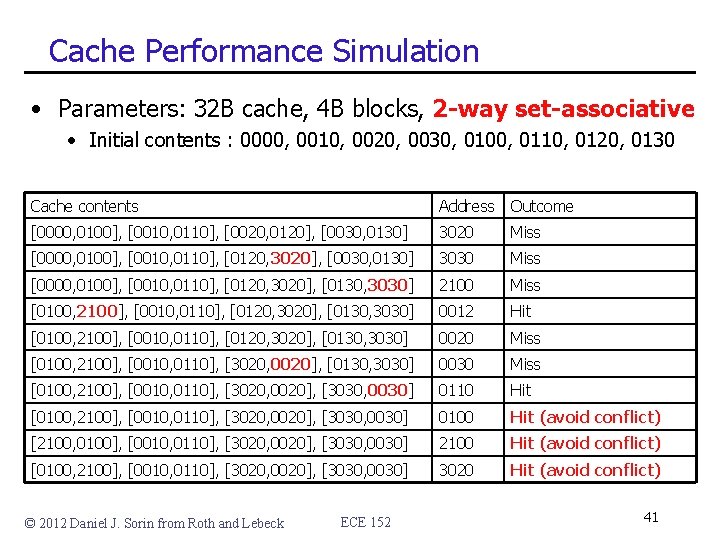
Cache Performance Simulation • Parameters: 32 B cache, 4 B blocks, 2 -way set-associative • Initial contents : 0000, 0010, 0020, 0030, 0100, 0110, 0120, 0130 Cache contents Address Outcome [0000, 0100], [0010, 0110], [0020, 0120], [0030, 0130] 3020 Miss [0000, 0100], [0010, 0110], [0120, 3020], [0030, 0130] 3030 Miss [0000, 0100], [0010, 0110], [0120, 3020], [0130, 3030] 2100 Miss [0100, 2100], [0010, 0110], [0120, 3020], [0130, 3030] 0012 Hit [0100, 2100], [0010, 0110], [0120, 3020], [0130, 3030] 0020 Miss [0100, 2100], [0010, 0110], [3020, 0020], [0130, 3030] 0030 Miss [0100, 2100], [0010, 0110], [3020, 0020], [3030, 0030] 0110 Hit [0100, 2100], [0010, 0110], [3020, 0020], [3030, 0030] 0100 Hit (avoid conflict) [2100, 0100], [0010, 0110], [3020, 0020], [3030, 0030] 2100 Hit (avoid conflict) [0100, 2100], [0010, 0110], [3020, 0020], [3030, 0030] 3020 Hit (avoid conflict) © 2012 Daniel J. Sorin from Roth and Lebeck ECE 152 41

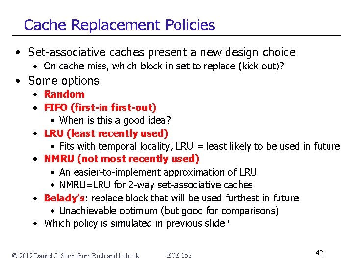
Cache Replacement Policies • Set-associative caches present a new design choice • On cache miss, which block in set to replace (kick out)? • Some options • Random • FIFO (first-in first-out) • When is this a good idea? • LRU (least recently used) • Fits with temporal locality, LRU = least likely to be used in future • NMRU (not most recently used) • An easier-to-implement approximation of LRU • NMRU=LRU for 2 -way set-associative caches • Belady’s: replace block that will be used furthest in future • Unachievable optimum (but good for comparisons) • Which policy is simulated in previous slide? © 2012 Daniel J. Sorin from Roth and Lebeck ECE 152 42

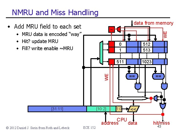
NMRU and Miss Handling data from memory • Add MRU field to each set 0 1 512 513 511 1023 WE • MRU data is encoded “way” • Hit? update MRU • Fill? write enable ~MRU WE ~ [31: 11] © 2012 Daniel J. Sorin from Roth and Lebeck [10: 2] ECE 152 == 1: 0 == << CPU address data hit/miss 43

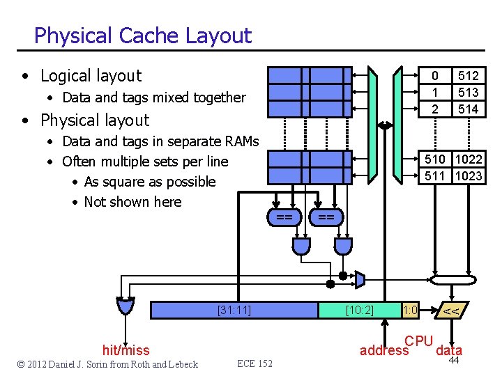
Physical Cache Layout • Logical layout 0 1 2 • Data and tags mixed together • Physical layout • Data and tags in separate RAMs • Often multiple sets per line • As square as possible • Not shown here 510 1022 511 1023 == [31: 11] hit/miss © 2012 Daniel J. Sorin from Roth and Lebeck ECE 152 513 514 == [10: 2] 1: 0 << CPU address data 44
![FullAssociativity 0 1 1022 31 2 1023 1 0 Full-Associativity 0 1 == 1022 == [31: 2] 1023 == 1: 0 == <<](https://slidetodoc.com/presentation_image_h2/bf27db5bf64566f7c1e8645616ea5c93/image-45.jpg)
Full-Associativity 0 1 == 1022 == [31: 2] 1023 == 1: 0 == << CPU • How to implement full (or at least high) associativity? • Doing it this way is terribly inefficient • 1 K matches are unavoidable, but 1 K data reads + 1 K-to-1 mux? © 2012 Daniel J. Sorin from Roth and Lebeck ECE 152 45

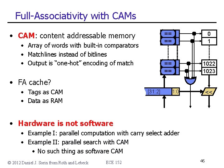
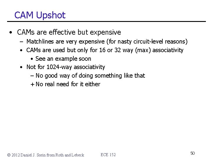
Full-Associativity with CAMs • CAM: content addressable memory • Array of words with built-in comparators • Matchlines instead of bitlines • Output is “one-hot” encoding of match == == 0 1 == == 1022 1023 • FA cache? • Tags as CAM • Data as RAM [31: 2] 1: 0 << • Hardware is not software • Example I: parallel computation with carry select adder • Example II: parallel search with CAM • No such thing as software CAM © 2012 Daniel J. Sorin from Roth and Lebeck ECE 152 46

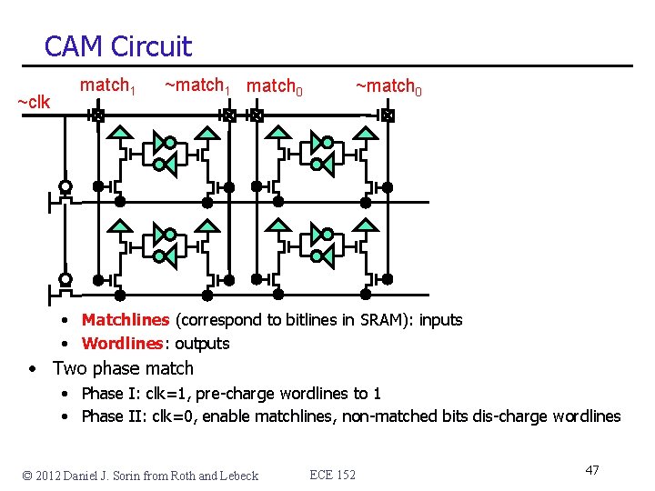
CAM Circuit ~clk match 1 ~match 1 match 0 ~match 0 • Matchlines (correspond to bitlines in SRAM): inputs • Wordlines: outputs • Two phase match • Phase I: clk=1, pre-charge wordlines to 1 • Phase II: clk=0, enable matchlines, non-matched bits dis-charge wordlines © 2012 Daniel J. Sorin from Roth and Lebeck ECE 152 47

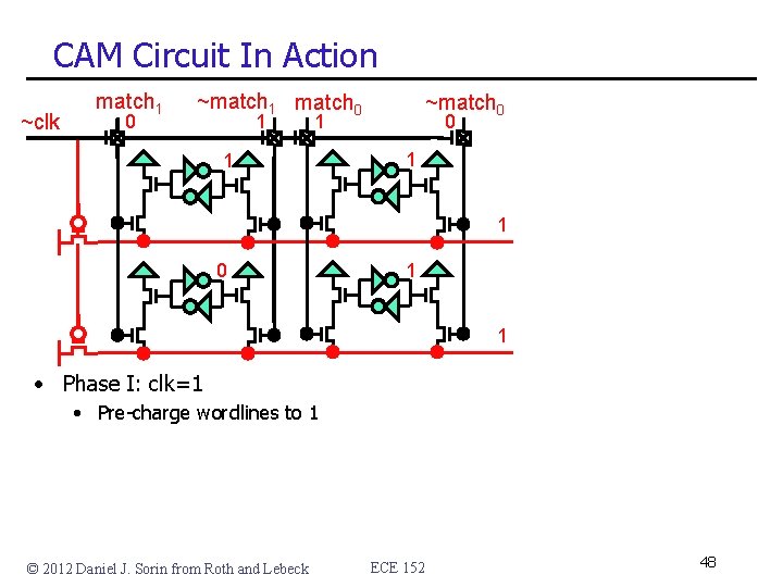
CAM Circuit In Action ~clk match 1 0 ~match 1 match 0 1 ~match 0 1 1 • Phase I: clk=1 • Pre-charge wordlines to 1 © 2012 Daniel J. Sorin from Roth and Lebeck ECE 152 48

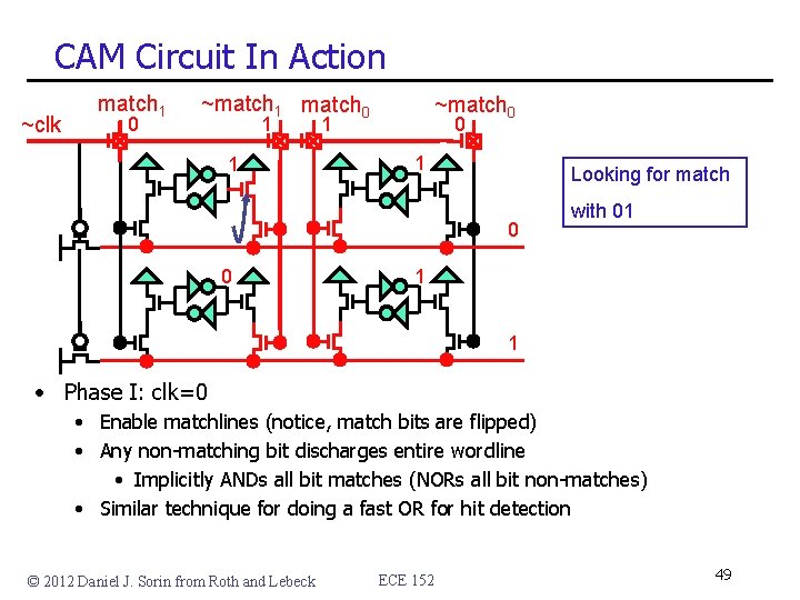
CAM Circuit In Action ~clk match 1 0 ~match 1 match 0 1 1 ~match 0 1 Looking for match 0 0 with 01 1 1 • Phase I: clk=0 • Enable matchlines (notice, match bits are flipped) • Any non-matching bit discharges entire wordline • Implicitly ANDs all bit matches (NORs all bit non-matches) • Similar technique for doing a fast OR for hit detection © 2012 Daniel J. Sorin from Roth and Lebeck ECE 152 49

CAM Upshot • CAMs are effective but expensive – Matchlines are very expensive (for nasty circuit-level reasons) • CAMs are used but only for 16 or 32 way (max) associativity • See an example soon • Not for 1024 -way associativity – No good way of doing something like that + No real need for it either © 2012 Daniel J. Sorin from Roth and Lebeck ECE 152 50

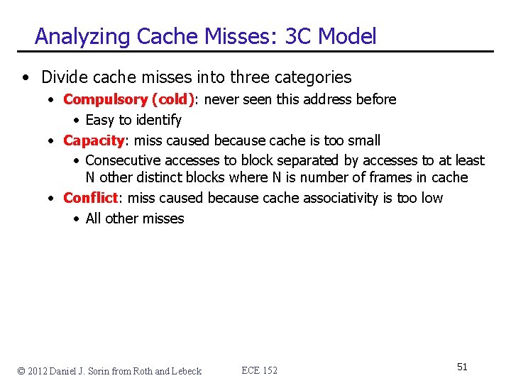
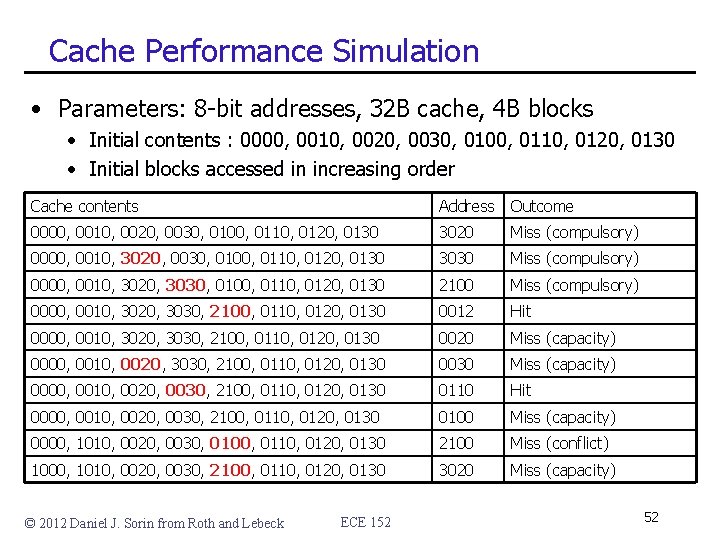
Analyzing Cache Misses: 3 C Model • Divide cache misses into three categories • Compulsory (cold): never seen this address before • Easy to identify • Capacity: miss caused because cache is too small • Consecutive accesses to block separated by accesses to at least N other distinct blocks where N is number of frames in cache • Conflict: miss caused because cache associativity is too low • All other misses © 2012 Daniel J. Sorin from Roth and Lebeck ECE 152 51

Cache Performance Simulation • Parameters: 8 -bit addresses, 32 B cache, 4 B blocks • Initial contents : 0000, 0010, 0020, 0030, 0100, 0110, 0120, 0130 • Initial blocks accessed in increasing order Cache contents Address Outcome 0000, 0010, 0020, 0030, 0100, 0110, 0120, 0130 3020 Miss (compulsory) 0000, 0010, 3020, 0030, 0100, 0110, 0120, 0130 3030 Miss (compulsory) 0000, 0010, 3020, 3030, 0100, 0110, 0120, 0130 2100 Miss (compulsory) 0000, 0010, 3020, 3030, 2100, 0110, 0120, 0130 0012 Hit 0000, 0010, 3020, 3030, 2100, 0110, 0120, 0130 0020 Miss (capacity) 0000, 0010, 0020, 3030, 2100, 0110, 0120, 0130 0030 Miss (capacity) 0000, 0010, 0020, 0030, 2100, 0110, 0120, 0130 0110 Hit 0000, 0010, 0020, 0030, 2100, 0110, 0120, 0130 0100 Miss (capacity) 0000, 1010, 0020, 0030, 0100, 0110, 0120, 0130 2100 Miss (conflict) 1000, 1010, 0020, 0030, 2100, 0110, 0120, 0130 3020 Miss (capacity) © 2012 Daniel J. Sorin from Roth and Lebeck ECE 152 52

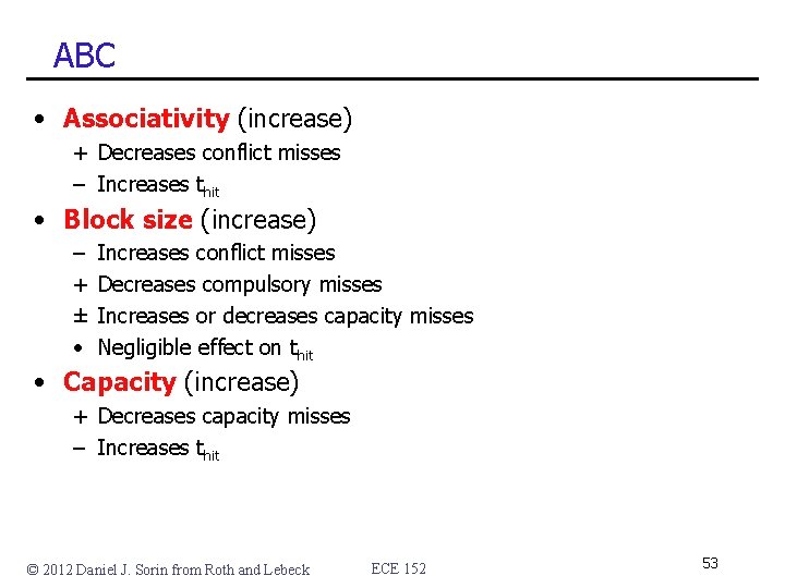
ABC • Associativity (increase) + Decreases conflict misses – Increases thit • Block size (increase) – + ± • Increases conflict misses Decreases compulsory misses Increases or decreases capacity misses Negligible effect on thit • Capacity (increase) + Decreases capacity misses – Increases thit © 2012 Daniel J. Sorin from Roth and Lebeck ECE 152 53

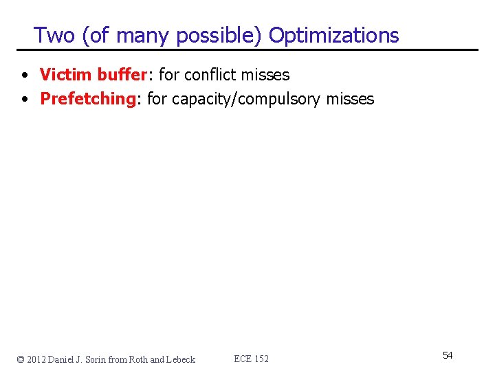
Two (of many possible) Optimizations • Victim buffer: for conflict misses • Prefetching: for capacity/compulsory misses © 2012 Daniel J. Sorin from Roth and Lebeck ECE 152 54

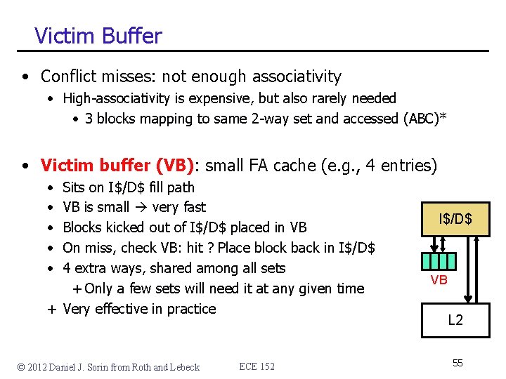
Victim Buffer • Conflict misses: not enough associativity • High-associativity is expensive, but also rarely needed • 3 blocks mapping to same 2 -way set and accessed (ABC)* • Victim buffer (VB): small FA cache (e. g. , 4 entries) • • • Sits on I$/D$ fill path VB is small very fast Blocks kicked out of I$/D$ placed in VB On miss, check VB: hit ? Place block back in I$/D$ 4 extra ways, shared among all sets + Only a few sets will need it at any given time + Very effective in practice © 2012 Daniel J. Sorin from Roth and Lebeck ECE 152 I$/D$ VB L 2 55

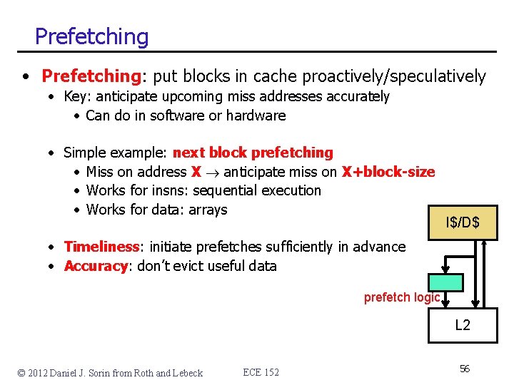
Prefetching • Prefetching: put blocks in cache proactively/speculatively • Key: anticipate upcoming miss addresses accurately • Can do in software or hardware • Simple example: next block prefetching • Miss on address X anticipate miss on X+block-size • Works for insns: sequential execution • Works for data: arrays I$/D$ • Timeliness: initiate prefetches sufficiently in advance • Accuracy: don’t evict useful data prefetch logic L 2 © 2012 Daniel J. Sorin from Roth and Lebeck ECE 152 56

Write Issues • So far we have looked at reading from cache (loads) • What about writing into cache (stores)? • Several new issues • Tag/data access • Write-through vs. write-back • Write-allocate vs. write-not-allocate © 2012 Daniel J. Sorin from Roth and Lebeck ECE 152 57

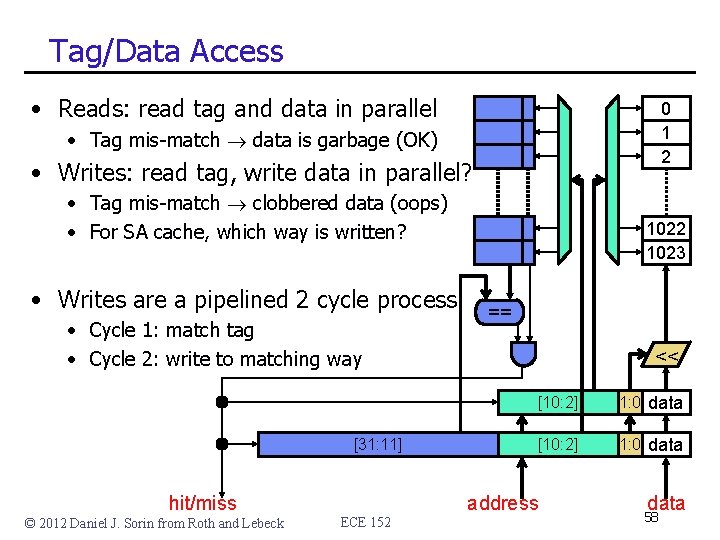
Tag/Data Access • Reads: read tag and data in parallel 0 1 2 • Tag mis-match data is garbage (OK) • Writes: read tag, write data in parallel? • Tag mis-match clobbered data (oops) • For SA cache, which way is written? • Writes are a pipelined 2 cycle process • Cycle 1: match tag • Cycle 2: write to matching way [31: 11] hit/miss © 2012 Daniel J. Sorin from Roth and Lebeck ECE 152 1023 == << [10: 2] 1: 0 data address data 58

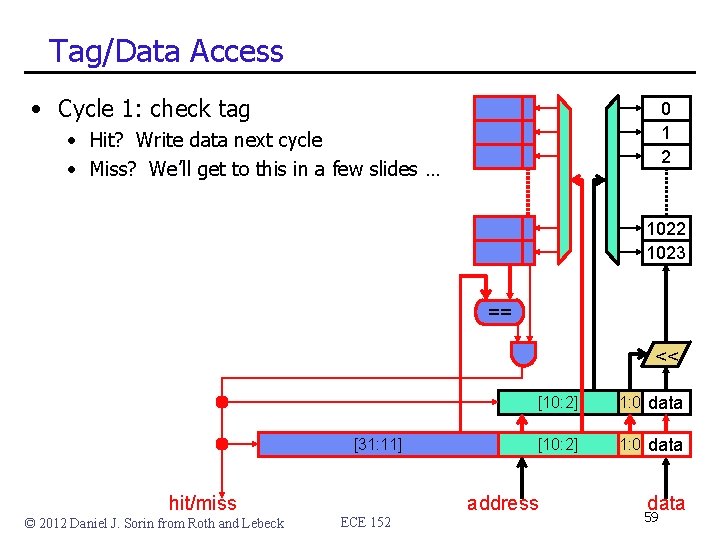
Tag/Data Access • Cycle 1: check tag 0 1 2 • Hit? Write data next cycle • Miss? We’ll get to this in a few slides … 1022 1023 == << [31: 11] hit/miss © 2012 Daniel J. Sorin from Roth and Lebeck ECE 152 [10: 2] 1: 0 data address data 59

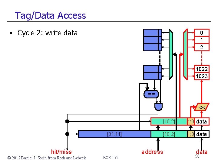
Tag/Data Access • Cycle 2: write data 0 1 2 1023 == << [31: 11] hit/miss © 2012 Daniel J. Sorin from Roth and Lebeck ECE 152 [10: 2] 1: 0 data address data 60

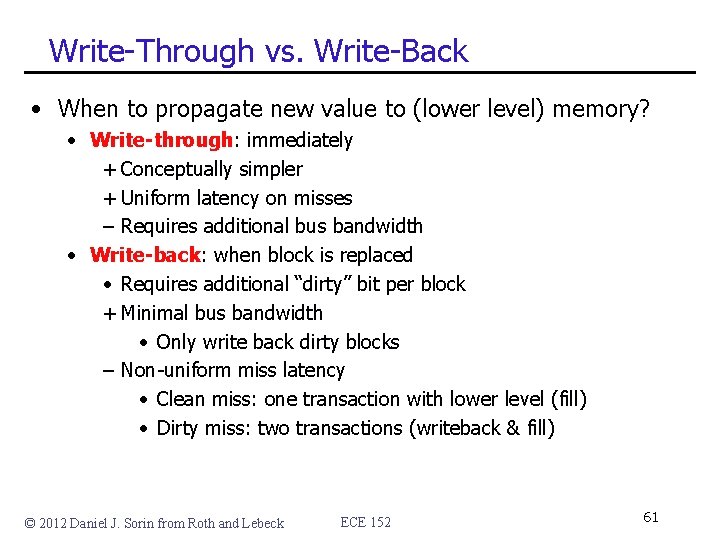
Write-Through vs. Write-Back • When to propagate new value to (lower level) memory? • Write-through: immediately + Conceptually simpler + Uniform latency on misses – Requires additional bus bandwidth • Write-back: when block is replaced • Requires additional “dirty” bit per block + Minimal bus bandwidth • Only write back dirty blocks – Non-uniform miss latency • Clean miss: one transaction with lower level (fill) • Dirty miss: two transactions (writeback & fill) © 2012 Daniel J. Sorin from Roth and Lebeck ECE 152 61

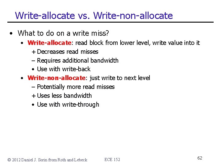
Write-allocate vs. Write-non-allocate • What to do on a write miss? • Write-allocate: read block from lower level, write value into it + Decreases read misses – Requires additional bandwidth • Use with write-back • Write-non-allocate: just write to next level – Potentially more read misses + Uses less bandwidth • Use with write-through © 2012 Daniel J. Sorin from Roth and Lebeck ECE 152 62

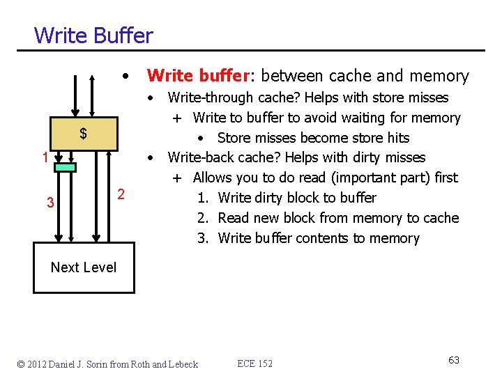
Write Buffer • Write buffer: between cache and memory • $ • 1 3 2 Write-through cache? Helps with store misses + Write to buffer to avoid waiting for memory • Store misses become store hits Write-back cache? Helps with dirty misses + Allows you to do read (important part) first 1. Write dirty block to buffer 2. Read new block from memory to cache 3. Write buffer contents to memory Next Level © 2012 Daniel J. Sorin from Roth and Lebeck ECE 152 63

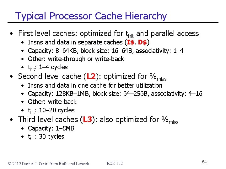
Typical Processor Cache Hierarchy • First level caches: optimized for thit and parallel access • • Insns and data in separate caches (I$, D$) Capacity: 8– 64 KB, block size: 16– 64 B, associativity: 1– 4 Other: write-through or write-back thit: 1– 4 cycles • Second level cache (L 2): optimized for %miss • • Insns and data in one cache for better utilization Capacity: 128 KB– 1 MB, block size: 64– 256 B, associativity: 4– 16 Other: write-back thit: 10– 20 cycles • Third level caches (L 3): also optimized for %miss • Capacity: 1– 8 MB • thit: 30 cycles © 2012 Daniel J. Sorin from Roth and Lebeck ECE 152 64

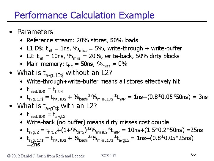
Performance Calculation Example • Parameters • • Reference stream: 20% stores, 80% loads L 1 D$: thit = 1 ns, %miss = 5%, write-through + write-buffer L 2: thit = 10 ns, %miss = 20%, write-back, 50% dirty blocks Main memory: thit = 50 ns, %miss = 0% • What is tavg. L 1 D$ without an L 2? • Write-through+write-buffer means all stores effectively hit • tmiss. L 1 D$ = thit. M • tavg. L 1 D$ = thit. L 1 D$ + %loads*%miss. L 1 D$*thit. M = 1 ns+(0. 8*0. 05*50 ns) = 3 ns • What is tavg. D$ with an L 2? • • tmiss. L 1 D$ = tavg. L 2 Write-back (no buffer) means dirty misses cost double tavg. L 2 = thit. L 2+(1+%dirty)*%miss. L 2*thit. M = 10 ns+(1. 5*0. 2*50 ns) =25 ns tavg. L 1 D$ = thit. L 1 D$ + %loads*%miss. L 1 D$*tavg. L 2 = 1 ns+(0. 8*0. 05*25 ns) =2 ns © 2012 Daniel J. Sorin from Roth and Lebeck ECE 152 65

Summary • Average access time of a memory component • tavg = thit + %miss * tmiss • Hard to get low thit and %miss in one structure hierarchy • Memory hierarchy • Cache (SRAM) memory (DRAM) swap (Disk) • Smaller, faster, more expensive bigger, slower, cheaper • SRAM • Analog technology for implementing big storage arrays • Cross-coupled inverters + bitlines + wordlines • Delay ~ √#bits * #ports © 2012 Daniel J. Sorin from Roth and Lebeck ECE 152 66

Summary, cont’d • Cache ABCs • Capacity, associativity, block size • 3 C miss model: compulsory, capacity, conflict • Some optimizations • Victim buffer for conflict misses • Prefetching for capacity, compulsory misses • Write issues • Pipelined tag/data access • Write-back vs. write-through/write-allocate vs. write-no-allocate • Write buffer Next Course Unit: Main Memory © 2012 Daniel J. Sorin from Roth and Lebeck ECE 152 67