EC 6009 ADVANCED COMPUTER ARCHITECTURE UNIT III DATA


 Single vector instruction specifies lots of work – equivalent")
 • Vector operations: arithmetic (add, sub, mul, div), memory")


 Instr. SUBV. D SUBSV. D SUBVS. D DIVV. D DIVSV.")


 for all")


 Ø Recently, multiple processors or cpu-cores have")


- Slides: 30
EC 6009 ADVANCED COMPUTER ARCHITECTURE UNIT III DATA - LEVEL PARALLELISM Vector Architecture- SIMD extensions – Graphic Processing Units – Loop Level Parallelism.
Vector Processing Definitions • Vector - a set of scalar data items, all of the same type, stored in memory. • Vector processor - an collection of hardware resources, including vector registers, functional pipelines, processing elements and register counters for performing vector operations. • Vector processing occurs when arithmetic or logical operations are applied to vectors. SCALAR (1 operation) add r 3, r 1, r 2 2 r 1 + r 3 VECTOR (N operations) v 1 v 2 + ++++ add. vv v 3, v 1, v 2 v 3 vector length
Properties of Vector Processors 1) Single vector instruction specifies lots of work – equivalent to executing an entire loop. – fewer instructions to fetch and decode. 2) Computation of each result in the vector is independent of the computation of other results in the same vector. – deep pipeline without data hazards; high clock rate 3) Hw checks for data hazards only between vector instructions (once per vector, not per vector element) 4) Access memory with known pattern – elements are all adjacent in memory => highly interleaved memory banks provides high bandwidth – access is initiated for entire vector => high memory latency is amortised (no data caches are needed) 5) Control hazards from the loop branches are reduced – nonexistent for one vector instruction 3
Properties of Vector Processors (cont’d) • Vector operations: arithmetic (add, sub, mul, div), memory accesses, effective address calculations • Multiple vector instructions can be in progress at the same time => more parallelism • Applications to benefit – Large scientific and engineering applications (car crash simulations, weather forecasting, …) – Multimedia applications 4
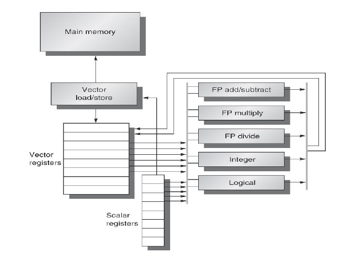
VECTOR ARCHITECTURE • • • Vector Architectures grab sets of data elements scattered about Memory, place them into large register files, operate on data in those register files and then disperse the results back into Memory. A single instruction operates on vectors of data, which results in dozens of register operations on independent data elements. These large register files acts as compiler controlled buffers, both to hide memory latency and to leverage memory bandwidth. VMIPS: Scalar portion is MIPS and its vector portion is the logical vector extension of MIPS. The primary components of the instruction set architecture of VMIPS are Vector registers Vector functional units Vector load/store unit Set of scalar registers
VECTOR ARCHITECTURE Vector registers: VMIPS has eight vector registers and each vector register hold 64 elements and 64 -bits wide. The read and write ports which total at least 16 read ports and 8 write ports are connected to the function unit inputs and outputs by a pair of crossbar Switches. Vector functional units: Each unit is fully pipelined and it can start a new operation on every clock Cycle. A control unit is needed to detect hazards. Both structural hazards for functional units and data hazards on register access. VMIPS has five functional units. For, simplicity, it is exclusively focused on the floatingpoint functional units. Vector load/store unit: The vector memory unit loads or stores a vector to or from memory. The VMIPS vector loads and stores are fully pipelined, so that words can be moved between the vector registers and memory with a bandwidth of one word per Clock cycle after an initial latency. This unit also handle scalar loads and stores. A set of Scalar registers: Scalar registers can also provide data as input to the vector functional units as well as compute addresses to pass to the vector load/store unit.
VMIPS Vector Instructions Instr. ADDVV. D ADDVS. D MULVV. D MULVS. D LV LVWS Operands Operation Comment V 1, V 2, V 3 V 1=V 2+V 3 vector + vector V 1, F 0, V 2 V 1=F 0+V 2 scalar + vector V 1, V 2, V 3 V 1=V 2 x. V 3 vector x vector V 1, F 0, V 2 V 1=F 0 x. V 2 scalar x vector V 1, R 1 V 1=M[R 1. . R 1+63] load, stride=1 V 1, R 2 V 1=M[R 1. . R 1+63*R 2] load, stride=R 2 (R 1 + i x R 2) LVI V 1, R 1, V 2 V 1=M[R 1+V 2(i), i=0. . 63] indir. ("gather") MTC 1 VLR, R 1 Vec. Len. Reg. = R 1 set vector length (Move contents of R 1 to vector-length register VL) MFC 1 R 1, VLR R 1 = Vec. Mask set vector mask (Move the contents of Vector-length register VL to R 1) 8
VMIPS Vector Instructions (cont’d) Instr. SUBV. D SUBSV. D SUBVS. D DIVV. D DIVSV. D DIVVS. D. . POP CVM Operands V 1, V 2, V 3 V 1, F 0, V 2 V 1, V 2, F 0 Operation V 1=V 2 -V 3 V 1=F 0 -V 2 V 1=V 2 - F 0 V 1=V 2/V 3 V 1=F 0/V 2 V 1=V 2/F 0 Comment vector - vector scalar – vector - scalar vector / vector scalar / vector / scalar R 1, VM Count the 1 s in the Vector Mask register Set the vector-mask register to all 1 s
VECTOR ARCHITECTURE Vectors naturally accommodate varying data sizes. One view of vector register size is 64, 64 -bit data elements, 128, 32 -bit elements, 256, 16 -bit elements and even 512, 8 -bit elements are equally valid views. Due to this hardware multiplicity, vector architecture can be useful for multimedia applications as well as scientific applications. How Vector processors work: An example Let’s take a typical problem Y=ax. X+Y X and Y are vectors initially resident in memory and a is a scalar. This problem is so called SAXPY or DAXPY loops that forms the inner loop of the Linpack Benchmark. (SAXPY stands for Single Precision a x X plus Y) (DAXPY stands for Double Precision a x X plus Y) Linpack is a collection of linear algebra routines and the Linpack benchmark Consists of routines for performing Gaussian elimination.
DAXPY: Double a X + Y Assuming vectors X, Y are length 64 L. D F 0, a ; load scalar a LV V 1, Rx ; load vector X Scalar vs. Vector MULVS V 2, V 1, F 0 ; vector-scalar mult. LV ; load vector Y V 3, Ry ADDV. D V 4, V 2, V 3 ; add L. D F 0, a SV DADDIU R 4, Rx, #512 ; last address to load loop: L. D F 2, 0(Rx) ; load X(i) MULT. D F 2, F 0, F 2 ; a*X(i) L. D F 4, 0(Ry) ; load Y(i) ADD. D F 4, F 2, F 4 ; a*X(i) + Y(i) S. D F 4, 0(Ry) ; store into Y(i) DADDIU Rx, #8 ; increment index to X DADDIU Ry, #8 ; increment index to Y DSUBU R 20, R 4, Rx ; compute bound BNEZ R 20, loop ; check if done 11 V 4, Ry ; store the result Operations: 578 (2+9*64) vs. 321 (1+5*64) (1. 8 X) Instructions: 578 (2+9*64) vs. 6 instructions (96 X) Hazards: 64 X fewer pipeline hazards
Vector Execution Time The Vector processor greatly reduces the dynamic instruction bandwidth, executing only 6 instructions versus almost 600 for MIPS. When the compiler produces vector instructions for a sequence and the resulting code spends much of its time running in a vector mode, the code is said to be Vectorized or Vectorizable. Loops can be Vectorized when they do not have dependencies between iterations of a loop which are called loop carried dependences. In the MIPS code every ADD. D must wait for a MUL. D and every S. D must wait for the ADD. D. On the Vector processor each vector instruction will only stall for the first element in each vector and then subsequent elements will flow smoothly down the pipeline. 12
Vector Execution Time The execution time of a sequence of vector operations primarily depends on three factors (1) the length of the operands (2) Structural hazards among the operation (3) the data dependences. Convoy is the set of vector instructions that could potentially execute together. The instructions in a convoy must not contain any structural Hazards, if such hazards were present, the instructions would need to be Serialized and initiated in different convoys. 13
Vector Execution Time Show the following code sequence lays out in convoys, assuming a single copy of each vector functional unit: 1: LV V 1, Rx ; load vector X 2: MULVS. D V 2, V 1, F 0 ; vector-scalar multiply. LV V 3, Ry ; load vector Y 3: ADDV. D V 4, V 2, V 3 ; add 4: SV Ry, V 4 ; store the result How many chimes will this vector sequence take? How many cycles per FLOP (floating point operation) are needed, ignoring vector instruction issue overhead? The first convoy starts with the first LV instruction. The MULVS. D is dependent on the first LV, but chaining allows it to be in the same convoy. The second LV instruction must be in a separate convoy since there is a structural hazard on the load/store unit for the prior LV instruction. The ADDVV. D is dependent on the second LV, but it can be in the same convoy via chaining.
Vector Execution Time Finally, the SV has a structural hazard on the LV in the second convoy, so it must go in the third convoy. 1. LV MULVS. D 2. LV ADDVV. D 3. SV The sequence requires three convoys. Since the sequence takes three chimes and there are two floating point operations per result, the number of cycles per FLOP is 1. 5. For example for 64 -element vectors, the time in chime s is 3, so the Sequence would take about 64 X 3 =192 clock cycles. (Chime – unit of time taken to execute one convoy. )
Multiple Lanes • C=A+B • The Vector processor on the left has a single add pipeline and can complete one addition per cycle. • The Vector processor on the right has four add pipelines and can complete four additions per cycle. • The set of elements that move through the pipeline together is termed an element group. • Figure shows the structure of a four lane unit. Thus, going to four lanes from one lane reduces the number of clocks for a chime from 64 to 16. • Each lane contains one portion of the vector register file and one execution pipeline from each vector functional unit. • Each vector functional unit executes vector instructions at the rate of one element group per cycle using multiple pipelines.
Multiple Lanes • The first lane holds the first element (element 0) for all vector registers and so the first element in any Vector instruction will have its source and destination operands located in the first lane. • This allocation avoids inter-lane communication and reduces the wiring cost and register file ports required to build a highly parallel execution unit. • Due to this reason Vector computers can complete up to 64 operations per clock cycle. ( 2 arithmetic units and 2 load/store unit across 16 lanes) • Adding multiple lanes is a popular technique to improve vector performance as it requires little increase in control complexity and does not require changes to existing machine code. • It also allows designers to trade off die area, clock rate, voltage and energy without sacrificing peak performance.
Vector – Length Registers: Handling Loops Not Equal to 64 • A vector register processor has a natural vector length determined by the number of elements in each vector register. • This length, which is 64 for VMIPS is unlikely to match the real vector length in a program. • Moreover in a real program the length of a particular vector operation is often unknown at compile time. • For example consider this code for (i = 0; i < n; i=i+1) Y[i] = a* X[i] + Y[i]; The size of all the vector operations depends on n, which may not even known until runtime. • The solution to these problems is to create a vector – length register (VLR). The VLR controls the length of any vector operation, including a vector load or store. • This solves problem as long as the real length is less than or equal to the Maximum Vector Length (MVL).
Vector Mask Registers : Handling IF statement in Vector Loops • From Amdahl’s law, we know that the speedup on programs with low to moderate levels of vectorization will be very limited. • The presence of conditionals (IF statements) inside loops and the use of sparse matrices are two main reasons for lower levels of vectorization. • Program that contain IF statements in a loops cannot be run in vector mode it introduce control dependences into a loop. • For example consider this code for (i = 0; i < 64; i=i+1) if (X[i] != 0) X[i] = X[i] – Y[i]; • This loop cannot normally be vectorized because of the conditional execution of the body; however, if the inner loop could be run for the iterations for which X[i] not equal to 0, then the subtraction could be vectorized.
Vector Mask Registers : Handling IF statement in Vector Loops • We can now use the following code for the previous loop, assuming that the starting addresses of X and Y are in Rx and Ry, respectively. LV LV L. D SNEVS. D SUBVV. D SV V 1, Rx V 2, Ry F 0, #0 V 1, F 0 V 1, V 2 Rx, V 1 ; load vector X into V 1 ; load vector Y ; load FP zero into F 0 ; sets VM(i) to 1 if V 1(i)!=F 0 ; subtract under vector mask ; store the result in X • Compiler writers call the transformation to change an IF statement to a straight line code sequence using conditional execution.
Vector Mask Registers : Handling IF statement in Vector Loops • Most vector processors use memory banks, which allow multiple independent accesses rather than simple memory interleaving for three reasons. 1. To support simultaneous accesses from multiple loads or stores, the memory system needs multiple banks and be able to control the addresses to the banks independently. 2. Most vector processors support the ability to load or store data words that are not sequential. In such cases, independent bank addressing, rather than interleaving is required. 3. Most vector computers support multiple processors sharing the same memory system, so each processor will be generating its own independent stream of addresses.
Vector Mask Registers : Handling IF statement in Vector Loops • Example: The largest configuration of Cray T 90 has 32 processors, each capable of generating 4 loads and 2 stores per cycle. The processor clock cycle is 2. 167 n. S, while the cycle time of the SRAMs used in the memory system is 15 n. S. Calculate the minimum number of memory banks required to allow all processors to run at full memory bandwidth. • 32 x 6=192 accesses, • SRAM bank is busy for 15/2. 167≈7 clock cycles. • 192 X 7 = 1344 memory banks.
Stride • Example: 8 memory banks with a bank busy time of 6 cycles and a total memory latency of 12 cycles. How long will it take to complete a 64 -element vector load with a stride of 1? With a stride of 32? • Answer: – Stride of 1: number of banks is greater than the bank busy time, so it takes • 12+64 = 76 clock cycles 1. 2 cycle per element – Stride of 32: the worst case scenario happens when the stride value is a multiple of the number of banks, which this is! Every access to memory will collide with the previous one! Thus, the total time will be: • 12 + 1 + 6 * 63 = 391 clock cycles, or 6. 1 clock cycles per element!
GATHER AND SCATTER (P. No 278 -280) Ø Recently, multiple processors or cpu-cores have been widely used in high performance clusters. In the machine of such clusters, the multiple processes are running at the same time. Ø If all processes enter the I/O phase at the same time and issue the I/O requests simultaneously, the I/O node of parallel file systems has the possibility to receive I/O requests from all applications. Ø Each process tends to issue the contiguous requests, but they can be interrupted by the requests of other nodes in the case of multi process. Then, the I/O node receives these requests as non-contiguous fashion. This increases the disk seek time at the I/O node and results in the severe performance degradation. Ø A new I/O architecture for parallel file systems, called the Gather-Arrange. Scatter (GAS) architecture, is introduced in order to reduce the disk seek time and the number of I/O requests in parallel file systems on multi-core clusters. Ø In the GAS architecture, the I/O requests from the same node are gathered locally, then arranged to the better order, and finally scattered to the remote disks in parallel. To gather the requests, they are issued asynchronously from the viewpoint of the application.
SIMD EXTENSIONS The Roofline Visual performance Model: One way to compare floating - point performance of SIMD architectures is the Roofline model. It ties together memory performance and arithmetic intensity in a two dimensional graph. Arithmetic intensity is the ratio of floating point operations per byte of memory accessed. It can be calculated by taking the total number of floating point operations for a program divided by the total number of data bytes transferred to main memory during program execution. Figure shows the Roofline model for NEC SX-9 vector processor on the left and the Intel core i 7 920 multi-core computer on the right. The vertical Y-axis is achievable floating point performance from 2 to 256 GFLOP/sec. The horizontal X-axis is arithmetic intensity, varying from 1/8 th FLOP/DRAM byte accessed to 16 FLOP/DRAM byte accessed in both graphs. Note that the graph is a log-log scale.
Examples • Attainable GFLOPs/sec Min = (Peak Memory BW × Arithmetic Intensity, Peak Floating Point Perf. )
SIMD EXTENSIONS The X axis is FLOP/byte and the Y axis is FLOP/sec, bytes/sec is just a diagonal line at a 45 degree angle in the figure. One way to compare floating - point performance of SIMD architectures is the Roofline model. Attainable GFLOPs/sec = Min (Peak memory BW X Arithmetic Intensity, peak floating-point performance) If Arithmetic intensity hits the flat part of the roof, which means performance is computationally limited, or it hits the slanted part of the roof, which means performance is ultimately limited by memory BW. The peak computational performance of the SX-9 is 2. 4 times faster than core i 7, but the memory performance is 10 X faster.
SIMILARITIES AND DIFFERENCES BETWEEN SIMD COMPUTERS AND GPU’S 1. Both are multiprocessors whose processors use multiple SIMD lanes, although GPU have more processors and many more lanes. 2. Both use a 64 -bit address space, although the physical main memory is much smaller in GPU’s. 3. Both have similar performance ratios between single -precision and double precision and floating point arithmetic. 4. Both use caches. GPU use smaller streaming caches and multicore computers use large multilevel caches. 5. Unlike GPUs multimedia SIMD instructions do not support gather-scatter memory accesses.
SIMILARITIES AND DIFFERENCES BETWEEN VECTOR ARCHITECTURES AND GPU’S 1. Both architectures are designed to execute data-level parallelism. 2. A SIMD processor is like a vector processor. The multiple SIMD processors in GPUs acts as independent MIMD cores. The biggest difference is multithreading, which is fundamental to GPUs and missing from most vector processors. 3. A VIMPS processor has 8 vector registers with 64 elements or 512 elements total. A GPU thread has up to 64 registers with 32 elements or 2048 elements. These extra GPU registers support multithreading. 4. There are many more lanes in GPU’s, so GPU chimes are shorter. While a vector processor might have 2 to 8 lanes. 5. The closest GPU terms to a vectorized loop is Grid and a PTX instruction is the closest to a vector instruction. 6. Vector loads and stores are like a block transfer between memory and the Vector register. In contrast, GPU hide memory latency using multithreading. 7. The control processor of a vector computer plays an important role, it broadcasts operations to all the vector lanes and broadcast a scalar register value for vector-scalar operations. The control processor is missing in the GPU. 8. The scalar processor can be slower than a vector processor floating-point computations in a vector computer. The simple scalar processor in a vector computer is likely to be faster and more power efficient than the GPU. 9. Vector uses main memory where GPU uses GPU memory.
GRAPHIC PROCESSING UNITS • To increase hardware utilization each SIMD processor has two SIMD thread schedulers and two instruction dispatch units. • The dual SIMD thread scheduler selects two threads of SIMD instructions and issues one instruction from each to two sets of 16 SIMD lanes, 16 load/store units, or 4 special function units. • Two threads of SIMD instructions are scheduled every two clock cycles to any of these collections. Since threads are independent there is no need to check for data dependencies in the instruction stream. The multithreaded vector processor that can issue vector instructions from two independent threads. • First figure shows that the dual scheduler issuing instruction and second figure shows the block diagram of the multithreaded SIMD processor of a Fermi GPU. • Fermi introduces several innovations to bring GPU’s much closer to system processor than Tesla and previous generations of GPU architectures. • Refer P. No 292, 298 and 305 -308 (Fermi GPU Architecture)