E 85 Digital Design Computer Engineering Lecture 1
- Slides: 48

E 85 Digital Design & Computer Engineering Lecture 1: Logic Gates & Analog Behavior of Digital Systems

Lecture 1 • • • Logic Gates Verilog Logic Levels CMOS Transistors Power Consumption Datasheets Digital Design and Computer Architecture: ARM® Edition © 2015 Lecture 1 <2>

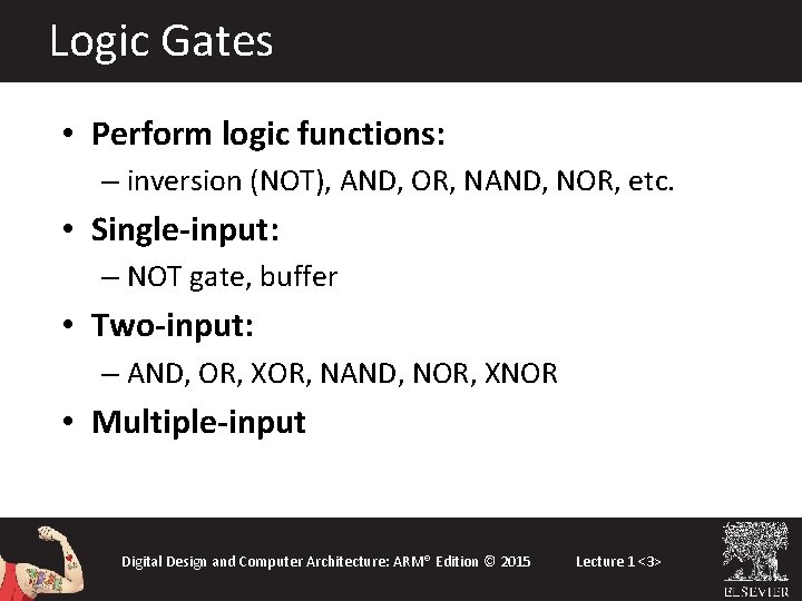
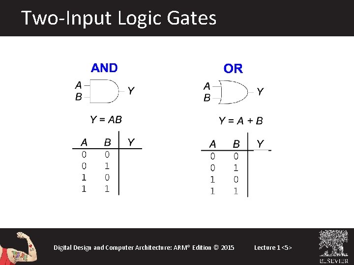
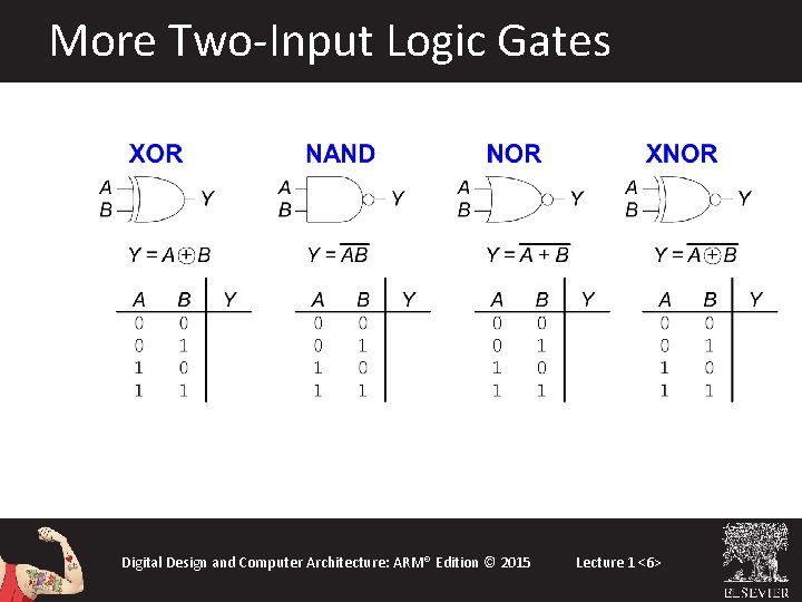
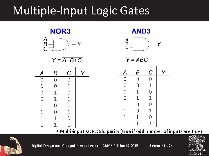
Logic Gates • Perform logic functions: – inversion (NOT), AND, OR, NAND, NOR, etc. • Single-input: – NOT gate, buffer • Two-input: – AND, OR, XOR, NAND, NOR, XNOR • Multiple-input Digital Design and Computer Architecture: ARM® Edition © 2015 Lecture 1 <3>

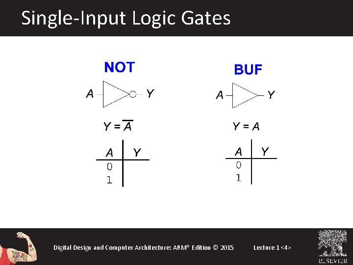
Single-Input Logic Gates Digital Design and Computer Architecture: ARM® Edition © 2015 Lecture 1 <4>

Two-Input Logic Gates Digital Design and Computer Architecture: ARM® Edition © 2015 Lecture 1 <5>

More Two-Input Logic Gates Digital Design and Computer Architecture: ARM® Edition © 2015 Lecture 1 <6>

Multiple-Input Logic Gates • Multi-input XOR: Odd parity (true if odd number of inputs are true) Digital Design and Computer Architecture: ARM® Edition © 2015 Lecture 1 <7>

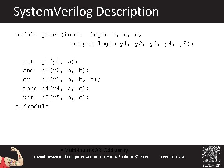
System. Verilog Description module gates(input logic a, b, c, output logic y 1, y 2, y 3, y 4, y 5); not g 1(y 1, and g 2(y 2, or g 3(y 3, nand g 4(y 4, xor g 5(y 5, endmodule a); a, b, c); a, c); • Multi-input XOR: Odd parity Digital Design and Computer Architecture: ARM® Edition © 2015 Lecture 1 <8>

Logic Levels • Discrete voltages represent 1 and 0 • For example: – 0 = ground (GND) or 0 volts – 1 = VDD or 5 volts • What about 4. 99 volts? Is that a 0 or a 1? • What about 3. 2 volts? Digital Design and Computer Architecture: ARM® Edition © 2015 Lecture 1 <9>

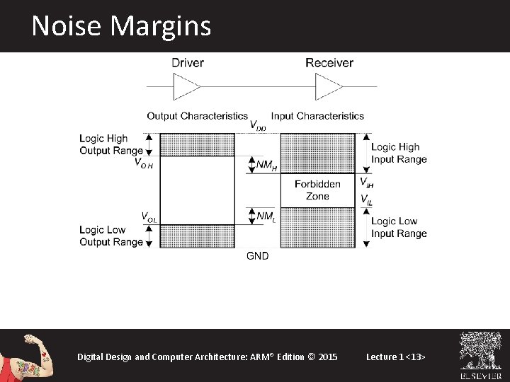
Logic Levels • Range of voltages for 1 and 0 • Different ranges for inputs and outputs to allow for noise Digital Design and Computer Architecture: ARM® Edition © 2015 Lecture 1 <10>

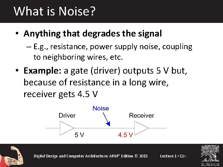
What is Noise? • Anything that degrades the signal – E. g. , resistance, power supply noise, coupling to neighboring wires, etc. • Example: a gate (driver) outputs 5 V but, because of resistance in a long wire, receiver gets 4. 5 V Digital Design and Computer Architecture: ARM® Edition © 2015 Lecture 1 <11>

The Static Discipline • With logically valid inputs, every circuit element must produce logically valid outputs • Use limited ranges of voltages to represent discrete values Digital Design and Computer Architecture: ARM® Edition © 2015 Lecture 1 <12>

Noise Margins Digital Design and Computer Architecture: ARM® Edition © 2015 Lecture 1 <13>

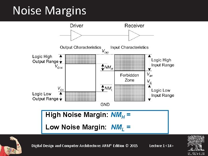
Noise Margins High Noise Margin: NMH = VOH – VIH Low Noise Margin: NML = VIL – VOL Digital Design and Computer Architecture: ARM® Edition © 2015 Lecture 1 <14>

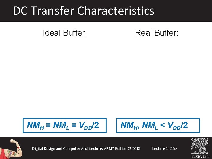
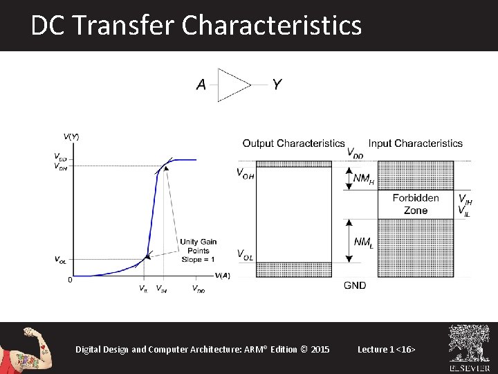
DC Transfer Characteristics Ideal Buffer: NMH = NML = VDD/2 Real Buffer: NMH, NML < VDD/2 Digital Design and Computer Architecture: ARM® Edition © 2015 Lecture 1 <15>

DC Transfer Characteristics Digital Design and Computer Architecture: ARM® Edition © 2015 Lecture 1 <16>

VDD Scaling • In 1970’s and 1980’s, VDD = 5 V • VDD has dropped – Avoid frying tiny transistors – Save power • 3. 3 V, 2. 5 V, 1. 8 V, 1. 5 V, 1. 2 V, 1. 0 V, … – Be careful connecting chips with different supply voltages Digital Design and Computer Architecture: ARM® Edition © 2015 Lecture 1 <17>

VDD Scaling • In 1970’s and 1980’s, VDD = 5 V • VDD has dropped – Avoid frying tiny transistors – Save power • 3. 3 V, 2. 5 V, 1. 8 V, 1. 5 V, 1. 2 V, 1. 0 V, … – Be careful connecting chips with different supply voltages Chips operate because they contain magic smoke Proof: if the magic smoke is let out, the chip stops working Digital Design and Computer Architecture: ARM® Edition © 2015 Lecture 1 <18>

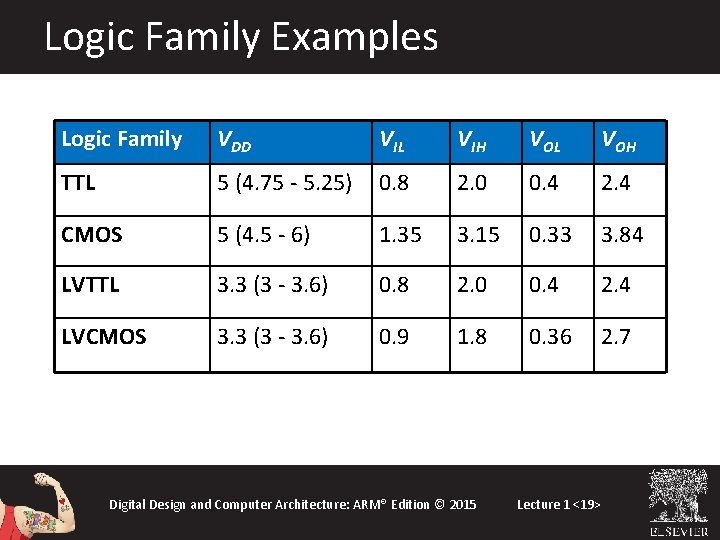
Logic Family Examples Logic Family VDD VIL VIH VOL VOH TTL 5 (4. 75 - 5. 25) 0. 8 2. 0 0. 4 2. 4 CMOS 5 (4. 5 - 6) 1. 35 3. 15 0. 33 3. 84 LVTTL 3. 3 (3 - 3. 6) 0. 8 2. 0 0. 4 2. 4 LVCMOS 3. 3 (3 - 3. 6) 0. 9 1. 8 0. 36 2. 7 Digital Design and Computer Architecture: ARM® Edition © 2015 Lecture 1 <19>

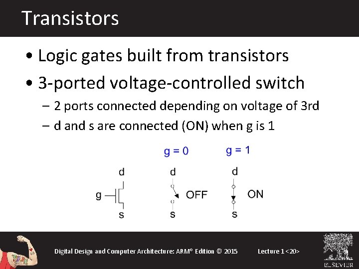
Transistors • Logic gates built from transistors • 3 -ported voltage-controlled switch – 2 ports connected depending on voltage of 3 rd – d and s are connected (ON) when g is 1 Digital Design and Computer Architecture: ARM® Edition © 2015 Lecture 1 <20>

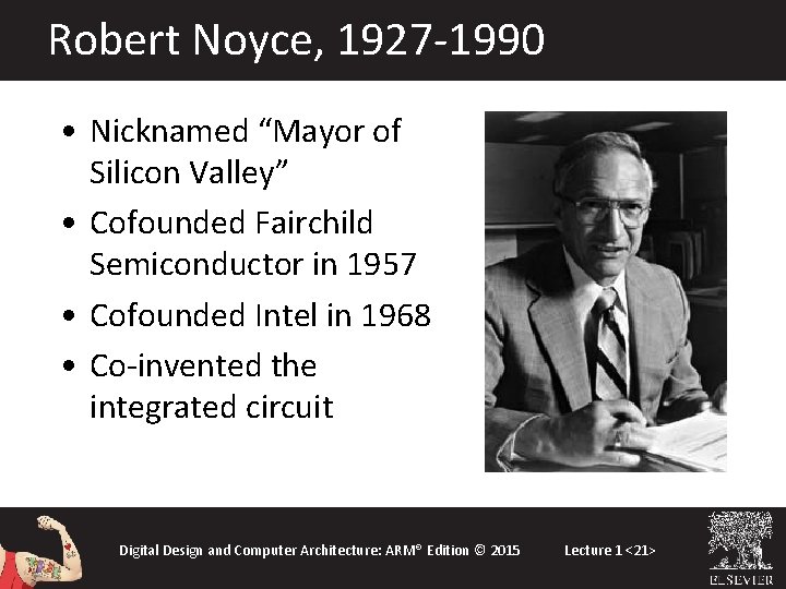
Robert Noyce, 1927 -1990 • Nicknamed “Mayor of Silicon Valley” • Cofounded Fairchild Semiconductor in 1957 • Cofounded Intel in 1968 • Co-invented the integrated circuit Digital Design and Computer Architecture: ARM® Edition © 2015 Lecture 1 <21>

Silicon • Transistors built from silicon, a semiconductor • Pure silicon is a poor conductor (no free charges) • Doped silicon is a good conductor (free charges) – n-type (free negative charges, electrons) – p-type (free positive charges, holes) Digital Design and Computer Architecture: ARM® Edition © 2015 Lecture 1 <22>

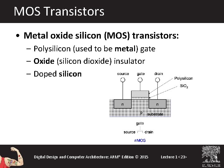
MOS Transistors • Metal oxide silicon (MOS) transistors: – Polysilicon (used to be metal) gate – Oxide (silicon dioxide) insulator – Doped silicon Digital Design and Computer Architecture: ARM® Edition © 2015 Lecture 1 <23>

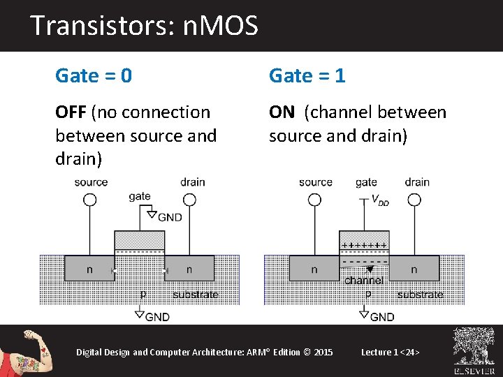
Transistors: n. MOS Gate = 0 Gate = 1 OFF (no connection between source and drain) ON (channel between source and drain) Digital Design and Computer Architecture: ARM® Edition © 2015 Lecture 1 <24>

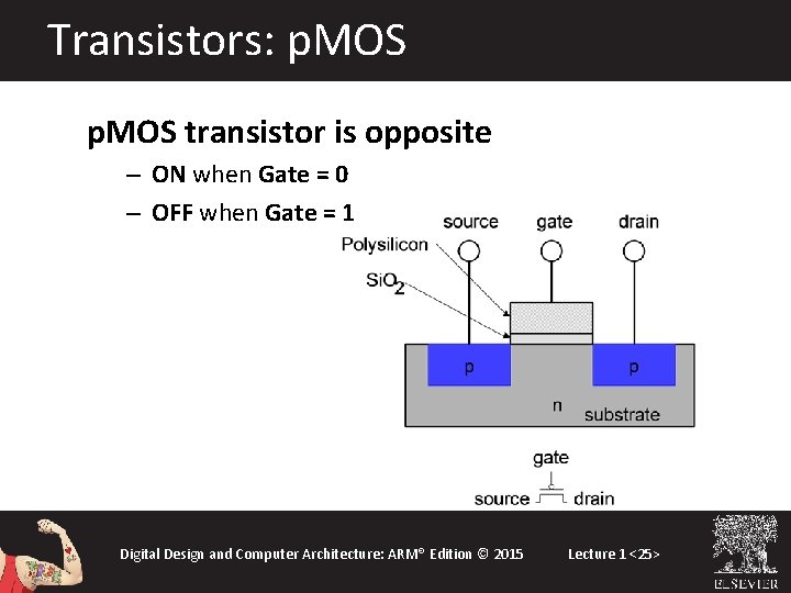
Transistors: p. MOS transistor is opposite – ON when Gate = 0 – OFF when Gate = 1 Digital Design and Computer Architecture: ARM® Edition © 2015 Lecture 1 <25>

Transistor Function Digital Design and Computer Architecture: ARM® Edition © 2015 Lecture 1 <26>

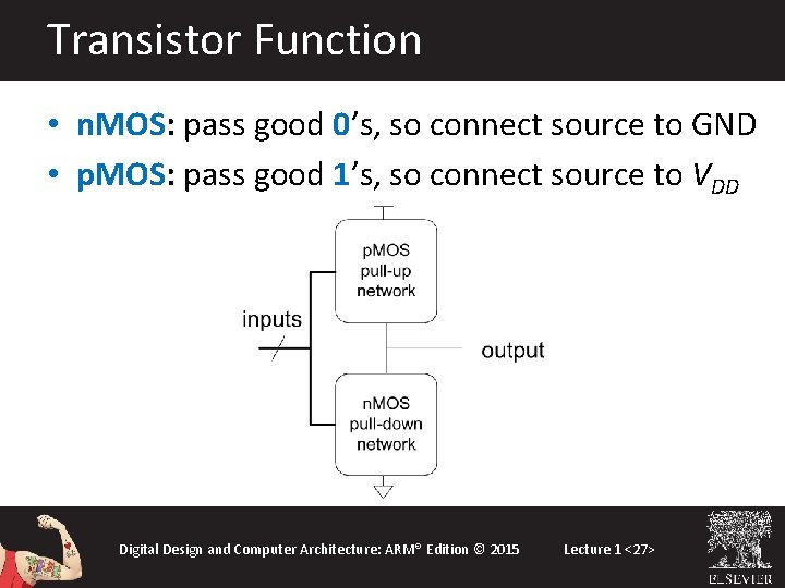
Transistor Function • n. MOS: pass good 0’s, so connect source to GND • p. MOS: pass good 1’s, so connect source to VDD Digital Design and Computer Architecture: ARM® Edition © 2015 Lecture 1 <27>

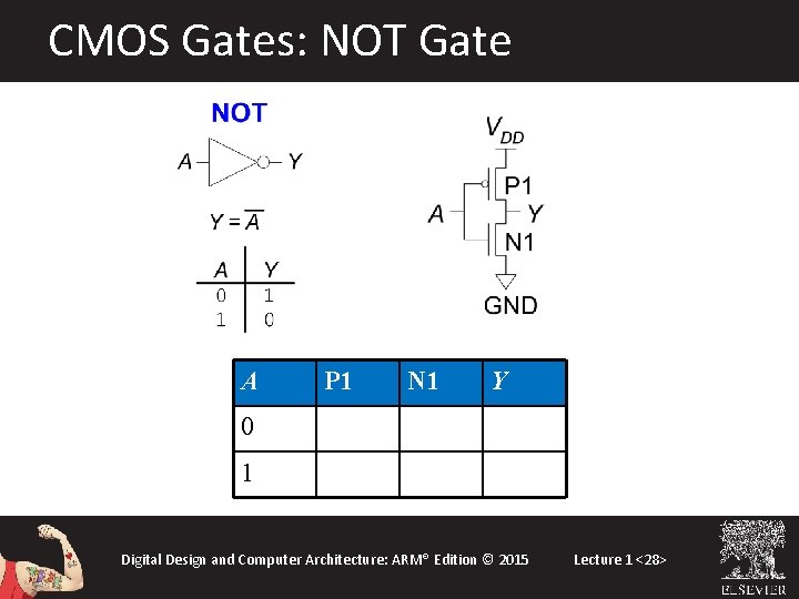
CMOS Gates: NOT Gate A P 1 N 1 Y 0 ON OFF 1 1 OFF ON 0 Digital Design and Computer Architecture: ARM® Edition © 2015 Lecture 1 <28>

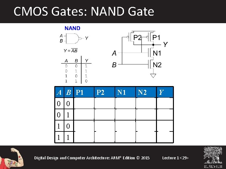
CMOS Gates: NAND Gate A 0 0 1 B 0 1 0 P 1 ON ON OFF P 2 ON OFF ON N 1 OFF ON 1 1 OFF ON N 2 OFF ON OFF Y 1 1 1 ON 0 Digital Design and Computer Architecture: ARM® Edition © 2015 Lecture 1 <29>

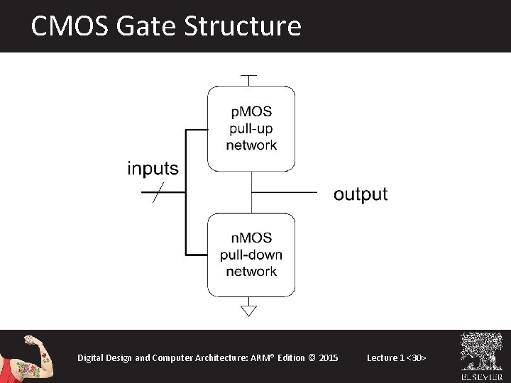
CMOS Gate Structure Digital Design and Computer Architecture: ARM® Edition © 2015 Lecture 1 <30>

NOR 3 Gate How do you build a three-input NOR gate? Digital Design and Computer Architecture: ARM® Edition © 2015 Lecture 1 <31>

AND 2 Gate How do you build a two-input AND gate? Digital Design and Computer Architecture: ARM® Edition © 2015 Lecture 1 <32>

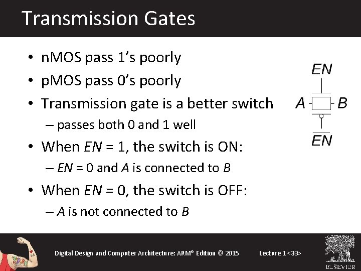
Transmission Gates • n. MOS pass 1’s poorly • p. MOS pass 0’s poorly • Transmission gate is a better switch – passes both 0 and 1 well • When EN = 1, the switch is ON: – EN = 0 and A is connected to B • When EN = 0, the switch is OFF: – A is not connected to B Digital Design and Computer Architecture: ARM® Edition © 2015 Lecture 1 <33>

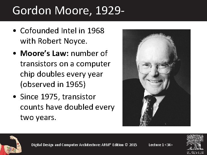
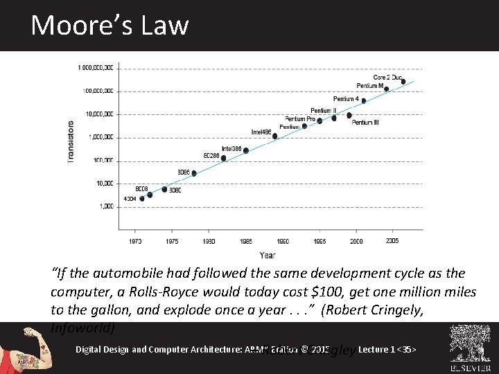
Gordon Moore, 1929 • Cofounded Intel in 1968 with Robert Noyce. • Moore’s Law: number of transistors on a computer chip doubles every year (observed in 1965) • Since 1975, transistor counts have doubled every two years. Digital Design and Computer Architecture: ARM® Edition © 2015 Lecture 1 <34>

Moore’s Law “If the automobile had followed the same development cycle as the computer, a Rolls-Royce would today cost $100, get one million miles to the gallon, and explode once a year. . . ” (Robert Cringely, Infoworld) Digital Design and Computer Architecture: ARM® Edition ©Cringley 2015 Lecture 1 <35> – Robert

Power Consumption Power = Energy consumed per unit time • Dynamic power consumption • Static power consumption Digital Design and Computer Architecture: ARM® Edition © 2015 Lecture 1 <36>

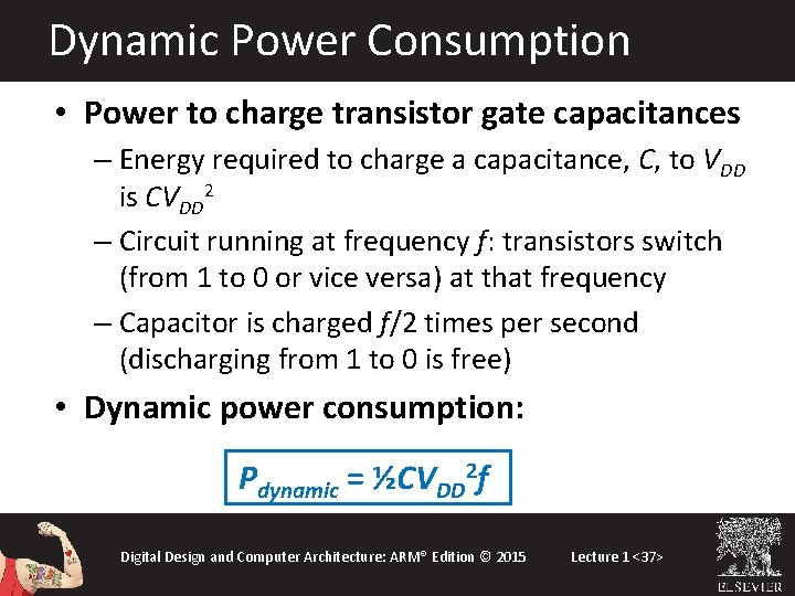
Dynamic Power Consumption • Power to charge transistor gate capacitances – Energy required to charge a capacitance, C, to VDD is CVDD 2 – Circuit running at frequency f: transistors switch (from 1 to 0 or vice versa) at that frequency – Capacitor is charged f/2 times per second (discharging from 1 to 0 is free) • Dynamic power consumption: Pdynamic = ½CVDD 2 f Digital Design and Computer Architecture: ARM® Edition © 2015 Lecture 1 <37>

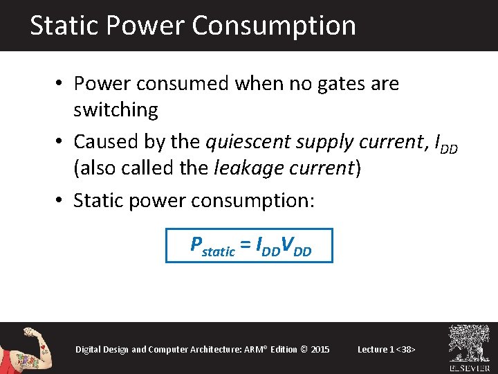
Static Power Consumption • Power consumed when no gates are switching • Caused by the quiescent supply current, IDD (also called the leakage current) • Static power consumption: Pstatic = IDDVDD Digital Design and Computer Architecture: ARM® Edition © 2015 Lecture 1 <38>

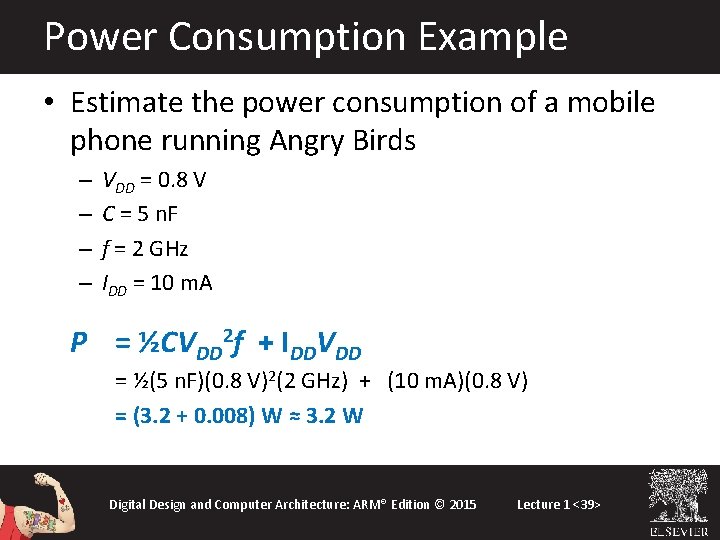
Power Consumption Example • Estimate the power consumption of a mobile phone running Angry Birds – – VDD = 0. 8 V C = 5 n. F f = 2 GHz IDD = 10 m. A P = ½CVDD 2 f + IDDVDD = ½(5 n. F)(0. 8 V)2(2 GHz) + (10 m. A)(0. 8 V) = (3. 2 + 0. 008) W ≈ 3. 2 W Digital Design and Computer Architecture: ARM® Edition © 2015 Lecture 1 <39>

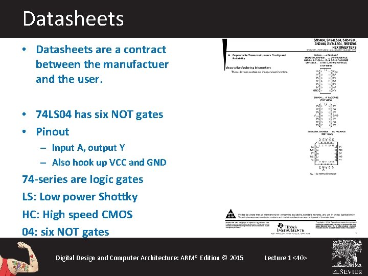
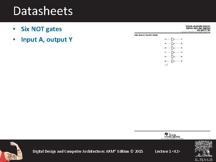
Datasheets • Datasheets are a contract between the manufactuer and the user. • 74 LS 04 has six NOT gates • Pinout – Input A, output Y – Also hook up VCC and GND 74 -series are logic gates LS: Low power Shottky HC: High speed CMOS 04: six NOT gates Digital Design and Computer Architecture: ARM® Edition © 2015 Lecture 1 <40>

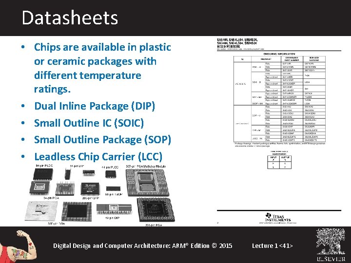
Datasheets • Chips are available in plastic or ceramic packages with different temperature ratings. • Dual Inline Package (DIP) • Small Outline IC (SOIC) • Small Outline Package (SOP) • Leadless Chip Carrier (LCC) Digital Design and Computer Architecture: ARM® Edition © 2015 Lecture 1 <41>

Datasheets • Six NOT gates • Input A, output Y Digital Design and Computer Architecture: ARM® Edition © 2015 Lecture 1 <42>

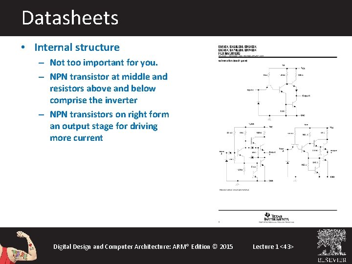
Datasheets • Internal structure – Not too important for you. – NPN transistor at middle and resistors above and below comprise the inverter – NPN transistors on right form an output stage for driving more current Digital Design and Computer Architecture: ARM® Edition © 2015 Lecture 1 <43>

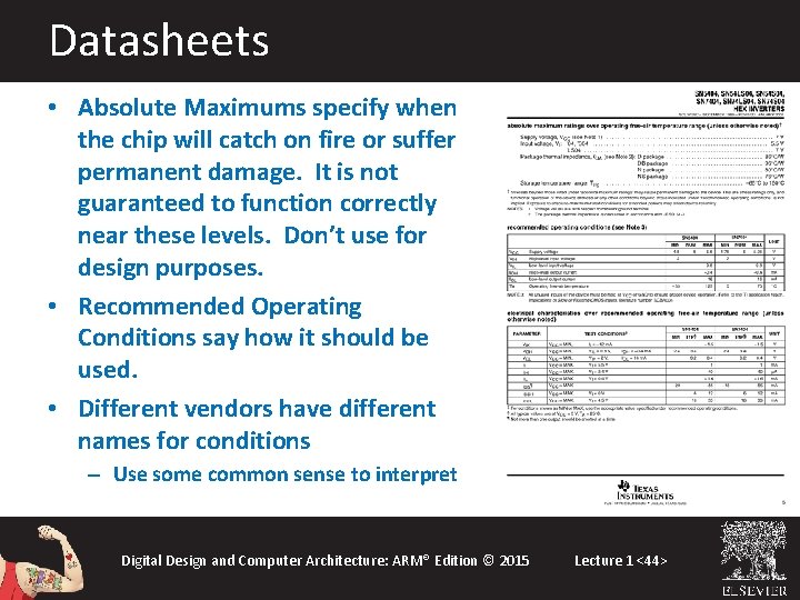
Datasheets • Absolute Maximums specify when the chip will catch on fire or suffer permanent damage. It is not guaranteed to function correctly near these levels. Don’t use for design purposes. • Recommended Operating Conditions say how it should be used. • Different vendors have different names for conditions – Use some common sense to interpret Digital Design and Computer Architecture: ARM® Edition © 2015 Lecture 1 <44>

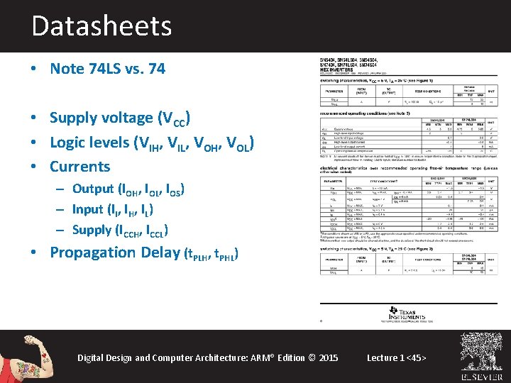
Datasheets • Note 74 LS vs. 74 • Supply voltage (VCC) • Logic levels (VIH, VIL, VOH, VOL) • Currents – Output (IOH, IOL, IOS) – Input (II, IH, IL) – Supply (ICCH, ICCL) • Propagation Delay (t. PLH, t. PHL) Digital Design and Computer Architecture: ARM® Edition © 2015 Lecture 1 <45>

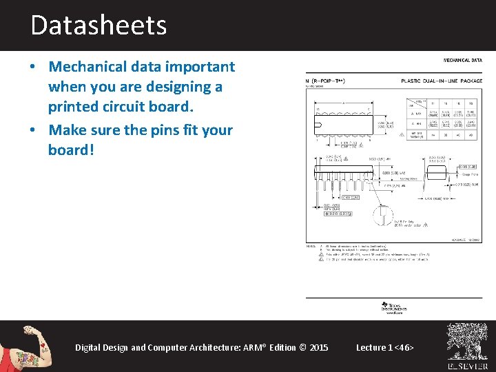
Datasheets • Mechanical data important when you are designing a printed circuit board. • Make sure the pins fit your board! Digital Design and Computer Architecture: ARM® Edition © 2015 Lecture 1 <46>

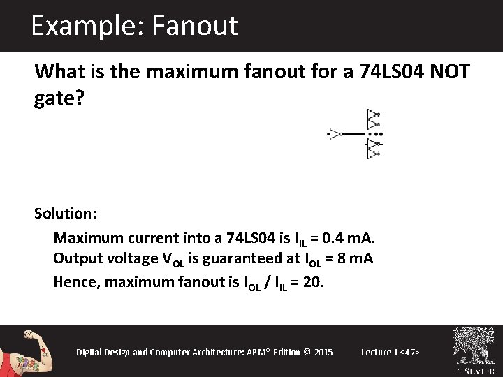
Example: Fanout What is the maximum fanout for a 74 LS 04 NOT gate? Solution: Maximum current into a 74 LS 04 is IIL = 0. 4 m. A. Output voltage VOL is guaranteed at IOL = 8 m. A Hence, maximum fanout is IOL / IIL = 20. Digital Design and Computer Architecture: ARM® Edition © 2015 Lecture 1 <47>

Example: Power Consumption One 74 LS 04 NOT gate drives 20 identical gates. VCC = 5 V. What is the power consumption of the entire system if the input to the first gate switches at 1 MHz? Static Power: Each gate draws ICC = (ICCL + ICCH)/2 = (6. 6 + 2. 4 m. A)/2 = 4. 5 m. A Istatic = (21 gates)(4. 5 m. A/gate) = 94. 5 m. A Pstatic = 94. 5 m. A * 5 V = 472. 5 m. W Dynamic Power Cin is not specified. Assume 15 p. F/gate * 20 gates = 300 p. F. P = CVDD 2 f = (300 x 10 -12)(52)(1 x 10⁶) = 7. 5 m. W Ptotal = Pstatic + Pdynamic = 480 m. W TTL power is primarily static Digital Design and Computer Architecture: ARM® Edition © 2015 Lecture 1 <48>