DYNAMIC SCAN CLOCK CONTROL FOR TEST TIME REDUCTION
- Slides: 14

DYNAMIC SCAN CLOCK CONTROL FOR TEST TIME REDUCTION MAINTAINING PEAK POWER LIMIT Priyadharshini Shanmugasundaram priyas@nvidia. com Vishwani D. Agrawal vagrawal@eng. auburn. edu

TESTING OF VLSI CIRCUITS - POWER AND TIME • High circuit activity during test • Functional slowdown and high test power dissipation • Peak power - Large IR drop in power distribution lines • Voltage droop and ground bounce (power supply noise) • Reduced voltage slows the gates down (delay fault) • Average power - Excessive heating • Timing failures • Permanent damage to circuit • Good chip may be labeled as bad → yield loss VTS’ 11 05/04/2011 2

TESTING OF VLSI CIRCUITS - POWER AND TIME • Existing solution: Use worst-case test clock rate • Keeps highest activity per unit time within specification • Keeps average and peak power within specification • Results in long test time VTS’ 11 05/04/2011 3

PROBLEM STATEMENT • Reduce test time without exceeding the power specification • Proposed solution: Adaptive test clock • Use worst-case clock rate when circuit activity is not known • Monitor circuit activity and speed up the clock when activity reduces VTS’ 11 05/04/2011 4

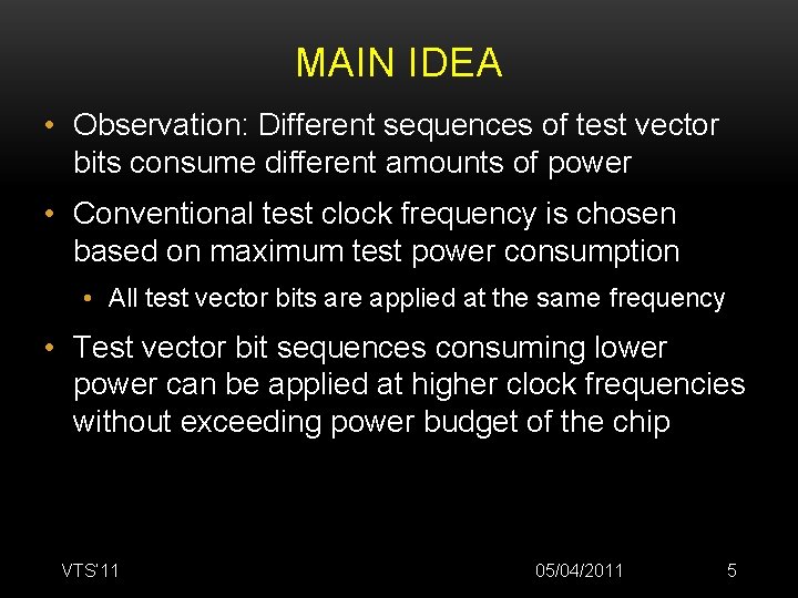
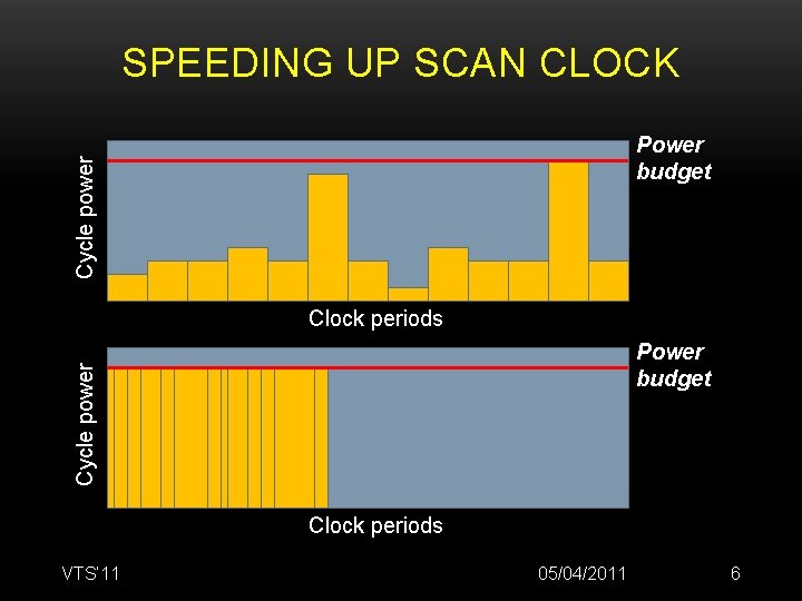
MAIN IDEA • Observation: Different sequences of test vector bits consume different amounts of power • Conventional test clock frequency is chosen based on maximum test power consumption • All test vector bits are applied at the same frequency • Test vector bit sequences consuming lower power can be applied at higher clock frequencies without exceeding power budget of the chip VTS’ 11 05/04/2011 5

SPEEDING UP SCAN CLOCK Cycle power Power budget Clock periods VTS’ 11 05/04/2011 6

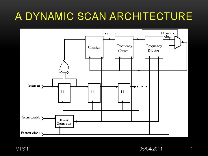
A DYNAMIC SCAN ARCHITECTURE VTS’ 11 05/04/2011 7

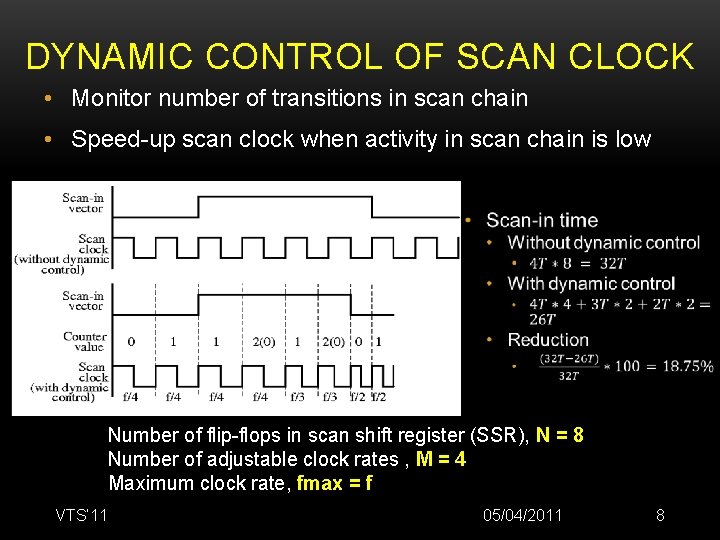
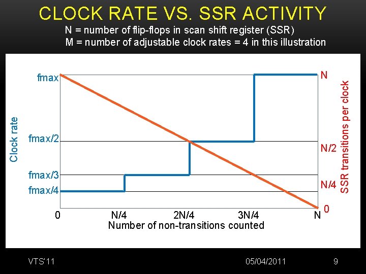
DYNAMIC CONTROL OF SCAN CLOCK • Monitor number of transitions in scan chain • Speed-up scan clock when activity in scan chain is low Number of flip-flops in scan shift register (SSR), N = 8 Number of adjustable clock rates , M = 4 Maximum clock rate, fmax = f VTS’ 11 05/04/2011 8

CLOCK RATE VS. SSR ACTIVITY N Clock rate fmax/2 N/2 fmax/3 fmax/4 0 VTS’ 11 N/4 2 N/4 3 N/4 Number of non-transitions counted 05/04/2011 0 N 9 SSR transitions per clock N = number of flip-flops in scan shift register (SSR) M = number of adjustable clock rates = 4 in this illustration

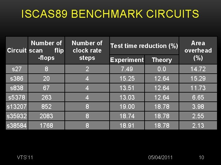
ISCAS 89 BENCHMARK CIRCUITS Number of Circuit scan flip -flops Number of clock rate steps Experiment Theory Area overhead (%) Test time reduction (%) s 27 8 2 7. 49 0. 0 14. 72 s 386 20 4 15. 25 12. 64 15. 29 s 838 67 4 13. 51 12. 64 11. 73 s 5378 263 4 13. 03 12. 64 6. 65 s 13207 852 8 19. 00 18. 78 3. 98 s 35932 2083 8 18. 74 18. 78 2. 55 s 38584 1768 8 18. 91 18. 78 2. 13 VTS’ 11 05/04/2011 10

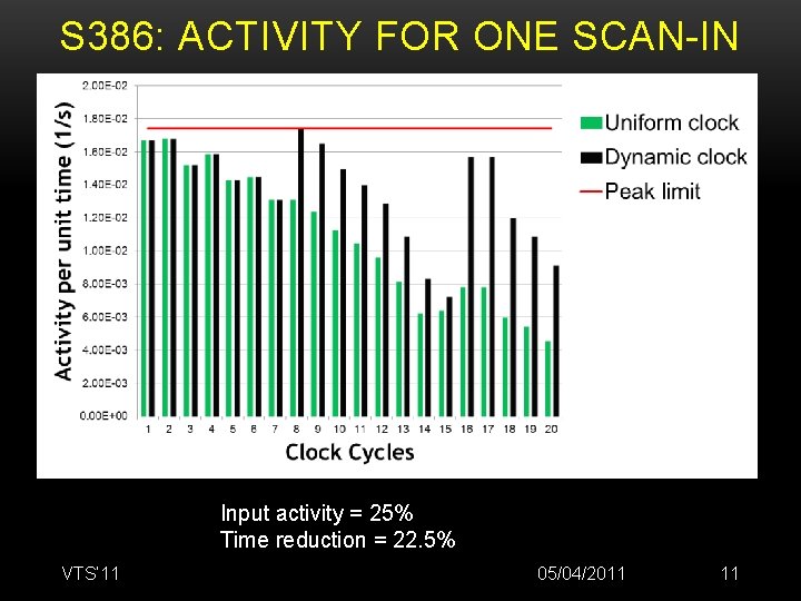
S 386: ACTIVITY FOR ONE SCAN-IN Input activity = 25% Time reduction = 22. 5% VTS’ 11 05/04/2011 11

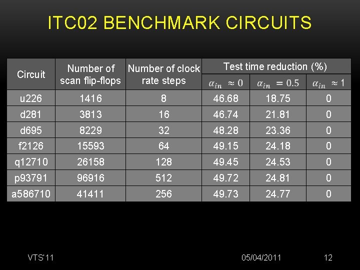
ITC 02 BENCHMARK CIRCUITS Circuit Number of clock scan flip-flops rate steps Test time reduction (%) u 226 1416 8 46. 68 18. 75 0 d 281 3813 16 46. 74 21. 81 0 d 695 8229 32 48. 28 23. 36 0 f 2126 15593 64 49. 15 24. 18 0 q 12710 26158 128 49. 45 24. 53 0 p 93791 96916 512 49. 72 24. 81 0 a 586710 41411 256 49. 73 24. 77 0 VTS’ 11 05/04/2011 12

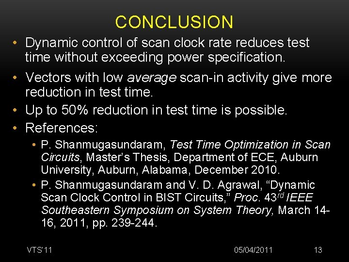
CONCLUSION • Dynamic control of scan clock rate reduces test time without exceeding power specification. • Vectors with low average scan-in activity give more reduction in test time. • Up to 50% reduction in test time is possible. • References: • P. Shanmugasundaram, Test Time Optimization in Scan Circuits, Master’s Thesis, Department of ECE, Auburn University, Auburn, Alabama, December 2010. • P. Shanmugasundaram and V. D. Agrawal, “Dynamic Scan Clock Control in BIST Circuits, ” Proc. 43 rd IEEE Southeastern Symposium on System Theory, March 1416, 2011, pp. 239 -244. VTS’ 11 05/04/2011 13

QUESTIONS? VTS’ 11 05/04/2011 14