DSP C 5000 Chapter 3 Addressing Modes Copyright





![Example System Diagram DROM RAM tbl[3] x[3] EPROM 54 x CPU code ESIEE, Slide Example System Diagram DROM RAM tbl[3] x[3] EPROM 54 x CPU code ESIEE, Slide](https://slidetodoc.com/presentation_image_h/bac955879e973ae8a9cf32eee415a371/image-37.jpg)
![Example + + ROM RAM tbl[4] x[4] y = x 0 + x 1 Example + + ROM RAM tbl[4] x[4] y = x 0 + x 1](https://slidetodoc.com/presentation_image_h/bac955879e973ae8a9cf32eee415a371/image-56.jpg)
![Example ROM RAM tbl[4] x[4] y = x 0 + x 1 + x Example ROM RAM tbl[4] x[4] y = x 0 + x 1 + x](https://slidetodoc.com/presentation_image_h/bac955879e973ae8a9cf32eee415a371/image-63.jpg)


- Slides: 73

DSP C 5000 Chapter 3 Addressing Modes Copyright © 2003 Texas Instruments. All rights reserved.

Objectives ESIEE, Slide 2 Present the main addressing modes and allocation of sections Present the main addressing modes of the C 54 family Present the main addressing modes of the C 55 family Explain how to use these addressing modes Do exercises to practice using the different addressing modes

Outline Generalities on addressing modes C 54 x C 55 x ESIEE, Slide 3

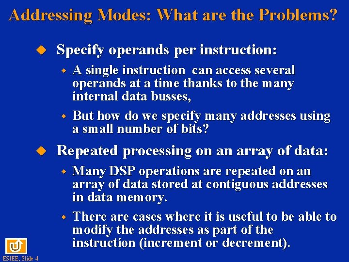
Addressing Modes: What are the Problems? Specify operands per instruction: w w Repeated processing on an array of data: w w ESIEE, Slide 4 A single instruction can access several operands at a time thanks to the many internal data busses, But how do we specify many addresses using a small number of bits? Many DSP operations are repeated on an array of data stored at contiguous addresses in data memory. There are cases where it is useful to be able to modify the addresses as part of the instruction (increment or decrement).

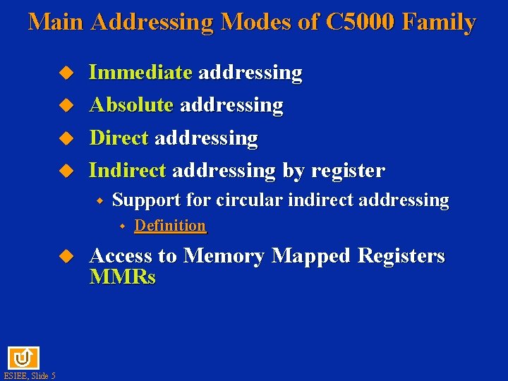
Main Addressing Modes of C 5000 Family Immediate addressing Absolute addressing Direct addressing Indirect addressing by register w Support for circular indirect addressing w ESIEE, Slide 5 Definition Access to Memory Mapped Registers MMRs

Allocating Sections ESIEE, Slide 6

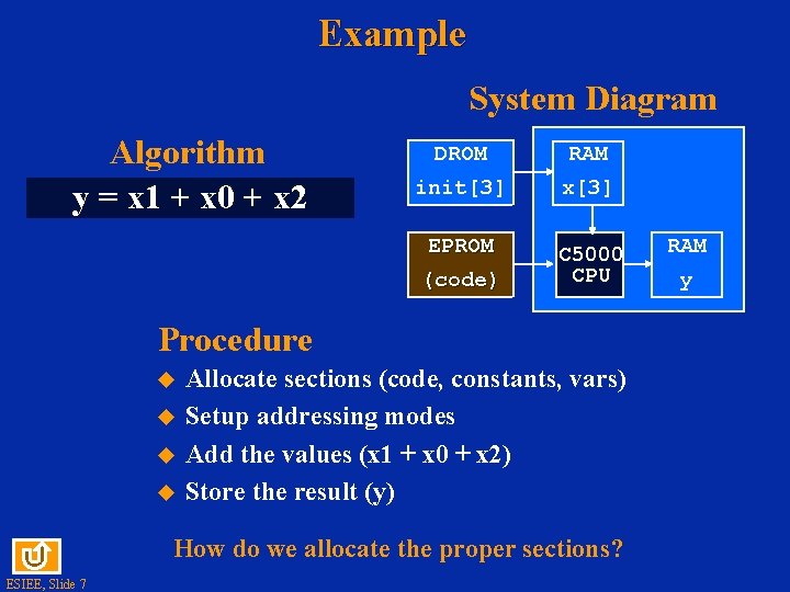
Example System Diagram Algorithm y = x 1 + x 0 + x 2 DROM RAM init[3] x[3] EPROM C 5000 CPU (code) Procedure Allocate sections (code, constants, vars) Setup addressing modes Add the values (x 1 + x 0 + x 2) Store the result (y) How do we allocate the proper sections? ESIEE, Slide 7 RAM y

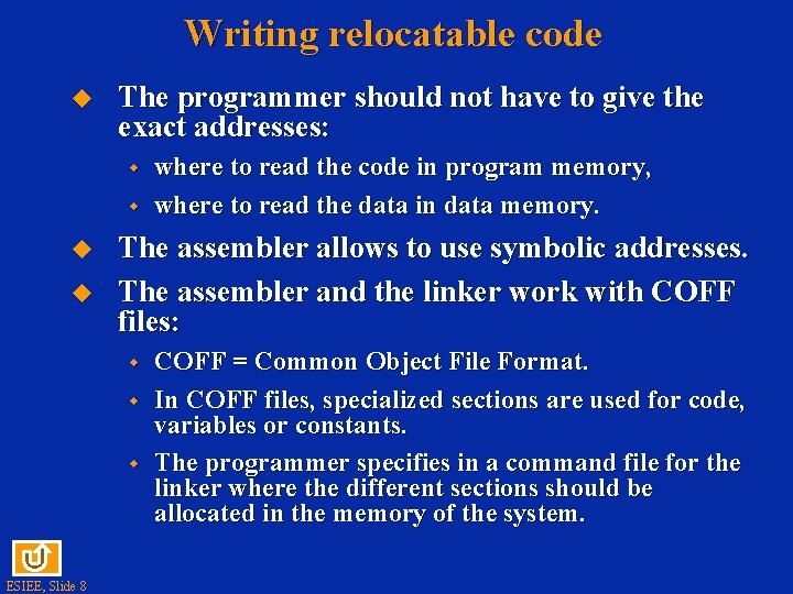
Writing relocatable code The programmer should not have to give the exact addresses: w w The assembler allows to use symbolic addresses. The assembler and the linker work with COFF files: w w w ESIEE, Slide 8 where to read the code in program memory, where to read the data in data memory. COFF = Common Object File Format. In COFF files, specialized sections are used for code, variables or constants. The programmer specifies in a command file for the linker where the different sections should be allocated in the memory of the system.

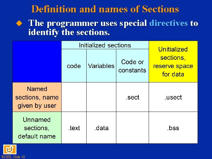
Definition of Sections Different sections for code, vars, constants. The sections can be initialized or not. w w ESIEE, Slide 9 An initialized section is filled with code or constant values. An uninitialized section reserves memory space for a variable. The sections can have default names or names given by the programmer.

Definition and names of Sections ESIEE, Slide 10 The programmer uses special directives to identify the sections.

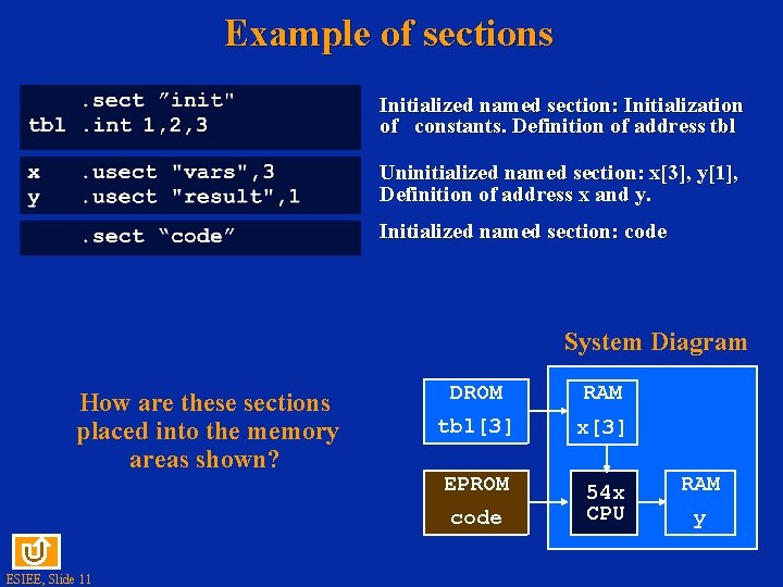
Example of sections Initialized named section: Initialization of constants. Definition of address tbl Uninitialized named section: x[3], y[1], Definition of address x and y. Initialized named section: code System Diagram How are these sections placed into the memory areas shown? DROM RAM tbl[3] x[3] EPROM 54 x CPU code ESIEE, Slide 11 RAM y

C 54 x Addressing Modes ESIEE, Slide 12

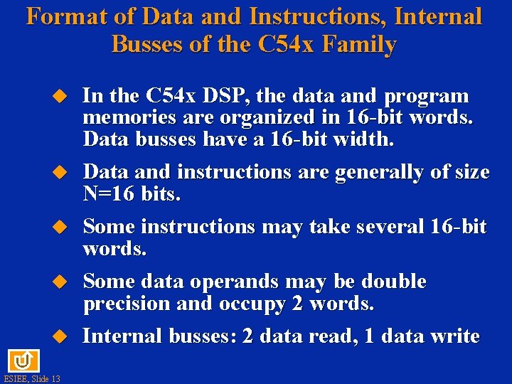
Format of Data and Instructions, Internal Busses of the C 54 x Family ESIEE, Slide 13 In the C 54 x DSP, the data and program memories are organized in 16 -bit words. Data busses have a 16 -bit width. Data and instructions are generally of size N=16 bits. Some instructions may take several 16 -bit words. Some data operands may be double precision and occupy 2 words. Internal busses: 2 data read, 1 data write

Terms from the User’s Guide ESIEE, Slide 14

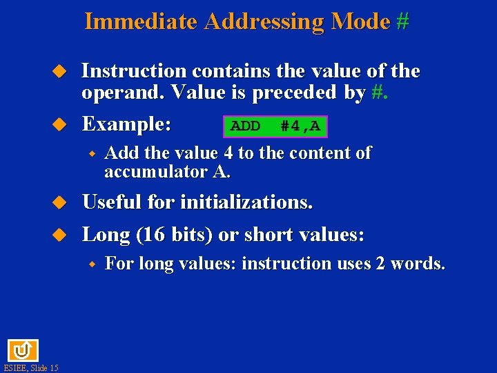
Immediate Addressing Mode # Instruction contains the value of the operand. Value is preceded by #. ADD #4, A Example: w Useful for initializations. Long (16 bits) or short values: w ESIEE, Slide 15 Add the value 4 to the content of accumulator A. For long values: instruction uses 2 words.

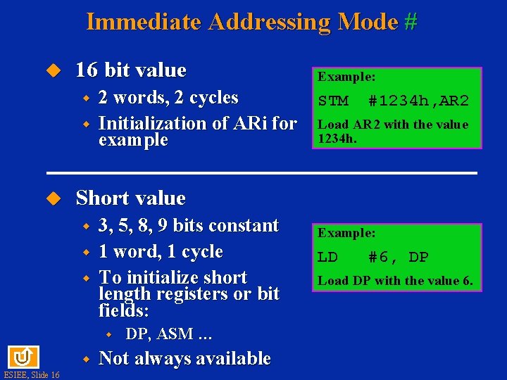
Immediate Addressing Mode # 16 bit value w w 2 words, 2 cycles STM #1234 h, AR 2 Initialization of ARi for Load AR 2 with the value 1234 h. example Short value w w w 3, 5, 8, 9 bits constant 1 word, 1 cycle To initialize short length registers or bit fields: w w ESIEE, Slide 16 Example: DP, ASM … Not always available Example: LD #6, DP Load DP with the value 6.

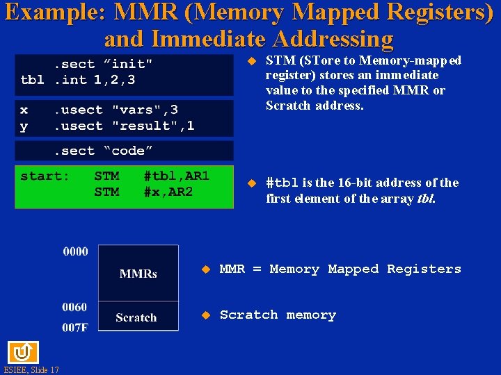
Example: MMR (Memory Mapped Registers) and Immediate Addressing ESIEE, Slide 17 STM (STore to Memory-mapped register) stores an immediate value to the specified MMR or Scratch address. #tbl is the 16 -bit address of the first element of the array tbl. MMR = Memory Mapped Registers Scratch memory

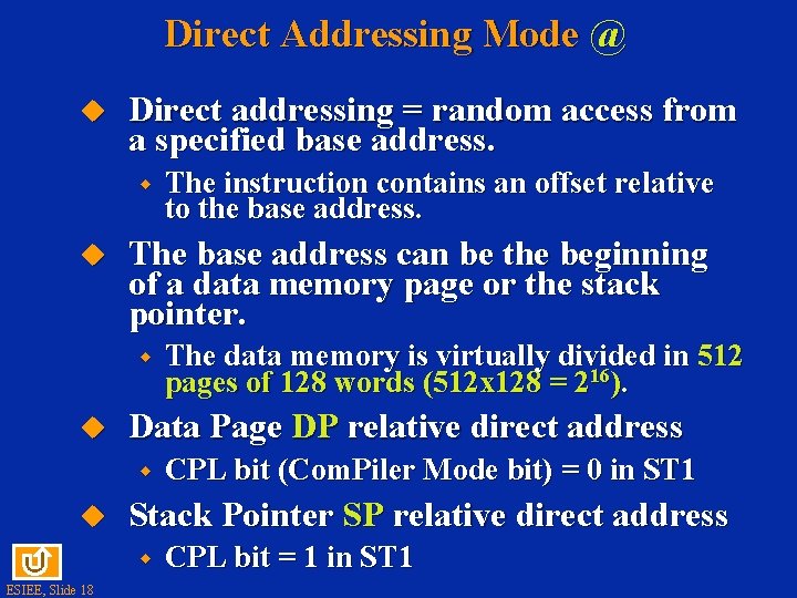
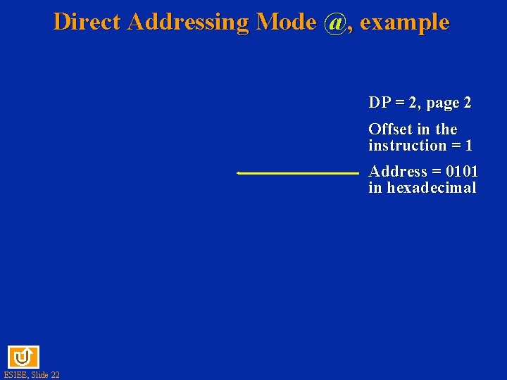
Direct Addressing Mode @ Direct addressing = random access from a specified base address. w The base address can be the beginning of a data memory page or the stack pointer. w CPL bit (Com. Piler Mode bit) = 0 in ST 1 Stack Pointer SP relative direct address w ESIEE, Slide 18 The data memory is virtually divided in 512 pages of 128 words (512 x 128 = 216). Data Page DP relative direct address w The instruction contains an offset relative to the base address. CPL bit = 1 in ST 1

Data memory pages ESIEE, Slide 19

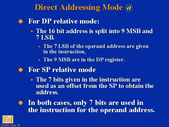
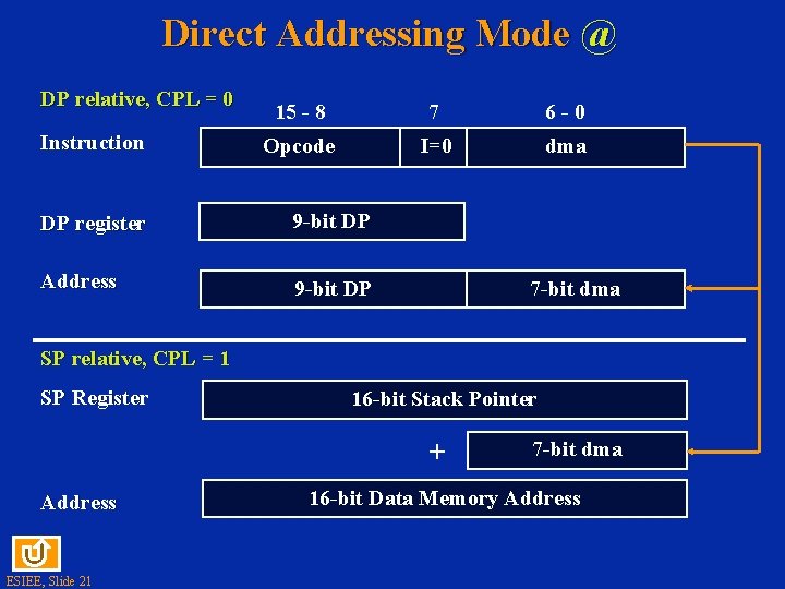
Direct Addressing Mode @ For DP relative mode: w The 16 bit address is split into 9 MSB and 7 LSB. w w For SP relative mode w ESIEE, Slide 20 The 7 LSB of the operand address are given in the instruction, The 9 MSB are in the DP register. The 7 bits given in the instruction are used as an offset from the SP to obtain the address. In both cases, only 7 bits are used in the instruction for the operand address.

Direct Addressing Mode @ DP relative, CPL = 0 Instruction 15 - 8 7 6 -0 Opcode I=0 dma DP register 9 -bit DP Address 9 -bit DP 7 -bit dma SP relative, CPL = 1 SP Register 16 -bit Stack Pointer + Address ESIEE, Slide 21 7 -bit dma 16 -bit Data Memory Address

Direct Addressing Mode @, example DP = 2, page 2 Offset in the instruction = 1 Address = 0101 in hexadecimal ESIEE, Slide 22

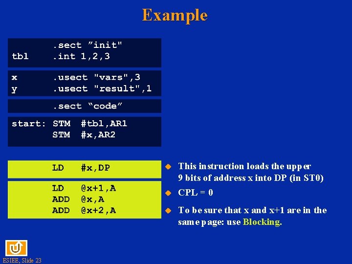
Example ESIEE, Slide 23 This instruction loads the upper 9 bits of address x into DP (in ST 0) CPL = 0 To be sure that x and x+1 are in the same page: use Blocking.

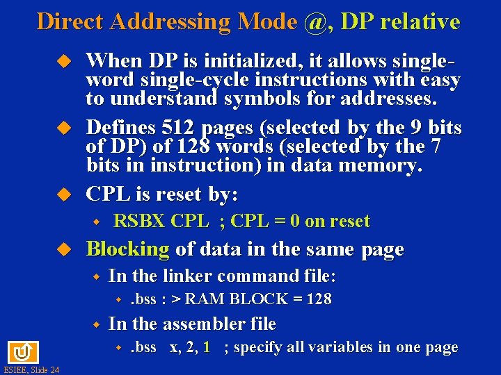
Direct Addressing Mode @, DP relative When DP is initialized, it allows singleword single-cycle instructions with easy to understand symbols for addresses. Defines 512 pages (selected by the 9 bits of DP) of 128 words (selected by the 7 bits in instruction) in data memory. CPL is reset by: w RSBX CPL ; CPL = 0 on reset Blocking of data in the same page w In the linker command file: w w In the assembler file w ESIEE, Slide 24 . bss : > RAM BLOCK = 128. bss x, 2, 1 ; specify all variables in one page

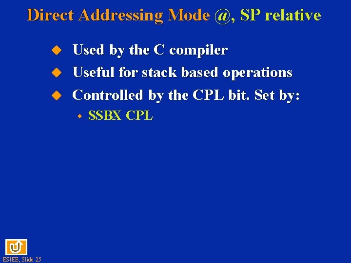
Direct Addressing Mode @, SP relative Used by the C compiler Useful for stack based operations Controlled by the CPL bit. Set by: w ESIEE, Slide 25 SSBX CPL

Indirect Addressing Mode *ARi ESIEE, Slide 26 Compatible with pointers in C. 8 ARi Auxiliary Registers to store the addresses of the operands. They are used as pointers. 2 ARAU = Auxiliary Registers Arithmetic Units to realize operations on the addresses stored in the ARi. 1 operand (Smem) or 2 operands (Xmem, Ymem) can be specified by indirect addressing in 1 instruction. Very efficient for DSP operations.

Indirect addressing mode *ARi AR 0 can be used as an index. Support for circular addressing w Bit Reversed BR addressing for FFT ARi can be modified during the instruction w ESIEE, Slide 27 details in next slides The possible modifications or operations on ARi depend on the number of operands specified by indirect addressing in the instruction. Pointers (ARi) must be initialized before use.

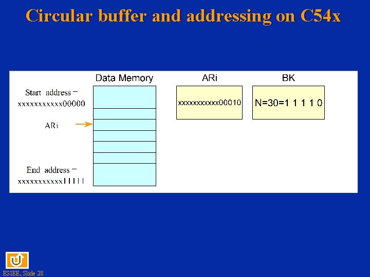
Circular buffer and addressing on C 54 x ESIEE, Slide 28

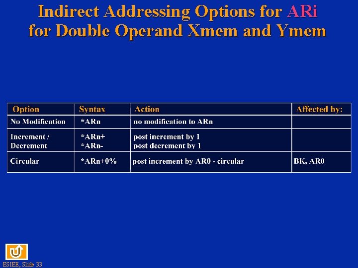
Circular addressing with C 54 x Circular indirect addressing mode: % w w *ARi-%, *ARi+%, *ARi-0%, *ARi+0%, *ARi(lk)% In dual operand mode Xmem, Ymem: w w BK register: w w w ESIEE, Slide 29 *ARi+0% only valid mode To perform a decrement, store a negative value in AR 0. Stores the size N of the circular buffer. Must be initialized before use. There may be several circular buffers at different addresses at the same time but with the same length.

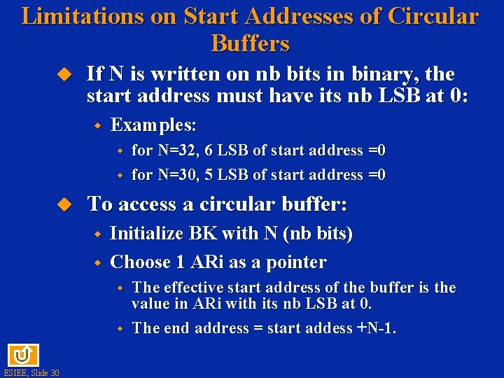
Limitations on Start Addresses of Circular Buffers If N is written on nb bits in binary, the start address must have its nb LSB at 0: w Examples: w w To access a circular buffer: w w Initialize BK with N (nb bits) Choose 1 ARi as a pointer w w ESIEE, Slide 30 for N=32, 6 LSB of start address =0 for N=30, 5 LSB of start address =0 The effective start address of the buffer is the value in ARi with its nb LSB at 0. The end address = start addess +N-1.

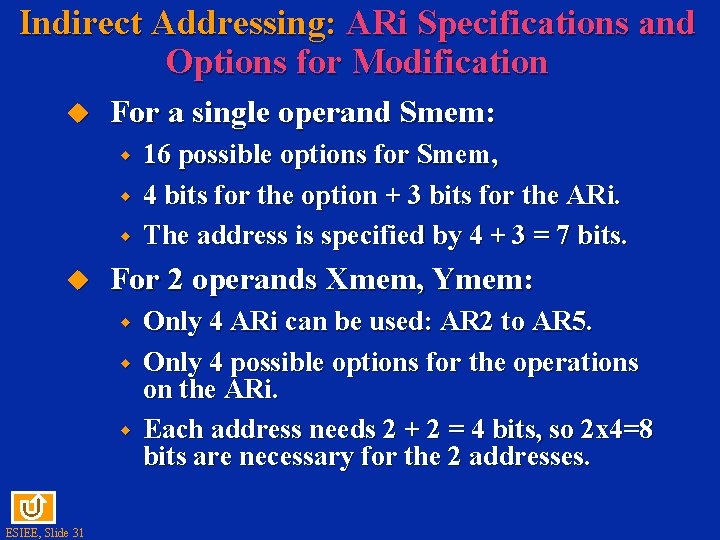
Indirect Addressing: ARi Specifications and Options for Modification For a single operand Smem: w w w For 2 operands Xmem, Ymem: w w w ESIEE, Slide 31 16 possible options for Smem, 4 bits for the option + 3 bits for the ARi. The address is specified by 4 + 3 = 7 bits. Only 4 ARi can be used: AR 2 to AR 5. Only 4 possible options for the operations on the ARi. Each address needs 2 + 2 = 4 bits, so 2 x 4=8 bits are necessary for the 2 addresses.

Indirect Addressing Options for ARi modifications, Single operand Smem ESIEE, Slide 32

Indirect Addressing Options for ARi for Double Operand Xmem and Ymem ESIEE, Slide 33

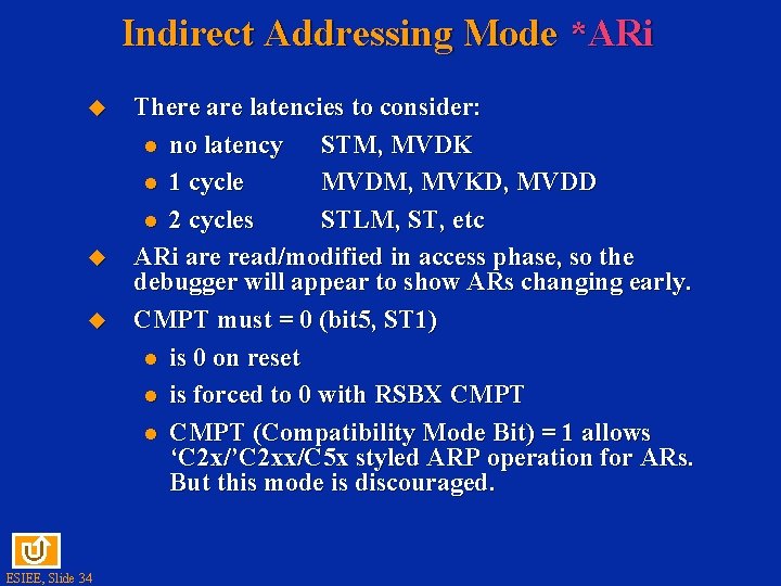
Indirect Addressing Mode *ARi ESIEE, Slide 34 There are latencies to consider: l no latency STM, MVDK l 1 cycle MVDM, MVKD, MVDD l 2 cycles STLM, ST, etc ARi are read/modified in access phase, so the debugger will appear to show ARs changing early. CMPT must = 0 (bit 5, ST 1) l is 0 on reset l is forced to 0 with RSBX CMPT l CMPT (Compatibility Mode Bit) = 1 allows ‘C 2 x/’C 2 xx/C 5 x styled ARP operation for ARs. But this mode is discouraged.

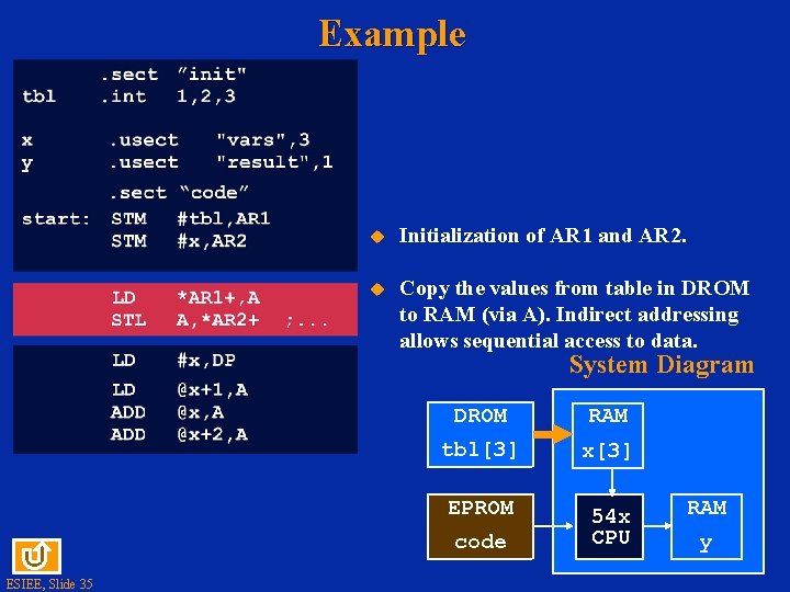
Example Initialization of AR 1 and AR 2. Copy the values from table in DROM to RAM (via A). Indirect addressing allows sequential access to data. System Diagram DROM RAM tbl[3] x[3] EPROM 54 x CPU code ESIEE, Slide 35 RAM y

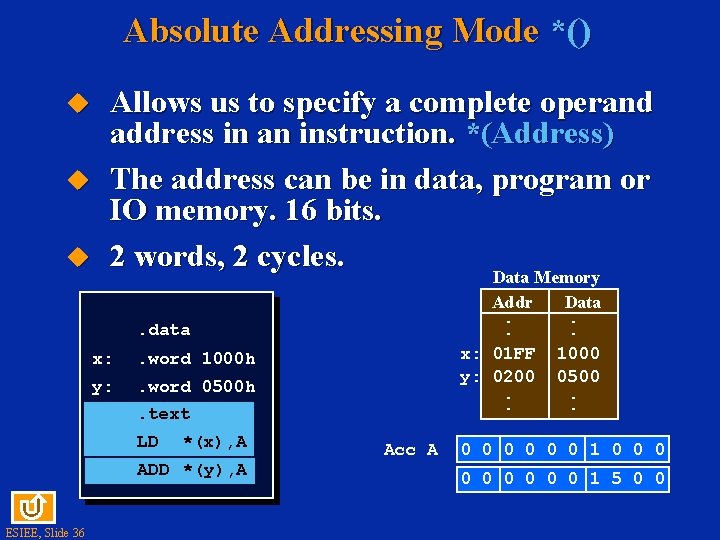
Absolute Addressing Mode *() Allows us to specify a complete operand address in an instruction. *(Address) The address can be in data, program or IO memory. 16 bits. 2 words, 2 cycles. Data Memory Addr. . x: 01 FF y: 0200. . . data x: . word 1000 h y: . word 0500 h. text LD *(x), A ADD *(y), A ESIEE, Slide 36 Acc A Data. . 1000 0500. . 0 0 0 1 0 0 0 0 0 1 5 0 0
![Example System Diagram DROM RAM tbl3 x3 EPROM 54 x CPU code ESIEE Slide Example System Diagram DROM RAM tbl[3] x[3] EPROM 54 x CPU code ESIEE, Slide](https://slidetodoc.com/presentation_image_h/bac955879e973ae8a9cf32eee415a371/image-37.jpg)
Example System Diagram DROM RAM tbl[3] x[3] EPROM 54 x CPU code ESIEE, Slide 37 RAM y Save accumulator A at address y

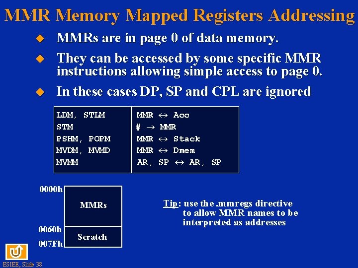
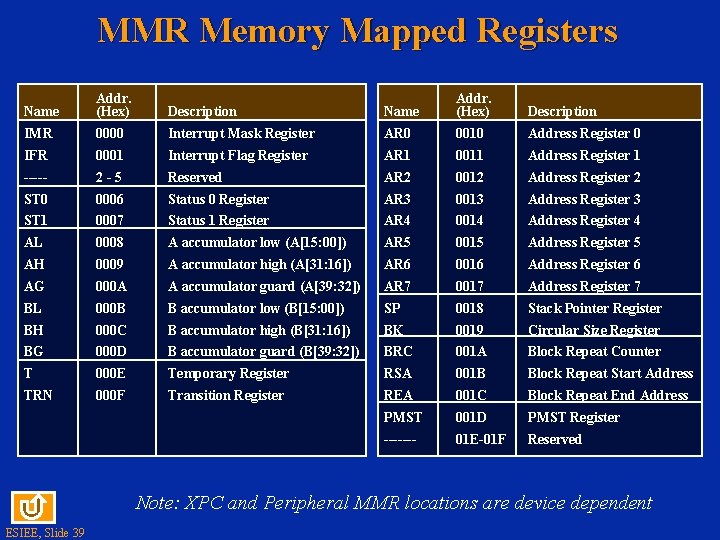
MMR Memory Mapped Registers Addressing MMRs are in page 0 of data memory. They can be accessed by some specific MMR instructions allowing simple access to page 0. In these cases DP, SP and CPL are ignored LDM, STLM STM PSHM, POPM MVDM, MVMD MVMM MMR # ® MMR AR, « Acc MMR « Stack « Dmem SP « AR, SP 0000 h MMRs 0060 h 007 Fh ESIEE, Slide 38 Scratch Tip: use the. mmregs directive to allow MMR names to be interpreted as addresses

MMR Memory Mapped Registers Name Addr. (Hex) Description IMR 0000 Interrupt Mask Register AR 0 0010 Address Register 0 IFR 0001 Interrupt Flag Register AR 1 0011 Address Register 1 ----- 2 -5 Reserved AR 2 0012 Address Register 2 ST 0 0006 Status 0 Register AR 3 0013 Address Register 3 ST 1 0007 Status 1 Register AR 4 0014 Address Register 4 AL 0008 A accumulator low (A[15: 00]) AR 5 0015 Address Register 5 AH 0009 A accumulator high (A[31: 16]) AR 6 0016 Address Register 6 AG 000 A A accumulator guard (A[39: 32]) AR 7 0017 Address Register 7 BL 000 B B accumulator low (B[15: 00]) SP 0018 Stack Pointer Register BH 000 C B accumulator high (B[31: 16]) BK 0019 Circular Size Register BG 000 D B accumulator guard (B[39: 32]) BRC 001 A Block Repeat Counter T 000 E Temporary Register RSA 001 B Block Repeat Start Address TRN 000 F Transition Register REA 001 C Block Repeat End Address PMST 001 D PMST Register ------- 01 E-01 F Reserved Note: XPC and Peripheral MMR locations are device dependent ESIEE, Slide 39

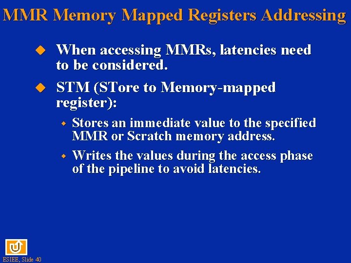
MMR Memory Mapped Registers Addressing When accessing MMRs, latencies need to be considered. STM (STore to Memory-mapped register): w w ESIEE, Slide 40 Stores an immediate value to the specified MMR or Scratch memory address. Writes the values during the access phase of the pipeline to avoid latencies.

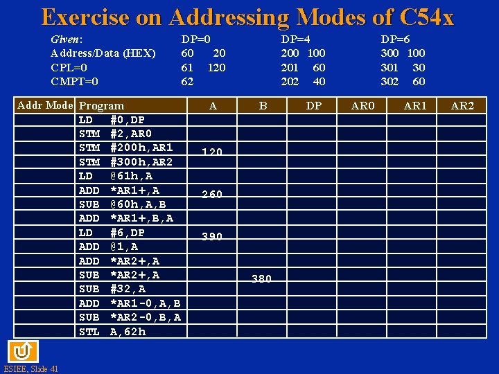
Exercise on Addressing Modes of C 54 x Given: Address/Data (HEX) CPL=0 CMPT=0 Addr Mode Program LD STM STM LD ADD SUB ADD SUB STL ESIEE, Slide 41 #0, DP #2, AR 0 #200 h, AR 1 #300 h, AR 2 @61 h, A *AR 1+, A @60 h, A, B *AR 1+, B, A #6, DP @1, A *AR 2+, A #32, A *AR 1 -0, A, B *AR 2 -0, B, A A, 62 h DP=0 60 20 61 120 62 A DP=4 200 100 201 60 202 40 B 120 260 390 380 DP DP=6 300 100 301 30 302 60 AR 1 AR 2

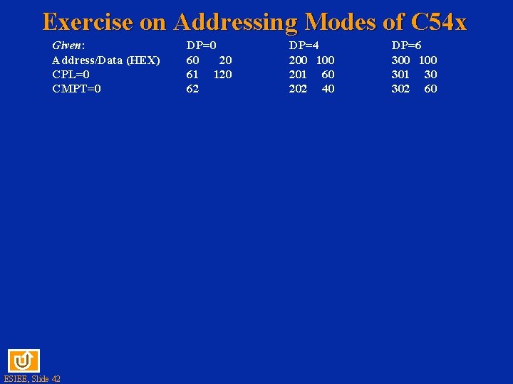
Exercise on Addressing Modes of C 54 x Given: Address/Data (HEX) CPL=0 CMPT=0 ESIEE, Slide 42 DP=0 60 20 61 120 62 DP=4 200 100 201 60 202 40 DP=6 300 100 301 30 302 60

C 55 x Addressing Modes ESIEE, Slide 43

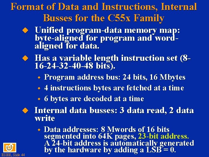
Format of Data and Instructions, Internal Busses for the C 55 x Family Unified program-data memory map: byte-aligned for program and wordaligned for data. Has a variable length instruction set (816 -24 -32 -40 -48 bits). w w w Internal data busses: 3 data read, 2 data write w ESIEE, Slide 44 Program address bus: 24 bits, 16 Mbytes 4 instructions bytes are fetched at a time 6 bytes are decoded at a time Data addresses: 8 Mwords of 16 bits segmented into 64 K pages, 23 -bit address. A 24 -bit address is automatically generated by the hardware by adding a LSB = 0.

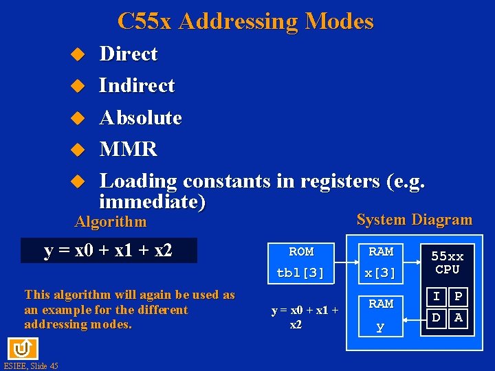
C 55 x Addressing Modes Direct Indirect Absolute MMR Loading constants in registers (e. g. immediate) System Diagram Algorithm y = x 0 + x 1 + x 2 This algorithm will again be used as an example for the different addressing modes. ESIEE, Slide 45 ROM RAM tbl[3] x[3] y = x 0 + x 1 + x 2 RAM y 55 xx CPU I P D A

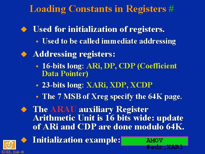
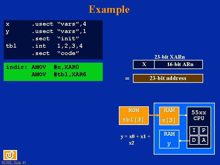
Loading Constants in Registers # Used for initialization of registers. w Addressing registers: w w w ESIEE, Slide 46 Used to be called immediate addressing 16 -bits long: ARi, DP, CDP (Coefficient Data Pointer) 23 -bits long: XARi, XDP, XCDP The 7 MSB of Xreg specify the 64 K page. The ARAU auxiliary Register Arithmetic Unit is 16 bits wide: update of ARi and CDP are done modulo 64 K. AMOV Initialization example: #adr, XAR 3

Example x y tbl . usect. int. sect indir: AMOV “vars”, 4 “vars”, 1 “init” 1, 2, 3, 4 “code” #x, XAR 0 #tbl, XAR 6 23 -bit XARn 16 -bit ARn X = 23 -bit address ROM RAM tbl[3] x[3] y = x 0 + x 1 + x 2 ESIEE, Slide 47 RAM y 55 xx CPU I P D A

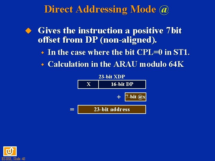
Direct Addressing Mode @ Gives the instruction a positive 7 bit offset from DP (non-aligned). w w In the case where the bit CPL=0 in ST 1. Calculation in the ARAU modulo 64 K X 23 -bit XDP 16 -bit DP + = ESIEE, Slide 48 7 -bit @x 23 -bit address

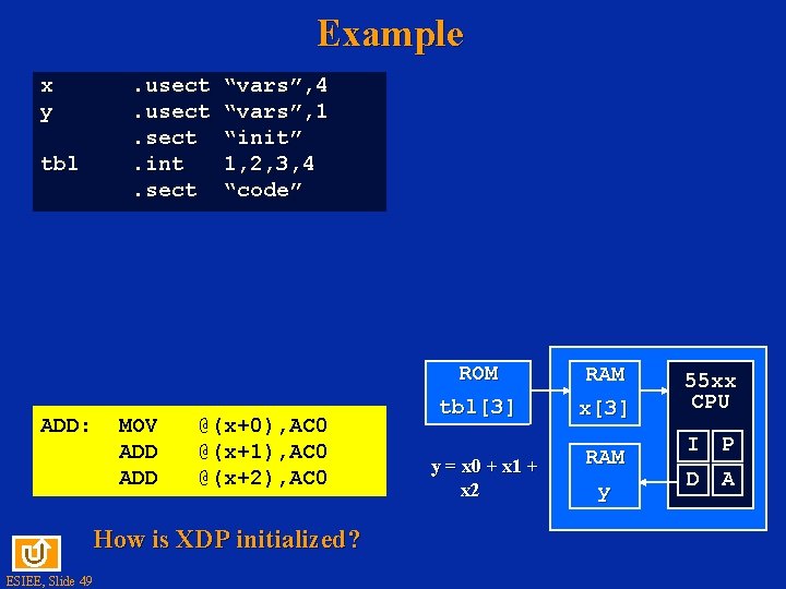
Example x y . usect. int. sect tbl ADD: MOV ADD “vars”, 4 “vars”, 1 “init” 1, 2, 3, 4 “code” @(x+0), AC 0 @(x+1), AC 0 @(x+2), AC 0 How is XDP initialized? ESIEE, Slide 49 ROM RAM tbl[3] x[3] y = x 0 + x 1 + x 2 RAM y 55 xx CPU I P D A

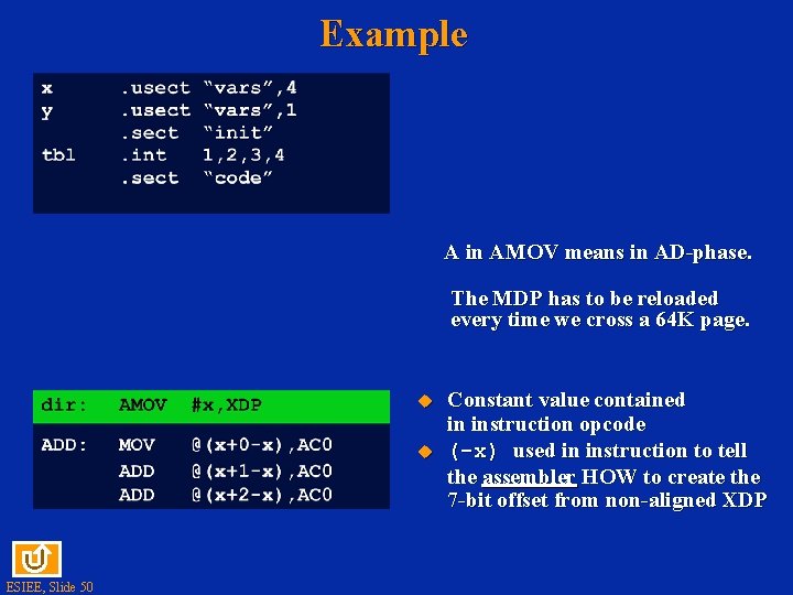
Example A in AMOV means in AD-phase. The MDP has to be reloaded every time we cross a 64 K page. ESIEE, Slide 50 Constant value contained in instruction opcode (-x) used in instruction to tell the assembler HOW to create the 7 -bit offset from non-aligned XDP

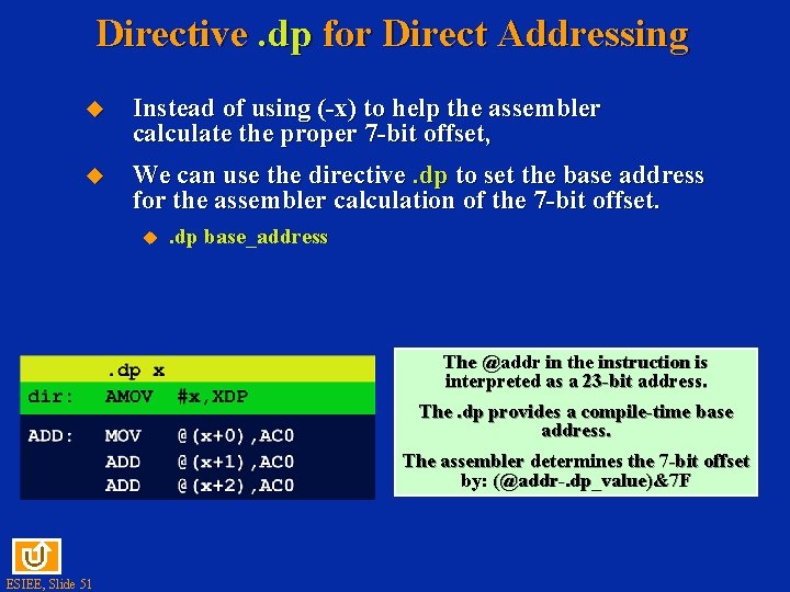
Directive. dp for Direct Addressing Instead of using (-x) to help the assembler calculate the proper 7 -bit offset, We can use the directive. dp to set the base address for the assembler calculation of the 7 -bit offset. . dp base_address The @addr in the instruction is interpreted as a 23 -bit address. The. dp provides a compile-time base address. The assembler determines the 7 -bit offset by: (@addr-. dp_value)&7 F ESIEE, Slide 51

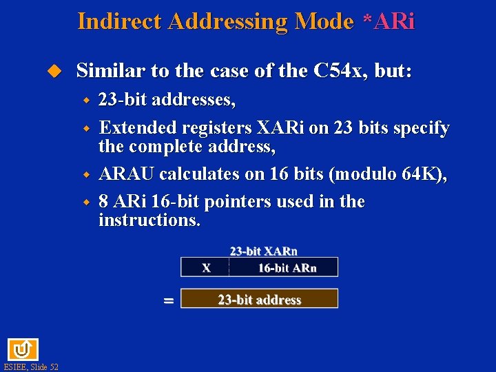
Indirect Addressing Mode *ARi Similar to the case of the C 54 x, but: w w ESIEE, Slide 52 23 -bit addresses, Extended registers XARi on 23 bits specify the complete address, ARAU calculates on 16 bits (modulo 64 K), 8 ARi 16 -bit pointers used in the instructions.

Indirect Addressing Options for Pointer ARi Modifications Assumes ST 2_55 ARMS=0 and ST 1_55 C 54 CM=0. The reset condition is C 54 CM=1. ESIEE, Slide 53

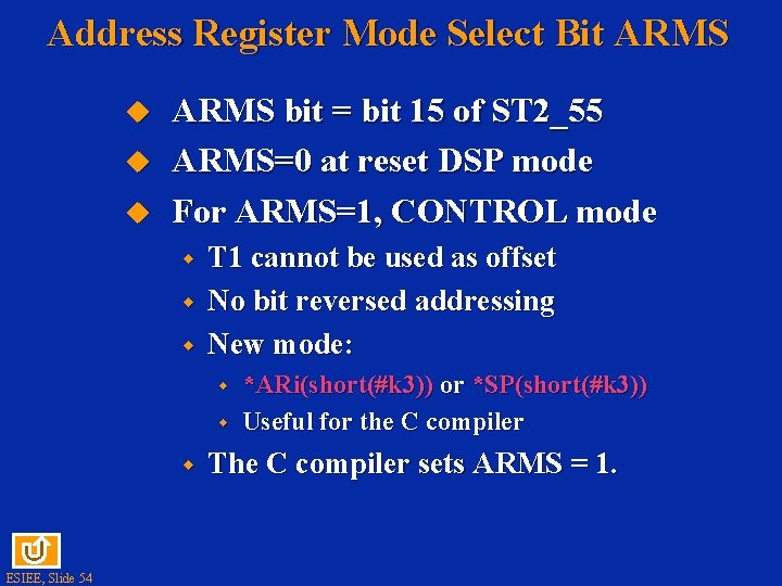
Address Register Mode Select Bit ARMS bit = bit 15 of ST 2_55 ARMS=0 at reset DSP mode For ARMS=1, CONTROL mode w w w T 1 cannot be used as offset No bit reversed addressing New mode: w w w ESIEE, Slide 54 *ARi(short(#k 3)) or *SP(short(#k 3)) Useful for the C compiler The C compiler sets ARMS = 1.

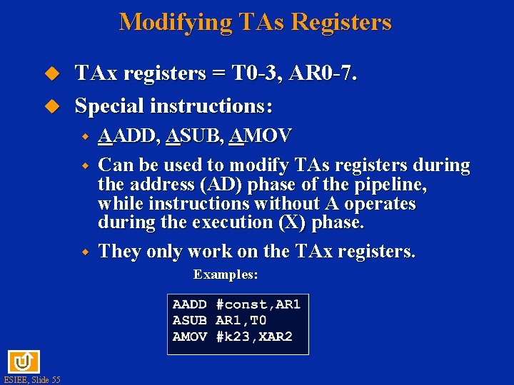
Modifying TAs Registers TAx registers = T 0 -3, AR 0 -7. Special instructions: w w w AADD, ASUB, AMOV Can be used to modify TAs registers during the address (AD) phase of the pipeline, while instructions without A operates during the execution (X) phase. They only work on the TAx registers. Examples: ESIEE, Slide 55
![Example ROM RAM tbl4 x4 y x 0 x 1 Example + + ROM RAM tbl[4] x[4] y = x 0 + x 1](https://slidetodoc.com/presentation_image_h/bac955879e973ae8a9cf32eee415a371/image-56.jpg)
Example + + ROM RAM tbl[4] x[4] y = x 0 + x 1 ESIEE, Slide 56 RAM y 55 xx CPU I P D A

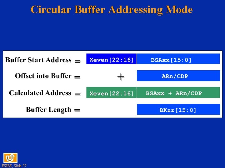
Circular Buffer Addressing Mode ESIEE, Slide 57

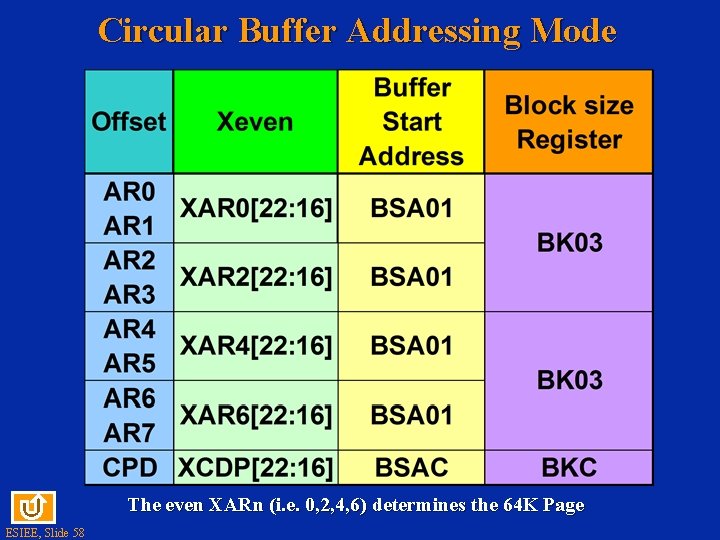
Circular Buffer Addressing Mode The even XARn (i. e. 0, 2, 4, 6) determines the 64 K Page ESIEE, Slide 58

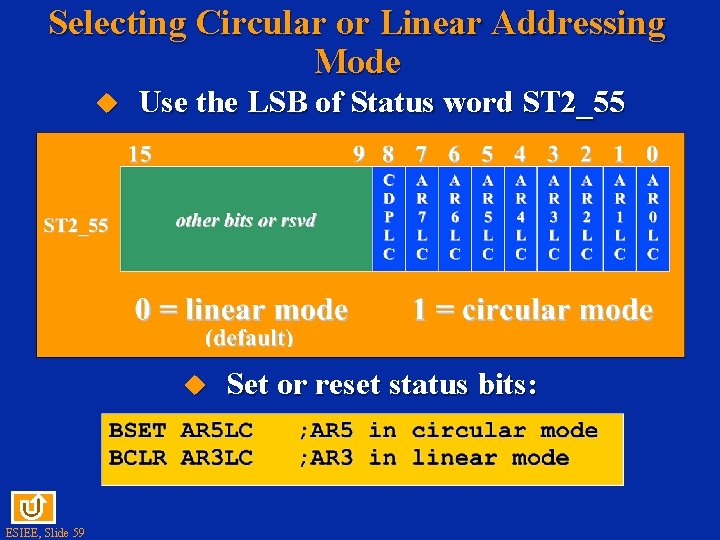
Selecting Circular or Linear Addressing Mode Use the LSB of Status word ST 2_55 ESIEE, Slide 59 Set or reset status bits:

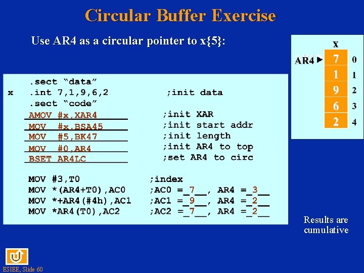
Circular Buffer Exercise Use AR 4 as a circular pointer to x{5}: Results are cumulative ESIEE, Slide 60

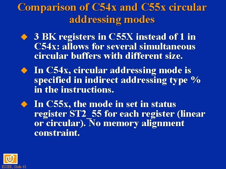
Comparison of C 54 x and C 55 x circular addressing modes ESIEE, Slide 61 3 BK registers in C 55 X instead of 1 in C 54 x: allows for several simultaneous circular buffers with different size. In C 54 x, circular addressing mode is specified in indirect addressing type % in the instructions. In C 55 x, the mode in set in status register ST 2_55 for each register (linear or circular). No memory alignment constraint.

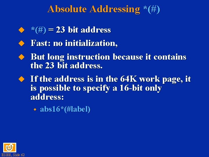
Absolute Addressing *(#) = 23 bit address Fast: no initialization, But long instruction because it contains the 23 bit address. If the address is in the 64 K work page, it is possible to specify a 16 -bit only address: w ESIEE, Slide 62 abs 16*(#label)
![Example ROM RAM tbl4 x4 y x 0 x 1 x Example ROM RAM tbl[4] x[4] y = x 0 + x 1 + x](https://slidetodoc.com/presentation_image_h/bac955879e973ae8a9cf32eee415a371/image-63.jpg)
Example ROM RAM tbl[4] x[4] y = x 0 + x 1 + x 2 ESIEE, Slide 63 RAM y 55 xx CPU I P D A

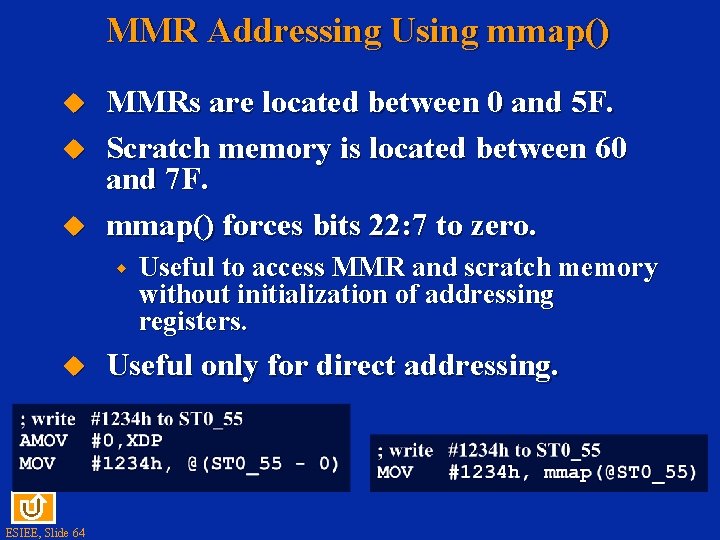
MMR Addressing Using mmap() MMRs are located between 0 and 5 F. Scratch memory is located between 60 and 7 F. mmap() forces bits 22: 7 to zero. w ESIEE, Slide 64 Useful to access MMR and scratch memory without initialization of addressing registers. Useful only for direct addressing.

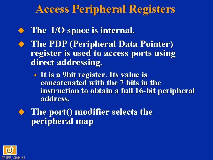
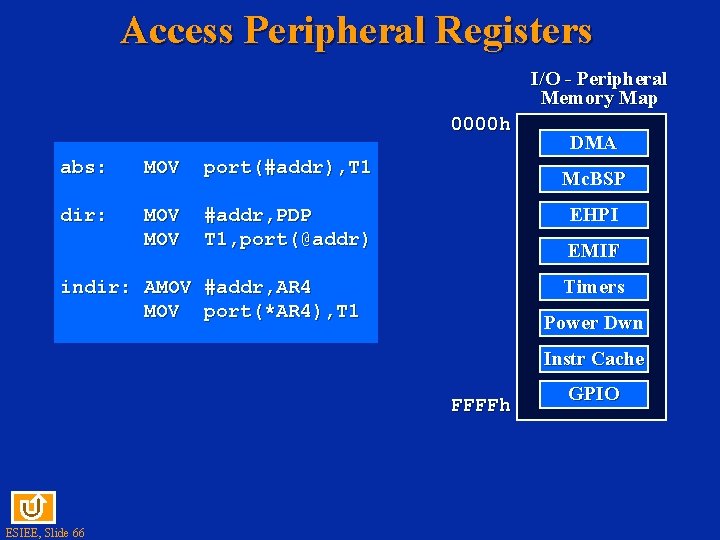
Access Peripheral Registers The I/O space is internal. The PDP (Peripheral Data Pointer) register is used to access ports using direct addressing. w ESIEE, Slide 65 It is a 9 bit register. Its value is concatenated with the 7 bits in the instruction to obtain a full 16 -bit peripheral address. The port() modifier selects the peripheral map

Access Peripheral Registers I/O - Peripheral Memory Map 0000 h abs: MOV port(#addr), T 1 dir: MOV #addr, PDP T 1, port(@addr) DMA Mc. BSP EHPI EMIF Timers indir: AMOV #addr, AR 4 MOV port(*AR 4), T 1 Power Dwn Instr Cache FFFFh ESIEE, Slide 66 GPIO

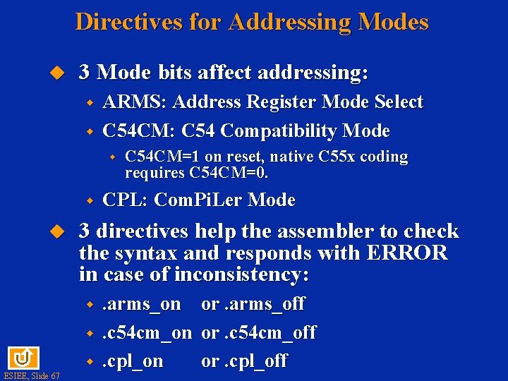
Directives for Addressing Modes 3 Mode bits affect addressing: w w ARMS: Address Register Mode Select C 54 CM: C 54 Compatibility Mode w w CPL: Com. Pi. Ler Mode 3 directives help the assembler to check the syntax and responds with ERROR in case of inconsistency: w w w ESIEE, Slide 67 C 54 CM=1 on reset, native C 55 x coding requires C 54 CM=0. . arms_on. c 54 cm_on. cpl_on or. arms_off or. c 54 cm_off or. cpl_off

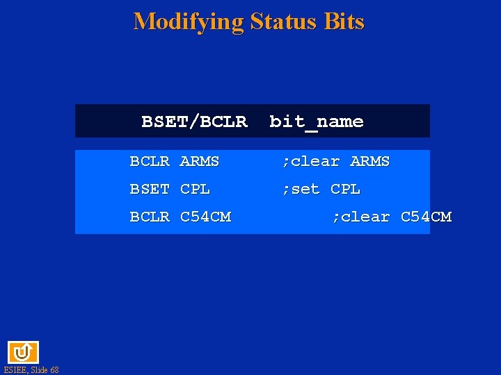
Modifying Status Bits BSET/BCLR ARMS ; clear ARMS BSET CPL ; set CPL BCLR C 54 CM ESIEE, Slide 68 bit_name ; clear C 54 CM

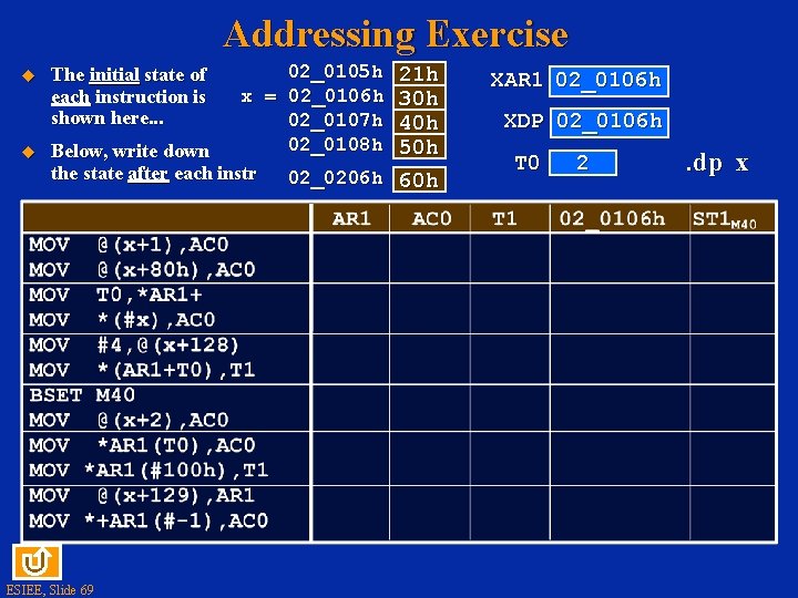
Addressing Exercise 02_0105 h x = 02_0106 h 02_0107 h 02_0108 h Below, write down the state after each instr 02_0206 h The initial state of each instruction is shown here. . . ESIEE, Slide 69 21 h 30 h 40 h 50 h 60 h XAR 1 02_0106 h XDP 02_0106 h T 0 2 . dp x

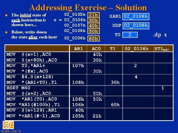
Addressing Exercise – Solution 02_0105 h x = 02_0106 h 02_0107 h 02_0108 h Below, write down the state after each instr 02_0206 h The initial state of each instruction is shown here. . . ESIEE, Slide 70 21 h 30 h 40 h 50 h 60 h XAR 1 02_0106 h XDP 02_0106 h T 0 2 . dp x

ESIEE, Slide 71

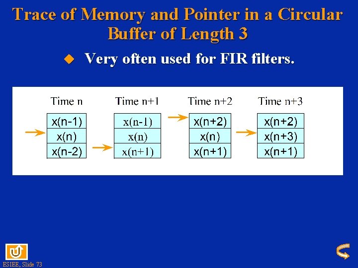
Circular buffer and circular addressing A circular buffer of length N is a block of contiguous memory words addressed by a pointer using a modulo N addressing mode. w Characteristics of a circular buffer: w w ESIEE, Slide 72 The 2 extreme words of the memory block are considered as contiguous. Instead of moving the N data in memory, just modify the pointers. When a new data x(n) arrives, the pointer is incremented and the new data is written in place of the oldest one.

Trace of Memory and Pointer in a Circular Buffer of Length 3 ESIEE, Slide 73 Very often used for FIR filters.