Driver Gate Resistor Information IGBT Gate Driver Calculation
Driver Gate Resistor Information IGBT Gate Driver Calculation Norbert Pluschke 30. 11. 2004 1
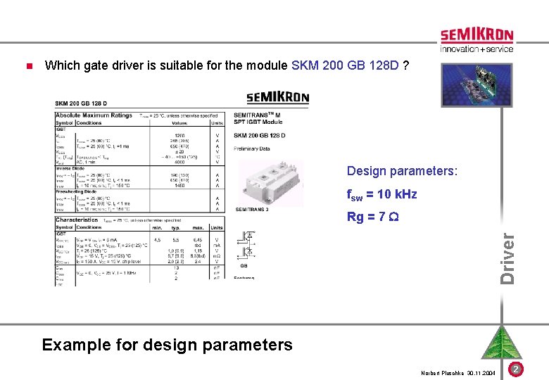
Which gate driver is suitable for the module SKM 200 GB 128 D ? Design parameters: fsw = 10 k. Hz Rg = 7 Driver n Example for design parameters Norbert Pluschke 30. 11. 2004 2
n The suitable gate driver must provide the required è Gate charge (QG) è Average current (Iout. AV) è Gate pulse current (Ig. pulse) Driver n at the applied switching frequency (fsw) Demands for the gate driver Norbert Pluschke 30. 11. 2004 3
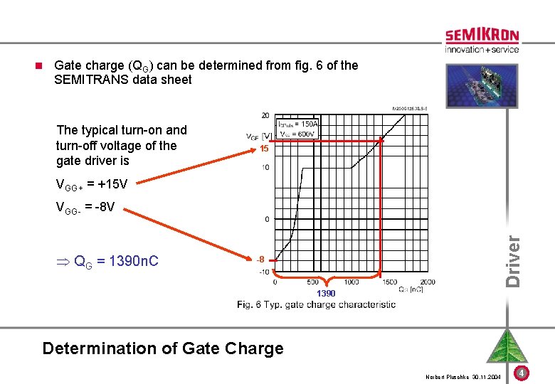
n Gate charge (QG) can be determined from fig. 6 of the SEMITRANS data sheet The typical turn-on and turn-off voltage of the gate driver is 15 VGG+ = +15 V QG = 1390 n. C Driver VGG- = -8 V -8 1390 Determination of Gate Charge Norbert Pluschke 30. 11. 2004 4
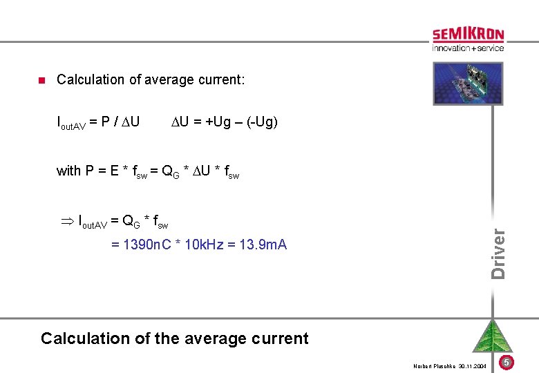
n Calculation of average current: n Iout. AV = P / U n with P = E * fsw = QG * U * fsw Iout. AV = QG * fsw Driver n U = +Ug – (-Ug) = 1390 n. C * 10 k. Hz = 13. 9 m. A Calculation of the average current Norbert Pluschke 30. 11. 2004 5
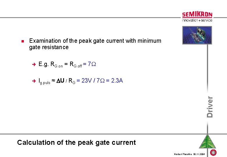
n Examination of the peak gate current with minimum gate resistance è E. g. RG. on = RG. off = 7 ≈ U / RG = 23 V / 7 = 2. 3 A Driver è Ig. puls Calculation of the peak gate current Norbert Pluschke 30. 11. 2004 6
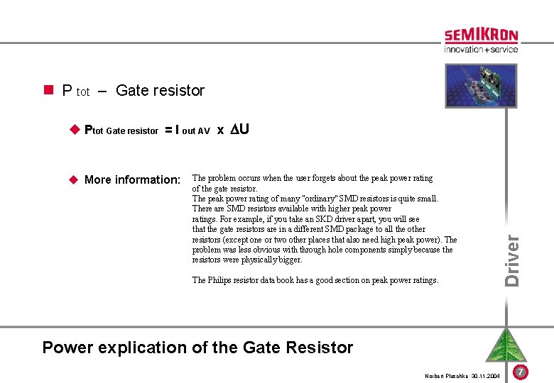
n P tot – Gate resistor u More information: The problem occurs when the user forgets about the peak power rating of the gate resistor. The peak power rating of many "ordinary" SMD resistors is quite small. There are SMD resistors available with higher peak power ratings. For example, if you take an SKD driver apart, you will see that the gate resistors are in a different SMD package to all the other resistors (except one or two other places that also need high peak power). The problem was less obvious with through hole components simply because the resistors were physically bigger. The Philips resistor data book has a good section on peak power ratings. Driver u Ptot Gate resistor = I out AV x U Power explication of the Gate Resistor Norbert Pluschke 30. 11. 2004 7
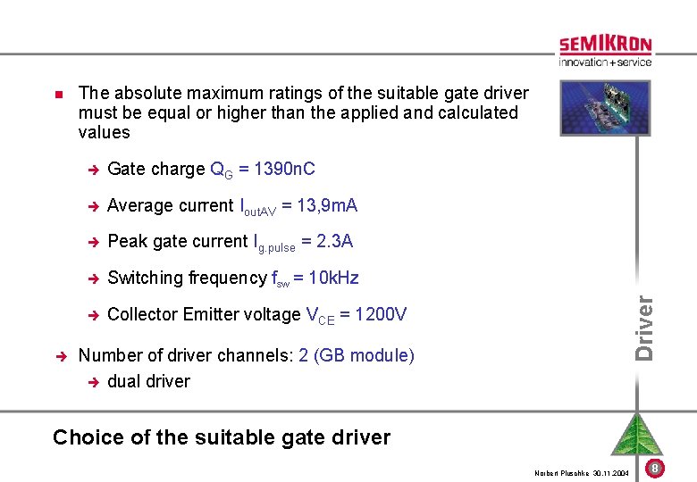
è The absolute maximum ratings of the suitable gate driver must be equal or higher than the applied and calculated values è Gate charge QG = 1390 n. C è Average current Iout. AV = 13, 9 m. A è Peak gate current Ig. pulse = 2. 3 A è Switching frequency fsw = 10 k. Hz è Collector Emitter voltage VCE = 1200 V Driver n Number of driver channels: 2 (GB module) è dual driver Choice of the suitable gate driver Norbert Pluschke 30. 11. 2004 8
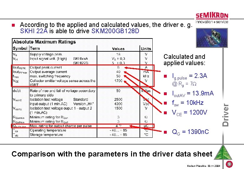
n According to the applied and calculated values, the driver e. g. SKHI 22 A is able to drive SKM 200 GB 128 D Calculated and applied values: n Ig. pulse = 2. 3 A n Iout. AV = 13. 9 m. A n fsw = 10 k. Hz n VCE = 1200 V n QG = 1390 n. C Driver @ Rg = 7 Comparison with the parameters in the driver data sheet Norbert Pluschke 30. 11. 2004 9
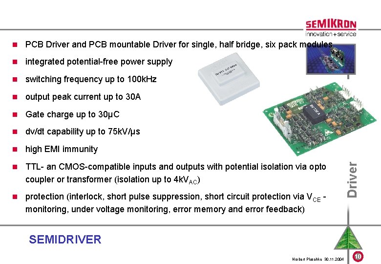
PCB Driver and PCB mountable Driver for single, half bridge, six pack modules n integrated potential-free power supply n switching frequency up to 100 k. Hz n output peak current up to 30 A n Gate charge up to 30µC n dv/dt capability up to 75 k. V/µs n high EMI immunity n TTL- an CMOS-compatible inputs and outputs with potential isolation via opto coupler or transformer (isolation up to 4 k. VAC) n protection (interlock, short pulse suppression, short circuit protection via VCE monitoring, under voltage monitoring, error memory and error feedback) Driver n SEMIDRIVER Norbert Pluschke 30. 11. 2004 10
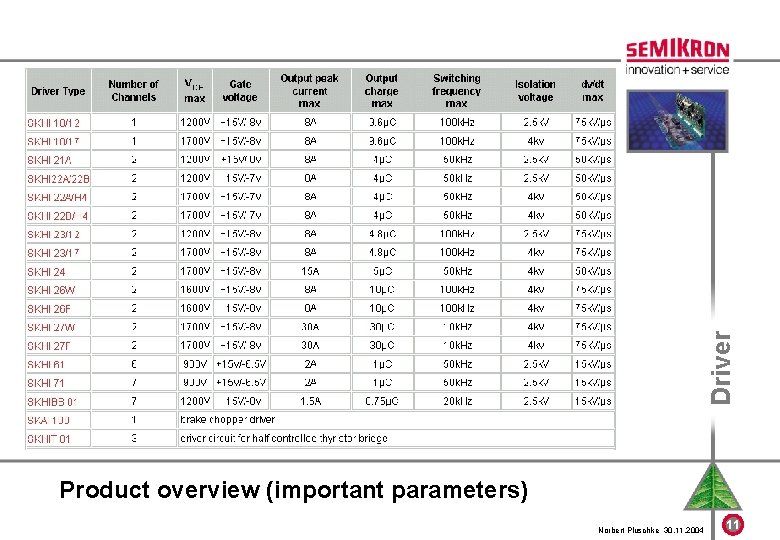
Driver Product overview (important parameters) Norbert Pluschke 30. 11. 2004 11
Driver n Many thanks for your attention. Norbert Pluschke 30. 11. 2004 12
- Slides: 12